|
|
|
- Doreen Holland
- 5 years ago
- Views:
Transcription
1
2 vidyarthiplus.com
3 vidyarthiplus.com
4 vidyarthiplus.com
5 ANNA UNIVERSITY- COMBATORE B.E./ B.TECH. DEGREE EXAMINATION - JUNE ELECTRICAL & ELECTONICS ENGG. - FOURTH SEMESTER DIGITAL LOGIC CIRCUITS PART-A Answer all questions. (20*2=40) 1. State De-Morgans theorem. 2. Briefly explain the streamlined method of converting binary to decimal number with example. 3. Give the Gray code for the binary number (111)2. 4. Subtract the following: Draw a 1 to 16 demultiplexer circuit. 6. What is priority encoder. 7. Show the common-cathode type of seven segment indicator. 8. Design a half adder using NAND gates only. 9. Draw the truth table for a NOR gate RS flip flop. 10. Obtain D flip flop from JK flip flop. 11. Differentiate synchronous counter and Asynchronous counter. 12. Draw a modulo 6 counter.hat is saturation delay time? Explain. 13. Compare bipolar family transistors with MOS family transistors. 14. what is race condition? How can it be eliminated? 15. What is essential hazard? Give an example. 16. Compare volatile data storage with non volatile data storage. 17. How is combinational logic generated in FPGA. 18. What is a DRAM? How is it refreshed? 19. Draw a macrocell of PLD.
6 PART-B Answer any five. (5*12=60) 1. Simplify the following Boolean expression using three variable maps: a) XY+X'Y'Z'+X'YZ' b) X'Y'+YZ+X'YZ' c) X'Y+YZ+Y'Z 2. Design a 3-bit parity generator circuit and the circuit of a 4-bit parity checker using even and odd parity bit. 3. Discuss in detail about state reduction problem and state assignment problem. 4. Explain the operation of clocked masterslave JK flipflop and D flipflop with neat digrams. 5. Discuss in brief about the design procedure of an asychronous circuits starting from the statement of the problem and culminates in a logic diagram. 6. Explain with a suitable example the procedure for analyzing a synchronous sequential circuit with SR latches. 7. Write short notes on : a) PAL b) FPGA 8. Discuss in detail about the types of Read only memories.
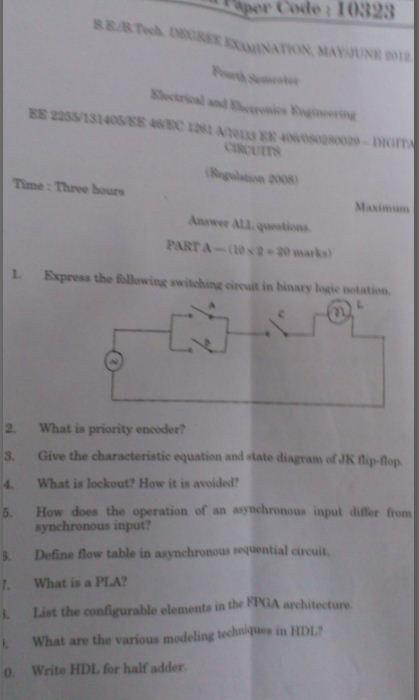
7 Reg. No. : Time: Three hours 1. Show that (a) (b) B.E./B.Tech. DEGREE EXAMINATION, APRIL/MAY 2010 a + ab ' = a+ b Fourth Semester Electrical and Electronics Engineering EE2255 DIGITAL LOGIC CIRCUITS x ' y' z+ x' yz+ xy' = x' z+ xy'. (Regulation 2008) Answer ALL Questions PART A (10 2 = 20 Marks) 2. Draw the Truth table and logic circuit of half adder. 3. Draw the circuit of SR Flip flop. 4. What are synchronous sequential circuits? 5. Give the characteristic equation and state diagram of JK flip flop. 6. What is a self starting counter? 7. What is the advantage of PLA over ROM? Maximum: 100 Marks 8. Which IC family offers (a) low propagation delay, and (b) low power dissipation? 9. Write HDL for half adder. Question Paper Code: E What are the various modeling techniques in HDL?
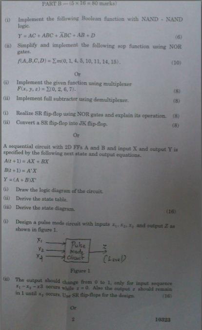
8 PART B (5 16 = 80 Marks) 11. (a) (i) Simplify using k-map F ( w, x, y, z) = (0,1,2,4,5,6,8,9,12,13,14). (8) (ii) Design a BCD to Excess-3 code converter. (8) (b) (i) Solve g ( w, x, y, z) = m(1,3,4,6,11) + d(0,8,10,12,13). (8) (ii) Design a decimal adder to add two decimal digits. (8) 12. (a) Design a synchronous sequential circuit using JK for the given state diagram. (16) (b) Design a BCD counter using T flip flop. (16) 13. (a) Design BCD ripple counter using JK flip flop. (16) (b) (i) Reduce the number of states in the following state table. (12) Next state Output Present state x = 0 x = 1 x = 0 x = 1 (ii) a f b 0 0 b d c 0 0 c f e 0 0 d g a 1 0 e d c 0 0 f f b 1 1 g g h 0 1 h g a 1 0 Starting from a, find the output sequence generated with input sequence (4) 2 E 3090
9 14. (a) (i) Design a combinatorial circuit using ROM. The circuit accepts 3-bit number and generates an output binary number equal to square of input number. (8) (ii) Repeat the above problem using PLA. (8) (b) (i) Compare all the IC logic families based on (1) Power consumption (2) Fan out (3) Power dissipation (4) Propagation delay (5) Switching speed (6) Noise margin. (8) (ii) Describe the different types of memories. (8) (b) (i) Write an HDL behavioral description of JK flip flop using if-else statement based on the value of present state. (8) (ii) Draw the logic diagram for the following module. (8) module seqcrt (A, B, C, Q, CLK) ; input A, B, C, CLK ; output Q ; reg Q, E ; (Posedge CLK) begin E < = A & B ; Q < = E/C ; end end module 3 E 3090
10 Reg. No. : Time : Three hours B.E./B.Tech. DEGREE EXAMINATION, APRIL/MAY State DeMorgan's theorem. 2. Why is MUX called as data selector? Fourth Semester Electrical and Electronics Engineering EE 2255 DIGITAL LOGIC CIRCUITS (Regulation 2008) Answer ALL questions PART A (10 2 = 20 marks) 3. Write the excitation table for JK flip flop. 4. Write the characteristics table for SR flip flop. 5. State the hazards in asynchronous sequential circuits. Maximum : 100 marks 6. What is the difference between asynchronous and synchronous sequential circuits? Question Paper Code : Name the types of ROM. 8. Define fan in and fan out characteristics of digital logic families. 9. What are ASM? 10. When can RTL be used to represent digital systems?
11 PART B (5 16 = 80 marks) 11. (a) (i) Reduce the given expressions using Boolean algebra : (1) x y z + x y z+ x yz+ xy z+ xyz (2) ab c + ab c+ a bc+ abc (3) p q' r+ p qr + p qr+ pqr + pq r. (12) (ii) For the given circuit, derive an algebraic expression in SOP form : (4) (b) (i) Reduce the following expression using k-map. (6) (ii) f = x y z+ w xz+ wxyz + wxz+ w xyz. Implement a full adder circuit with (1) Decoder (2) Multiplexer. (10) 12. (a) Draw the state diagram. Derive the state equation and draw the clocked sequential circuit for the following state table. (16) Next state Output Present state x = 0 x = 1 x = 0 x = 1 AB AB AB Y Y (b) Design BCD counter using T flip flops, where flip flop inputs are TQ 1, TQ2, TQ4 and TQ 8. (16)
12 13. (a) Design an asynchronous BCD counter. (16) (b) Describe the steps involved in design of asynchronous sequential circuit in detail with an example. (16) 14. (a) (i) Implement the following two Boolean functions with a PLA : F ( A, B, C) = (01,,2,4) 1 F ( A, B, C) = (0,5,6,7). 2 (10) (ii) Describe the characteristics of all types of memories. (6) (b) (i) Write notes on digital logic families. (9) (ii) Design ROM for the following functions. F = 1,2,3); F = (0,2). (7) 1 ( (a) Write the VHDL code for mod 6 counter. (16) (b) Describe the RTL in VHDL. (16)
13 B.E./B.Tech. DEGREE EXAMINATION, NOVEMBER/DECEMBER 2010 Fourth Semester PART A (10 2 = 20 Marks) Electrical and Electronics Engineering EE 2255 DIGITAL LOGIC CIRCUITS (Regulation 2008) Time : Three hours Maximum : 100 Marks Answer ALL questions 1. Show that Excess-3 code is self complementing. 2. Add the hexadecimal numbers: 93 and DE. 3. Convert JK flip-flop to T-flip-flop. 4. Mention the major application of Master Slave FF. 5. Draw the state diagram of SR Flip Flop. 6. Define asynchronous sequential machine. 7. State the important characteristics of TTL family. 8. In which type of TTL gate wired ANS logic is possible? 9. Write the VHDL code for AND gate. 10. List the operators available in VHDL. PART B (5 16 = 80 Marks) 11. (a) Reduce the following using tabulation method and verify with K maps. ( ) ( ) = 14, 12, 10, 8, 6, 4, 3, 2, 1, 0,,, D C B A F
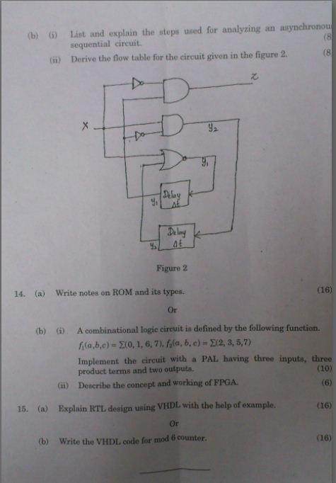
14 (b) Obtain the minimum SOP using Quine Mcclusky s method and verify using K map for the following. m13 m12 m11 m10 m9 m8 m4 m2 m0 12. (a) Design a counter with the sequence 0, 1, 3, 7, 6, 4, 0. (b) The following sequence is to be realized by a counter consisting of 3 JKFF s. A A A Design the counter. 13. (a) (i) List and explain the steps used for analyzing an asynchronous sequential circuit. (8) (ii) Describe procedure to get state table from excitation table in an asynchronous sequential circuit. How does it differ from synchronous sequential circuit? (8) (b) (i) How do you get output specifications from a flow table in asynchronous sequential circuit operating in fundamental mode? (6) (ii) When do you get the critical and non-critical races? How will you obtain race free conditions? (10) 14. (a) (i) Explain the concept, working and characteristics of TTL logic families. (8) (ii) What do you understand by FPGA? Explain the operation and applications? (8) (b) (i) Describe the working of EPROM. List the applications of EPROM.
15 (8) (ii) Discuss on the concept, operation and characteristics of CMOS technology. (8) 15. (a) Construct a VHDL module listing for a 16:1 MUX that is based on the assign statement. Use a 4-bit select word S3 S2 S1 S0 to map the selected input Pi (i = 0,...15) to the output. (b) (i) Explain the design procedure of RTL using VHDL. (10) (ii) Write a note on VHDL test benches. (6)
16 Reg. No. : B.E./B.Tech. DEGREE EXAMINATION, NOVEMBER/DECEMBER Time : Three hours Fourth Semester Electrical and Electronics Engineering EE 2255 DIGITAL LOGIC CIRCUITS (Regulation 2008) Answer ALL questions. PART A (10 2 = 20 marks) Maximum : 100 marks 1. How does don t care condition in k -map help for circuit simplification? 2. What is the difference between decoder and demultiplexer? 3. What is race around condition in Flipflops? 4. How does the state transition diagram of a Moore model differ from Mealy model? 5. What are hazards in asynchronous sequential circuits? 6. What is fundamental mode of operation in asynchronous sequential circuits? 7. What is FPGA? Question Paper Code : Why should we take care while using CMOS devices? 9. What are the operators present in VHDL? 10. What is the meaning of the following RTL Statement? T 1 : ACC ACC and MDR.
17 PART B (5 16 = 80 marks) 11. (a) Give the simplified expression for the following logic equation where d represents don t care condition. ( A, B, C, D) = Σm( 0, 8,11,12,15) d( 1, 2, 4,7,10,14) f + Represent the simplified expression using logic gates. (16) (b) Write brief notes on the following : (i) DeMorgan s theorem (4) (ii) Comparators (4) (iii) Binary to gray code converter (4) (iv) Multiplexer. (4) 12. (a) Draw the state transition diagram of a sequence detector circuit that detects 1010 from input data stream using Moore model Mealy model. (16) (b) Design a counter using JK flipflop for realizing the following sequence. (16) Q 2 Q 1 Q (a) (i) When does oscillation occur in an asynchronous sequential logic circuit? (4) (ii) Draw and explain the state transition diagram of modulo-6 counter in asynchronous sequential logic. (12)
18 (b) (i) State the condition of stability in asynchronous sequential logic. (4) (ii) Design an asynchronous sequential logic circuit for the state transition diagram shown in Fig. 13(b)(ii). (12) Fig. 13(b)(ii) 14. (a) (i) Draw and explain the NOR gate using TTL logic. (8) (ii) Write briefly about the programmable logic array and EPROM. (8) (b) (i) Discuss about the programmable logic devices. (10) (ii) Explain the characteristics of CMOS. (6) 15. (a) Explain in detail the design procedure for register transfer language. (16) (b) (i) Construct a VHDL module for a JK flipflop. (8) (ii) Express how arithmetic and logic operations are expressed using RTL. (8)
Reg. No. Question Paper Code : B.E./B.Tech. DEGREE EXAMINATION, NOVEMBER/DECEMBER Second Semester. Computer Science and Engineering
 Sp 6 Reg. No. Question Paper Code : 27156 B.E./B.Tech. DEGREE EXAMINATION, NOVEMBER/DECEMBER 2015. Second Semester Computer Science and Engineering CS 6201 DIGITAL PRINCIPLES AND SYSTEM DESIGN (Common
ELECTRONICS & COMMUNICATION ENGINEERING PROFESSIONAL ETHICS AND HUMAN VALUES
 EC 216(R-15) Total No. of Questions :09] [Total No. of Pages : 02 II/IV B.Tech. DEGREE EXAMINATIONS, DECEMBER- 2016 First Semester ELECTRONICS & COMMUNICATION ENGINEERING PROFESSIONAL ETHICS AND HUMAN
Sample Test Paper - I
 Scheme G Sample Test Paper - I Course Name : Computer Engineering Group Marks : 25 Hours: 1 Hrs. Q.1) Attempt any THREE: 09 Marks a) Define i) Propagation delay ii) Fan-in iii) Fan-out b) Convert the following:
KUMARAGURU COLLEGE OF TECHNOLOGY COIMBATORE
 Estd-1984 KUMARAGURU COLLEGE OF TECHNOLOGY COIMBATORE 641 006 QUESTION BANK UNIT I PART A ISO 9001:2000 Certified 1. Convert (100001110.010) 2 to a decimal number. 2. Find the canonical SOP for the function
Show that the dual of the exclusive-or is equal to its compliment. 7
 Darshan Institute of ngineering and Technology, Rajkot, Subject: Digital lectronics (2300) GTU Question ank Unit Group Questions Do as directed : I. Given that (6)0 = (00)x, find the value of x. II. dd
LOGIC CIRCUITS. Basic Experiment and Design of Electronics. Ho Kyung Kim, Ph.D.
 Basic Experiment and Design of Electronics LOGIC CIRCUITS Ho Kyung Kim, Ph.D. hokyung@pusan.ac.kr School of Mechanical Engineering Pusan National University Digital IC packages TTL (transistor-transistor
DHANALAKSHMI COLLEGE OF ENGINEERING, CHENNAI DEPARTMENT OF COMPUTER SCIENCE AND ENGINEERING CS6201 DIGITAL PRINCIPLES AND SYSTEM DESIGN
 DHANALAKSHMI COLLEGE OF ENGINEERING, CHENNAI DEPARTMENT OF COMPUTER SCIENCE AND ENGINEERING CS6201 DIGITAL PRINCIPLES AND SYSTEM DESIGN UNIT I : BOOLEAN ALGEBRA AND LOGIC GATES PART - A (2 MARKS) Number
LOGIC CIRCUITS. Basic Experiment and Design of Electronics
 Basic Experiment and Design of Electronics LOGIC CIRCUITS Ho Kyung Kim, Ph.D. hokyung@pusan.ac.kr School of Mechanical Engineering Pusan National University Outline Combinational logic circuits Output
( c) Give logic symbol, Truth table and circuit diagram for a clocked SR flip-flop. A combinational circuit is defined by the function
 Give logic symbol, Truth table and circuit diagram for a clocked SR flip-flop. A combinational circuit is defined by the function") Question Paper Digital Electronics (EE-204-F) MDU Examination May 2015 1. (a) represent (32)10 in (i) BCD 8421 code (ii) Excess-3 code (iii) ASCII code (b) Design half adder using only NAND gates. ( c)
Question Paper Digital Electronics (EE-204-F) MDU Examination May 2015 1. (a) represent (32)10 in (i) BCD 8421 code (ii) Excess-3 code (iii) ASCII code (b) Design half adder using only NAND gates. ( c)
SIR C.R.REDDY COLLEGE OF ENGINEERING ELURU DIGITAL INTEGRATED CIRCUITS (DIC) LABORATORY MANUAL III / IV B.E. (ECE) : I - SEMESTER
 LABORATORY MANUAL III / IV B.E. (ECE) : I - SEMESTER") SIR C.R.REDDY COLLEGE OF ENGINEERING ELURU 534 007 DIGITAL INTEGRATED CIRCUITS (DIC) LABORATORY MANUAL III / IV B.E. (ECE) : I - SEMESTER DEPARTMENT OF ELECTRONICS AND COMMUNICATION ENGINEERING DIGITAL
SIR C.R.REDDY COLLEGE OF ENGINEERING ELURU 534 007 DIGITAL INTEGRATED CIRCUITS (DIC) LABORATORY MANUAL III / IV B.E. (ECE) : I - SEMESTER DEPARTMENT OF ELECTRONICS AND COMMUNICATION ENGINEERING DIGITAL
MODEL ANSWER SUMMER 17 EXAMINATION Subject Title: Principles of Digital Techniques
 MODEL ANSWER SUMMER 17 EXAMINATION Subject Title: Principles of Digital Techniques Subject Code: Important Instructions to examiners: 1) The answers should be examined by key words and not as word-to-word
Department of Electrical & Electronics EE-333 DIGITAL SYSTEMS
 Department of Electrical & Electronics EE-333 DIGITAL SYSTEMS 1) Given the two binary numbers X = 1010100 and Y = 1000011, perform the subtraction (a) X -Y and (b) Y - X using 2's complements. a) X = 1010100
Appendix B. Review of Digital Logic. Baback Izadi Division of Engineering Programs
 Appendix B Review of Digital Logic Baback Izadi Division of Engineering Programs bai@engr.newpaltz.edu Elect. & Comp. Eng. 2 DeMorgan Symbols NAND (A.B) = A +B NOR (A+B) = A.B AND A.B = A.B = (A +B ) OR
Vidyalankar S.E. Sem. III [CMPN] Digital Logic Design and Analysis Prelim Question Paper Solution
![Vidyalankar S.E. Sem. III [CMPN] Digital Logic Design and Analysis Prelim Question Paper Solution](/thumbs/90/103673562.jpg "Vidyalankar S.E. Sem. III [CMPN] Digital Logic Design and Analysis Prelim Question Paper Solution") . (a) (i) ( B C 5) H (A 2 B D) H S.E. Sem. III [CMPN] Digital Logic Design and Analysis Prelim Question Paper Solution ( B C 5) H (A 2 B D) H = (FFFF 698) H (ii) (2.3) 4 + (22.3) 4 2 2. 3 2. 3 2 3. 2 (2.3)
. (a) (i) ( B C 5) H (A 2 B D) H S.E. Sem. III [CMPN] Digital Logic Design and Analysis Prelim Question Paper Solution ( B C 5) H (A 2 B D) H = (FFFF 698) H (ii) (2.3) 4 + (22.3) 4 2 2. 3 2. 3 2 3. 2 (2.3)
S.Y. Diploma : Sem. III [DE/ED/EI/EJ/EN/ET/EV/EX/IC/IE/IS/IU/MU] Principles of Digital Techniques
![S.Y. Diploma : Sem. III [DE/ED/EI/EJ/EN/ET/EV/EX/IC/IE/IS/IU/MU] Principles of Digital Techniques](/thumbs/82/86792063.jpg "S.Y. Diploma : Sem. III [DE/ED/EI/EJ/EN/ET/EV/EX/IC/IE/IS/IU/MU] Principles of Digital Techniques") S.Y. Diploma : Sem. III [DE/ED/EI/EJ/EN/ET/EV/EX/IC/IE/IS/IU/MU] Principles of Digital Techniques Time: 3 Hrs.] Prelim Question Paper Solution [Marks : 100 Q.1(a) Attempt any SIX of the following : [12]
S.Y. Diploma : Sem. III [DE/ED/EI/EJ/EN/ET/EV/EX/IC/IE/IS/IU/MU] Principles of Digital Techniques Time: 3 Hrs.] Prelim Question Paper Solution [Marks : 100 Q.1(a) Attempt any SIX of the following : [12]
Fundamentals of Digital Design
 Fundamentals of Digital Design Digital Radiation Measurement and Spectroscopy NE/RHP 537 1 Binary Number System The binary numeral system, or base-2 number system, is a numeral system that represents numeric
MAHARASHTRA STATE BOARD OF TECHNICAL EDUCATION (Autonomous) (ISO/IEC Certified)
 (ISO/IEC Certified)") WINTER 17 EXAMINATION Subject Name: Digital Techniques Model Answer Subject Code: 17333 Important Instructions to examiners: 1) The answers should be examined by key words and not as word-to-word as given
WINTER 17 EXAMINATION Subject Name: Digital Techniques Model Answer Subject Code: 17333 Important Instructions to examiners: 1) The answers should be examined by key words and not as word-to-word as given
on candidate s understanding. 7) For programming language papers, credit may be given to any other program based on equivalent concept.
 For programming language papers, credit may be given to any other program based on equivalent concept.") WINTER 17 EXAMINATION Subject Name: Digital Techniques Model Answer Subject Code: 17333 Important Instructions to examiners: 1) The answers should be examined by key words and not as word-to-word as given
WINTER 17 EXAMINATION Subject Name: Digital Techniques Model Answer Subject Code: 17333 Important Instructions to examiners: 1) The answers should be examined by key words and not as word-to-word as given
DIGITAL LOGIC CIRCUITS
 DIGITAL LOGIC CIRCUITS Introduction Logic Gates Boolean Algebra Map Specification Combinational Circuits Flip-Flops Sequential Circuits Memory Components Integrated Circuits Digital Computers 2 LOGIC GATES
A B D 1 Y D 2 D 3. Truth table for 4 to 1 MUX: A B Y 0 0 D D D D 3
 . What is a multiplexer? esign a 4 to multiplexer using logic gates. Write the truth table and explain its working principle. Answer: is a circuit with many inputs but only one output. esigning of 4 to
S.Y. Diploma : Sem. III [CO/CM/IF/CD/CW] Digital Techniques
![S.Y. Diploma : Sem. III [CO/CM/IF/CD/CW] Digital Techniques](/thumbs/90/103932933.jpg "S.Y. Diploma : Sem. III [CO/CM/IF/CD/CW] Digital Techniques") S.Y. Diploma : Sem. III [CO/CM/IF/CD/CW] Digital Techniques Time: 3 Hrs.] Prelim Question Paper Solution [Marks : 100 Q.1(a) Attempt any SIX of the following : [12] Q.1(a) (i) Derive AND gate and OR gate
S.Y. Diploma : Sem. III [CO/CM/IF/CD/CW] Digital Techniques Time: 3 Hrs.] Prelim Question Paper Solution [Marks : 100 Q.1(a) Attempt any SIX of the following : [12] Q.1(a) (i) Derive AND gate and OR gate
3 Logic Function Realization with MSI Circuits
 3 Logic Function Realization with MSI Circuits Half adder A half-adder is a combinational circuit with two binary inputs (augund and addend bits) and two binary outputs (sum and carry bits). It adds the
SAU1A FUNDAMENTALS OF DIGITAL COMPUTERS
 SAU1A FUNDAMENTALS OF DIGITAL COMPUTERS Unit : I - V Unit : I Overview Fundamentals of Computers Characteristics of Computers Computer Language Operating Systems Generation of Computers 2 Definition of
INSTITUTEOFAERONAUTICALENGINEERING (Autonomous) Dundigal, Hyderabad
 Dundigal, Hyderabad") INSTITUTEOFAERONAUTICALENGINEERING (Autonomous) Dundigal, Hyderabad - 50004 COMPUTER SCIENCE AND ENGINEERING TUTORIAL QUESTION BANK Course Name Course Code Class Branch DIGITAL LOGIC DESIGN A040 II B.
INSTITUTEOFAERONAUTICALENGINEERING (Autonomous) Dundigal, Hyderabad - 50004 COMPUTER SCIENCE AND ENGINEERING TUTORIAL QUESTION BANK Course Name Course Code Class Branch DIGITAL LOGIC DESIGN A040 II B.
MAHARASHTRA STATE BOARD OF TECHNICAL EDUCATION
 MAHARASHTRA STATE BOARD OF TECHNICAL EDUCATION (Autonomous) (ISO/IEC - 27001-2005 Certified) Subject Code: 12069 SUMMER 13 EXAMINATION Model Answer Important Instructions to examiners: 1) The answers should
MAHALAKSHMI ENGINEERING COLLEGE TIRUCHIRAPALLI
 MAHALAKSHMI ENGINEERING COLLEGE TIRUCHIRAPALLI 6 DEPARTMENT: EEE QUESTION BANK SUBJECT NAME: DIGITAL LOGIC CIRCUITS SUBJECT CODE: EE55 SEMESTER IV UNIT : Design of Synchronous Sequential Circuits PART
EE40 Lec 15. Logic Synthesis and Sequential Logic Circuits
 EE40 Lec 15 Logic Synthesis and Sequential Logic Circuits Prof. Nathan Cheung 10/20/2009 Reading: Hambley Chapters 7.4-7.6 Karnaugh Maps: Read following before reading textbook http://www.facstaff.bucknell.edu/mastascu/elessonshtml/logic/logic3.html
Dept. of ECE, CIT, Gubbi Page 1
 Verification: 1) A.B = A + B 7404 7404 7404 A B A.B A.B 0 0 0 1 0 1 0 1 1 0 0 1 1 1 1 0 A B A B A + B 0 0 1 1 1 0 1 1 0 1 1 0 0 1 1 1 1 0 0 0 2) A+B = A. B 7404 7404 7404 A B A+B A+B 0 0 0 1 0 1 1 0 1
Section 3: Combinational Logic Design. Department of Electrical Engineering, University of Waterloo. Combinational Logic
 Section 3: Combinational Logic Design Major Topics Design Procedure Multilevel circuits Design with XOR gates Adders and Subtractors Binary parallel adder Decoders Encoders Multiplexers Programmed Logic
MAHALAKSHMI ENGINEERING COLLEGE TIRUCHIRAPALLI
 DEPARTMENT: ECE MAHALAKSHMI ENGINEERING COLLEGE TIRUCHIRAPALLI 6 QUESTION BANK SUBJECT NAME: DIGITAL ELECTRONICS UNIT : Design of Sequential Circuits PART A ( Marks). Draw the logic diagram 4: Multiplexer.(AUC
Chapter 4. Combinational: Circuits with logic gates whose outputs depend on the present combination of the inputs. elements. Dr.
 Chapter 4 Dr. Panos Nasiopoulos Combinational: Circuits with logic gates whose outputs depend on the present combination of the inputs. Sequential: In addition, they include storage elements Combinational
MAHARASHTRA STATE BOARD OF TECHNICAL EDUCATION (Autonomous) (ISO/IEC Certified) State any two Boolean laws. (Any 2 laws 1 mark each)
 (ISO/IEC Certified) State any two Boolean laws. (Any 2 laws 1 mark each)") Subject Code: 17333 Model Answer Page 1/ 27 Important Instructions to examiners: 1) The answers should be examined by key words and not as word-to-word as given in the model answer scheme. 2) The model
Subject Code: 17333 Model Answer Page 1/ 27 Important Instructions to examiners: 1) The answers should be examined by key words and not as word-to-word as given in the model answer scheme. 2) The model
Fundamentals of Computer Systems
 Fundamentals of Computer Systems Review for the Final Stephen A. Edwards Columbia University Summer 25 The Final 2 hours 8 problems Closed book Simple calculators are OK, but unnecessary One double-sided
ECEN 248: INTRODUCTION TO DIGITAL SYSTEMS DESIGN. Week 9 Dr. Srinivas Shakkottai Dept. of Electrical and Computer Engineering
 ECEN 248: INTRODUCTION TO DIGITAL SYSTEMS DESIGN Week 9 Dr. Srinivas Shakkottai Dept. of Electrical and Computer Engineering TIMING ANALYSIS Overview Circuits do not respond instantaneously to input changes
ECE 545 Digital System Design with VHDL Lecture 1. Digital Logic Refresher Part A Combinational Logic Building Blocks
 ECE 545 Digital System Design with VHDL Lecture Digital Logic Refresher Part A Combinational Logic Building Blocks Lecture Roadmap Combinational Logic Basic Logic Review Basic Gates De Morgan s Law Combinational
DE58/DC58 LOGIC DESIGN DEC 2014
 Q.2 a. In a base-5 number system, 3 digit representations is used. Find out (i) Number of distinct quantities that can be represented.(ii) Representation of highest decimal number in base-5. Since, r=5
Vidyalankar S.E. Sem. III [EXTC] Digital Electronics Prelim Question Paper Solution ABCD ABCD ABCD ABCD ABCD ABCD ABCD ABCD = B
![Vidyalankar S.E. Sem. III [EXTC] Digital Electronics Prelim Question Paper Solution ABCD ABCD ABCD ABCD ABCD ABCD ABCD ABCD = B](/thumbs/84/91058397.jpg "Vidyalankar S.E. Sem. III [EXTC] Digital Electronics Prelim Question Paper Solution ABCD ABCD ABCD ABCD ABCD ABCD ABCD ABCD = B") . (a). (b). (c) S.E. Sem. III [EXTC] igital Electronics Prelim Question Paper Solution ABC ABC ABC ABC ABC ABC ABC ABC = B LHS = ABC ABC ABC ABC ABC ABC ABC ABC But ( ) = = ABC( ) ABC( ) ABC( ) ABC( )
. (a). (b). (c) S.E. Sem. III [EXTC] igital Electronics Prelim Question Paper Solution ABC ABC ABC ABC ABC ABC ABC ABC = B LHS = ABC ABC ABC ABC ABC ABC ABC ABC But ( ) = = ABC( ) ABC( ) ABC( ) ABC( )
Digital Electronics Circuits 2017
 JSS SCIENCE AND TECHNOLOGY UNIVERSITY Digital Electronics Circuits (EC37L) Lab in-charge: Dr. Shankraiah Course outcomes: After the completion of laboratory the student will be able to, 1. Simplify, design
Philadelphia University Student Name: Student Number:
 Philadelphia University Student Name: Student Number: Faculty of Engineering Serial Number: Final Exam, Second Semester: 2015/2016 Dept. of Computer Engineering Course Title: Logic Circuits Date: 08/06/2016
UNIVERSITI TENAGA NASIONAL. College of Information Technology
 UNIVERSITI TENAGA NASIONAL College of Information Technology BACHELOR OF COMPUTER SCIENCE (HONS.) FINAL EXAMINATION SEMESTER 2 2012/2013 DIGITAL SYSTEMS DESIGN (CSNB163) January 2013 Time allowed: 3 hours
Fundamentals of Computer Systems
 Fundamentals of Computer Systems Review for the Midterm Stephen A. Edwards Columbia University Spring 22 The Midterm 75 minutes 4 5 problems Closed book Simple calculators are OK, but unnecessary One double-sided
Review for B33DV2-Digital Design. Digital Design
 Review for B33DV2 The Elements of Modern Behaviours Design Representations Blocks Waveforms Gates Truth Tables Boolean Algebra Switches Rapid Prototyping Technologies Circuit Technologies TTL MOS Simulation
Combinational Logic. Mantıksal Tasarım BBM231. section instructor: Ufuk Çelikcan
 Combinational Logic Mantıksal Tasarım BBM23 section instructor: Ufuk Çelikcan Classification. Combinational no memory outputs depends on only the present inputs expressed by Boolean functions 2. Sequential
CHW 261: Logic Design
 CHW 26: Logic Design Instructors: Prof. Hala Zayed Dr. Ahmed Shalaby http://www.bu.edu.eg/staff/halazayed4 http://bu.edu.eg/staff/ahmedshalaby4# Slide Digital Fundamentals Digital Concepts Slide 2 What?
Digital Circuits and Design
 Digital Circuits and Design S. Salivahanan Principal, SSN College of Engineering Chennai S. Arivazhagan Principal, Mepco Schlenk Engineering College Sivakasi. All rights reserved. 3 is a department of
Boolean Algebra and Digital Logic 2009, University of Colombo School of Computing
 IT 204 Section 3.0 Boolean Algebra and Digital Logic Boolean Algebra 2 Logic Equations to Truth Tables X = A. B + A. B + AB A B X 0 0 0 0 3 Sum of Products The OR operation performed on the products of
Combinational Logic Design Combinational Functions and Circuits
 Combinational Logic Design Combinational Functions and Circuits Overview Combinational Circuits Design Procedure Generic Example Example with don t cares: BCD-to-SevenSegment converter Binary Decoders
WORKBOOK. Try Yourself Questions. Electrical Engineering Digital Electronics. Detailed Explanations of
 27 WORKBOOK Detailed Eplanations of Try Yourself Questions Electrical Engineering Digital Electronics Number Systems and Codes T : Solution Converting into decimal number system 2 + 3 + 5 + 8 2 + 4 8 +
DIGITAL LOGIC DESIGN
 DIGITAL LOGIC DESIGN NUMBERS SYSTEMS AND CODES Any number in one base system can be converted into another base system Types 1) decimal to any base 2) Any base to decimal 3) Any base to Any base Complements
Fundamentals of Boolean Algebra
 UNIT-II 1 Fundamentals of Boolean Algebra Basic Postulates Postulate 1 (Definition): A Boolean algebra is a closed algebraic system containing a set K of two or more elements and the two operators and
CPE/EE 422/522. Chapter 1 - Review of Logic Design Fundamentals. Dr. Rhonda Kay Gaede UAH. 1.1 Combinational Logic
 CPE/EE 422/522 Chapter - Review of Logic Design Fundamentals Dr. Rhonda Kay Gaede UAH UAH Chapter CPE/EE 422/522. Combinational Logic Combinational Logic has no control inputs. When the inputs to a combinational
Review for Test 1 : Ch1 5
 Review for Test 1 : Ch1 5 October 5, 2006 Typeset by FoilTEX Positional Numbers 527.46 10 = (5 10 2 )+(2 10 1 )+(7 10 0 )+(4 10 1 )+(6 10 2 ) 527.46 8 = (5 8 2 ) + (2 8 1 ) + (7 8 0 ) + (4 8 1 ) + (6 8
Logic. Combinational. inputs. outputs. the result. system can
 Digital Electronics Combinational Logic Functions Digital logic circuits can be classified as either combinational or sequential circuits. A combinational circuit is one where the output at any time depends
Philadelphia University Student Name: Student Number:
 Philadelphia University Student Name: Student Number: Faculty of Engineering Serial Number: Final Exam, First Semester: 2017/2018 Dept. of Computer Engineering Course Title: Logic Circuits Date: 29/01/2018
Written exam for IE1204/5 Digital Design with solutions Thursday 29/
 Written exam for IE4/5 Digital Design with solutions Thursday 9/ 5 9.-. General Information Examiner: Ingo Sander. Teacher: William Sandqvist phone 8-794487 Exam text does not have to be returned when
Synchronous Sequential Logic
 1 IT 201 DIGITAL SYSTEMS DESIGN MODULE4 NOTES Synchronous Sequential Logic Sequential Circuits - A sequential circuit consists of a combinational circuit and a feedback through the storage elements in
Chapter 7 Logic Circuits
 Chapter 7 Logic Circuits Goal. Advantages of digital technology compared to analog technology. 2. Terminology of Digital Circuits. 3. Convert Numbers between Decimal, Binary and Other forms. 5. Binary
Digital Logic: Boolean Algebra and Gates. Textbook Chapter 3
 Digital Logic: Boolean Algebra and Gates Textbook Chapter 3 Basic Logic Gates XOR CMPE12 Summer 2009 02-2 Truth Table The most basic representation of a logic function Lists the output for all possible
Digital Logic Appendix A
 Digital Logic Appendix A Boolean Algebra Gates Combinatorial Circuits Sequential Circuits 1 Boolean Algebra George Boole ideas 1854 Claude Shannon, apply to circuit design, 1938 Describe digital circuitry
Lecture 7: Logic design. Combinational logic circuits
 /24/28 Lecture 7: Logic design Binary digital circuits: Two voltage levels: and (ground and supply voltage) Built from transistors used as on/off switches Analog circuits not very suitable for generic
S.E. Sem. III [ETRX] Digital Circuit Design. t phl. Fig.: Input and output voltage waveforms to define propagation delay times.
![S.E. Sem. III [ETRX] Digital Circuit Design. t phl. Fig.: Input and output voltage waveforms to define propagation delay times.](/thumbs/93/111090909.jpg "S.E. Sem. III [ETRX] Digital Circuit Design. t phl. Fig.: Input and output voltage waveforms to define propagation delay times.") S.E. Sem. III [ETRX] Digital ircuit Design Time : 3 Hrs.] Prelim Paper Solution [Marks : 80. Solve following : [20].(a) Explain characteristics of logic families. [5] haracteristics of logic families are
S.E. Sem. III [ETRX] Digital ircuit Design Time : 3 Hrs.] Prelim Paper Solution [Marks : 80. Solve following : [20].(a) Explain characteristics of logic families. [5] haracteristics of logic families are
CSE140: Components and Design Techniques for Digital Systems. Midterm Information. Instructor: Mohsen Imani. Sources: TSR, Katz, Boriello & Vahid
 CSE140: Components and Design Techniques for Digital Systems Midterm Information Instructor: Mohsen Imani Midterm Topics In general: everything that was covered in homework 1 and 2 and related lectures,
Contents. Chapter 3 Combinational Circuits Page 1 of 36
 Chapter 3 Combinational Circuits Page of 36 Contents Combinational Circuits...2 3. Analysis of Combinational Circuits...3 3.. Using a Truth Table...3 3..2 Using a Boolean Function...6 3.2 Synthesis of
Written reexam with solutions for IE1204/5 Digital Design Monday 14/
 Written reexam with solutions for IE204/5 Digital Design Monday 4/3 206 4.-8. General Information Examiner: Ingo Sander. Teacher: William Sandqvist phone 08-7904487 Exam text does not have to be returned
DIGITAL LOGIC CIRCUITS
 DIGITAL LOGIC CIRCUITS Introduction Logic Gates Boolean Algebra Map Specification Combinational Circuits Flip-Flops Sequential Circuits Memor Components Integrated Circuits BASIC LOGIC BLOCK - GATE - Logic
Vidyalankar S.E. Sem. III [ETRX] Digital Circuits and Design Prelim Question Paper Solution
![Vidyalankar S.E. Sem. III [ETRX] Digital Circuits and Design Prelim Question Paper Solution](/thumbs/79/79145081.jpg "Vidyalankar S.E. Sem. III [ETRX] Digital Circuits and Design Prelim Question Paper Solution") S.E. Sem. III [ETRX] Digital Circuits and Design Prelim uestion Paper Solution. (a) Static Hazard Static hazards have two cases: static and static. static- hazard exists when the output variable should
S.E. Sem. III [ETRX] Digital Circuits and Design Prelim uestion Paper Solution. (a) Static Hazard Static hazards have two cases: static and static. static- hazard exists when the output variable should
King Fahd University of Petroleum and Minerals College of Computer Science and Engineering Computer Engineering Department
 King Fahd University of Petroleum and Minerals College of Computer Science and Engineering Computer Engineering Department Page 1 of 13 COE 202: Digital Logic Design (3-0-3) Term 112 (Spring 2012) Final
Philadelphia University Faculty of Engineering
 Philadelphia University Faculty of Engineering Marking Scheme Exam Paper BSc CE Logic Circuits (630211) Final Exam First semester ate: 03/02/2019 Section 1 Weighting 40% of the module total Lecturer: Coordinator:
MAHARASHTRA STATE BOARD OF TECHNICAL EDUCATION (Autonomous) (ISO/IEC Certified) SUMMER 14 EXAMINATION Model Answer
 (ISO/IEC Certified) SUMMER 14 EXAMINATION Model Answer") MAHARASHTRA STATE BOARD OF TECHNICAL EDUCATION (Autonomous) (ISO/IEC 27001 2005 Certified) SUMMER 14 EXAMINATION Model Answer Subject Code : 17320 Page No: 1/34 Important Instructions to examiners: 1)
MAHARASHTRA STATE BOARD OF TECHNICAL EDUCATION (Autonomous) (ISO/IEC 27001 2005 Certified) SUMMER 14 EXAMINATION Model Answer Subject Code : 17320 Page No: 1/34 Important Instructions to examiners: 1)
ELEC Digital Logic Circuits Fall 2014 Sequential Circuits (Chapter 6) Finite State Machines (Ch. 7-10)
 Finite State Machines (Ch. 7-10)") ELEC 2200-002 Digital Logic Circuits Fall 2014 Sequential Circuits (Chapter 6) Finite State Machines (Ch. 7-10) Vishwani D. Agrawal James J. Danaher Professor Department of Electrical and Computer Engineering
ELEC 2200-002 Digital Logic Circuits Fall 2014 Sequential Circuits (Chapter 6) Finite State Machines (Ch. 7-10) Vishwani D. Agrawal James J. Danaher Professor Department of Electrical and Computer Engineering
(Boolean Algebra, combinational circuits) (Binary Codes and -arithmetics)
 (Binary Codes and -arithmetics)") Task 1. Exercises: Logical Design of Digital Systems Seite: 1 Self Study (Boolean Algebra, combinational circuits) 1.1 Minimize the function f 1 a ab ab by the help of Boolean algebra and give an implementation
Task 1. Exercises: Logical Design of Digital Systems Seite: 1 Self Study (Boolean Algebra, combinational circuits) 1.1 Minimize the function f 1 a ab ab by the help of Boolean algebra and give an implementation
Boolean Algebra. Digital Logic Appendix A. Postulates, Identities in Boolean Algebra How can I manipulate expressions?
 Digital Logic Appendix A Gates Combinatorial Circuits Sequential Circuits Other operations NAND A NAND B = NOT ( A ANDB) = AB NOR A NOR B = NOT ( A ORB) = A + B Truth tables What is the result of the operation
CHAPTER 7. Exercises 17/ / /2 2 0
 CHAPTER 7 Exercises E7. (a) For the whole part, we have: Quotient Remainders 23/2 /2 5 5/2 2 2/2 0 /2 0 Reading the remainders in reverse order, we obtain: 23 0 = 0 2 For the fractional part we have 2
Lecture A: Logic Design and Gates
 Lecture A: Logic Design and Gates Syllabus My office hours 9.15-10.35am T,Th or gchoi@ece.tamu.edu 333G WERC Text: Brown and Vranesic Fundamentals of Digital Logic,» Buy it.. Or borrow it» Other book:
EE 209 Logic Cumulative Exam Name:
 EE 209 Logic Cumulative Exam Name: 1.) Answer the following questions as True or False a.) A 4-to-1 multiplexer requires at least 4 select lines: true / false b.) An 8-to-1 mux and no other logi can be
Sequential vs. Combinational
 Sequential Circuits Sequential vs. Combinational Combinational Logic: Output depends only on current input TV channel selector (-9) inputs system outputs Sequential Logic: Output depends not only on current
Appendix A: Digital Logic. Principles of Computer Architecture. Principles of Computer Architecture by M. Murdocca and V. Heuring
 - Principles of Computer rchitecture Miles Murdocca and Vincent Heuring 999 M. Murdocca and V. Heuring -2 Chapter Contents. Introduction.2 Combinational Logic.3 Truth Tables.4 Logic Gates.5 Properties
COSC 243. Introduction to Logic And Combinatorial Logic. Lecture 4 - Introduction to Logic and Combinatorial Logic. COSC 243 (Computer Architecture)
") COSC 243 Introduction to Logic And Combinatorial Logic 1 Overview This Lecture Introduction to Digital Logic Gates Boolean algebra Combinatorial Logic Source: Chapter 11 (10 th edition) Source: J.R. Gregg,
COSC 243 Introduction to Logic And Combinatorial Logic 1 Overview This Lecture Introduction to Digital Logic Gates Boolean algebra Combinatorial Logic Source: Chapter 11 (10 th edition) Source: J.R. Gregg,
Written exam with solutions IE1204/5 Digital Design Monday 23/
 Written exam with solutions IE204/5 Digital Design Monday 23/0 207 4.00-8.00 General Information Examiner: Ingo Sander. Teacher: Kista, William Sandvist Exam text has to be returned when you hand in your
Models for representing sequential circuits
 Sequential Circuits Models for representing sequential circuits Finite-state machines (Moore and Mealy) Representation of memory (states) Changes in state (transitions) Design procedure State diagrams
Save from: cs. Logic design 1 st Class أستاذ المادة: د. عماد
 Save from: www.uotiq.org/dep cs Logic design 1 st Class أستاذ المادة: د. عماد استاذة المادة: م.م ميساء Contents Lectured One: Number system operation 1- Decimal numbers. 2- Binary numbers. 3- Octal numbers.
TYPICAL QUESTIONS & ANSWERS
 TYPICAL QUESTIONS & ANSWERS PART - I OJECTIVE TYPE QUESTIONS Each Question carries 2 marks. Choose correct or the best alternative in the following: Q.1 The NAN gate output will be low if the two inputs
Cs302 Quiz for MID TERM Exam Solved
 Question # 1 of 10 ( Start time: 01:30:33 PM ) Total Marks: 1 Caveman used a number system that has distinct shapes: 4 5 6 7 Question # 2 of 10 ( Start time: 01:31:25 PM ) Total Marks: 1 TTL based devices
Digital Logic and Design (Course Code: EE222) Lecture 1 5: Digital Electronics Fundamentals. Evolution of Electronic Devices
 Lecture 1 5: Digital Electronics Fundamentals. Evolution of Electronic Devices") Indian Institute of Technolog Jodhpur, Year 207 208 Digital Logic and Design (Course Code: EE222) Lecture 5: Digital Electronics Fundamentals Course Instructor: Shree Prakash Tiwari Email: sptiwari@iitj.ac.in
Indian Institute of Technolog Jodhpur, Year 207 208 Digital Logic and Design (Course Code: EE222) Lecture 5: Digital Electronics Fundamentals Course Instructor: Shree Prakash Tiwari Email: sptiwari@iitj.ac.in
Chapter 4: Designing Combinational Systems Uchechukwu Ofoegbu
 Chapter 4: Designing Combinational Systems Uchechukwu Ofoegbu Temple University Gate Delay ((1.1).1) ((1.0).0) ((0.1).1) ((0.1).0) ((1.1) = 1 0 s = sum c out carry-out a, b = added bits C = carry in a
FSM model for sequential circuits
 1 FSM model for sequential circuits The mathematical model of a sequential circuit is called finite-state machine. FSM is fully characterized by: S Finite set of states ( state ~ contents of FFs) I Finite
EECS Components and Design Techniques for Digital Systems. FSMs 9/11/2007
 EECS 150 - Components and Design Techniques for Digital Systems FSMs 9/11/2007 Sarah Bird Electrical Engineering and Computer Sciences University of California, Berkeley Slides borrowed from David Culler
Boolean Algebra. Digital Logic Appendix A. Boolean Algebra Other operations. Boolean Algebra. Postulates, Identities in Boolean Algebra
 Digital Logic Appendix A Gates Combinatorial Circuits Sequential Circuits George Boole ideas 1854 Claude Shannon, apply to circuit design, 1938 (piirisuunnittelu) Describe digital circuitry function programming
Systems I: Computer Organization and Architecture
 Systems I: Computer Organization and Architecture Lecture 6 - Combinational Logic Introduction A combinational circuit consists of input variables, logic gates, and output variables. The logic gates accept
Unit 3 Session - 9 Data-Processing Circuits
 Objectives Unit 3 Session - 9 Data-Processing Design of multiplexer circuits Discuss multiplexer applications Realization of higher order multiplexers using lower orders (multiplexer trees) Introduction
Written exam with solutions IE Digital Design Friday 21/
 Written exam with solutions IE204-5 Digital Design Friday 2/0 206 09.00-3.00 General Information Examiner: Ingo Sander. Teacher: Kista, William Sandvist tel 08-7904487, Elena Dubrova phone 08-790 4 4 Exam
Unit II Chapter 4:- Digital Logic Contents 4.1 Introduction... 4
 Unit II Chapter 4:- Digital Logic Contents 4.1 Introduction... 4 4.1.1 Signal... 4 4.1.2 Comparison of Analog and Digital Signal... 7 4.2 Number Systems... 7 4.2.1 Decimal Number System... 7 4.2.2 Binary
UNIVERSITY OF BOLTON SCHOOL OF ENGINEERING BENG (HONS) ELECTRICAL & ELECTRONICS ENGINEERING EXAMINATION SEMESTER /2017
 ELECTRICAL & ELECTRONICS ENGINEERING EXAMINATION SEMESTER /2017") UNIVERSITY OF BOLTON TW35 SCHOOL OF ENGINEERING BENG (HONS) ELECTRICAL & ELECTRONICS ENGINEERING EXAMINATION SEMESTER 2-2016/2017 INTERMEDIATE DIGITAL ELECTRONICS AND COMMUNICATIONS MODULE NO: EEE5002
UNIVERSITY OF BOLTON TW35 SCHOOL OF ENGINEERING BENG (HONS) ELECTRICAL & ELECTRONICS ENGINEERING EXAMINATION SEMESTER 2-2016/2017 INTERMEDIATE DIGITAL ELECTRONICS AND COMMUNICATIONS MODULE NO: EEE5002
Z = F(X) Combinational circuit. A combinational circuit can be specified either by a truth table. Truth Table
 Combinational circuit. A combinational circuit can be specified either by a truth table. Truth Table") Lesson Objectives In this lesson, you will learn about What are combinational circuits Design procedure of combinational circuits Examples of combinational circuit design Combinational Circuits Logic circuit
Lesson Objectives In this lesson, you will learn about What are combinational circuits Design procedure of combinational circuits Examples of combinational circuit design Combinational Circuits Logic circuit
CSC 322: Computer Organization Lab
 CSC 322: Computer Organization Lab Lecture 3: Logic Design Dr. Haidar M. Harmanani CSC 322: Computer Organization Lab Part I: Combinational Logic Dr. Haidar M. Harmanani Logical Design of Digital Systems
CS470: Computer Architecture. AMD Quad Core
 CS470: Computer Architecture Yashwant K. Malaiya, Professor malaiya@cs.colostate.edu AMD Quad Core 1 Architecture Layers Building blocks Gates, flip-flops Functional bocks: Combinational, Sequential Instruction
Number System. Decimal to binary Binary to Decimal Binary to octal Binary to hexadecimal Hexadecimal to binary Octal to binary
 Number System Decimal to binary Binary to Decimal Binary to octal Binary to hexadecimal Hexadecimal to binary Octal to binary BOOLEAN ALGEBRA BOOLEAN LOGIC OPERATIONS Logical AND Logical OR Logical COMPLEMENTATION
Chapter 2 Boolean Algebra and Logic Gates
 Chapter 2 Boolean Algebra and Logic Gates The most common postulates used to formulate various algebraic structures are: 1. Closure. N={1,2,3,4 }, for any a,b N we obtain a unique c N by the operation
S.Y. Diploma : Sem. III [CO/CM/IF/CD/CW] Digital Techniques s complement 2 s complement 1 s complement
![S.Y. Diploma : Sem. III [CO/CM/IF/CD/CW] Digital Techniques s complement 2 s complement 1 s complement](/thumbs/80/82077570.jpg "S.Y. Diploma : Sem. III [CO/CM/IF/CD/CW] Digital Techniques s complement 2 s complement 1 s complement") S.Y. Diploma : Sem. III [CO/CM/IF/CD/CW] Digital Techniques Time: 3 Hrs.] Prelim Question Paper Solution [Marks : Q.(a) (i) () (2) s COMPLEMENT s COMPLEMENT 2s COMPLEMENT 2s COMPLEMENT + Q.(a) (ii) ()
S.Y. Diploma : Sem. III [CO/CM/IF/CD/CW] Digital Techniques Time: 3 Hrs.] Prelim Question Paper Solution [Marks : Q.(a) (i) () (2) s COMPLEMENT s COMPLEMENT 2s COMPLEMENT 2s COMPLEMENT + Q.(a) (ii) ()
SUMMER 18 EXAMINATION Subject Name: Principles of Digital Techniques Model Answer Subject Code:
 Important Instructions to examiners: 1) The answers should be examined by key words and not as word-to-word as given in the model answer scheme. 2) The model answer and the answer written by candidate