MODEL ANSWER SUMMER 17 EXAMINATION Subject Title: Principles of Digital Techniques
|
|
|
- Morgan Lang
- 5 years ago
- Views:
Transcription
1 MODEL ANSWER SUMMER 17 EXAMINATION Subject Title: Principles of Digital Techniques Subject Code: Important Instructions to examiners: 1) The answers should be examined by key words and not as word-to-word as given in the model answer scheme. 2) The model answer and the answer written by candidate may vary but the examiner may try to assess the understanding level of the candidate. 3) The language errors such as grammatical, spelling errors should not be given more Importance (Not applicable for subject English and Communication Skills. 4) While assessing figures, examiner may give credit for principal components indicated in the figure. The figures drawn by candidate and model answer may vary. The examiner may give credit for any equivalent figure drawn. 5) Credits may be given step wise for numerical problems. In some cases, the assumed constant values may vary and there may be some difference in the candidate s answers and model answer. 6) In case of some questions credit may be given by judgement on part of examiner of relevant answer based on candidate s understanding. 7) For programming language papers, credit may be given to any other program based on equivalent concept Attempt any TEN of the following 20 a) Convert the following hexadecimal number to decimal i) (EF) 16 Ii) ( DAD) 16 Ans:- (Each proper solution 1 mks) Page 1 of 33
 i) (28) 10 ii) (62) 10 Page 2")
2 b) Convert the following decimal number to octal Ans:- (Each proper solution 1 mks) i) (28) 10 ii) (62) 10 Page 2 of 33
 d) Draw symbol of AND gate and write its truth table.")
3 c) Draw the symbol of EXOR and EXNOR gate along with its logical equation. Ans:- ( each symbol- ½ mks, logical equation- ½ mks each) d) Draw symbol of AND gate and write its truth table. Ans:- (Symbol- 1 mks, truth table- 1 mks) Page 3 of 33
 T Flipflop D Flipflop f) Define bidirectional shift")
 Bidirectional register- A register which can shift")
, which depends on mode control terminal.")

4 e) Draw the symbol of D flipflop and T Flipflop. Ans:- ( Each symbol- 1mks) T Flipflop D Flipflop f) Define bidirectional shift register and Universal shift register. Ans:- (Each definition- 1mks) Bidirectional register- A register which can shift the data in either left to right direction ( shift right register) or right to left direction ( shift left register), which depends on mode control terminal. Universal shift register- A register which can work in any of the 4 modes ie SISO, SIPO, PISO or PIPO is called as universal register. g) State different triggering methods in digital circuits. Ans:- ( 2 methods- 1 mks each) Page 4 of 33
 excess 3 code Ans:- ( Each proper conversion- 1 mks) j) What is modulus of counter? How many flipflops are required for MOD 11 Counter.")

5 h) State Demorgans theorems. Ans:- ( Each theorem with equation- 1 mks each) i) Convert the following i) (111011) 2 =(?) gray code ii) (46) 10 = (?) excess 3 code Ans:- ( Each proper conversion- 1 mks) j) What is modulus of counter? How many flipflops are required for MOD 11 Counter. Ans:- ( Modulus definitopn- 1 mks, no of flipflop- 1 mks) Modulus of a counter is defined as the no. of states or count through which the counter can progress. It depends on the no. of flipflops N used. For N no of flipflops used modulus or MOD is, MOD =2 N. For MOD 11 counter, 4 flipflops are required. k) What is flash memory? Ans:- ( Relevant explanation- 2 mks) Page 5 of 33


6 l) Define resolution and linearity of DAC. Ans:- ( Each relevant definition- 1 mks) m) Implement given logical equation using gates Y=AB+C. Ans:- ( Proper implementation- 2 mks) n) Define accuracy and settling time w. r. to DAC. Page 6 of 33
 Perform the following:")

7 Ans:- ( Each proper definition- 1 mks) 2. Attempt any FOUR of the following 16 a) Perform the following: (11011) 2 * (11011) 2 Ans:- (Proper solution 4 mks) b) State the rules for BCD addition explain with example. Ans:- (Rules- 2mks) Example ( any one )- 2 mks Page 7 of 33

8 c) Draw and explain the working CMOS invertor with circuit diagram. Ans:- ( Diagram 2 mks, Explanation- 2 mks) Page 8 of 33

9 d) Design Half adder using K Map and implement using Gates. Ans:- Page 9 of 33

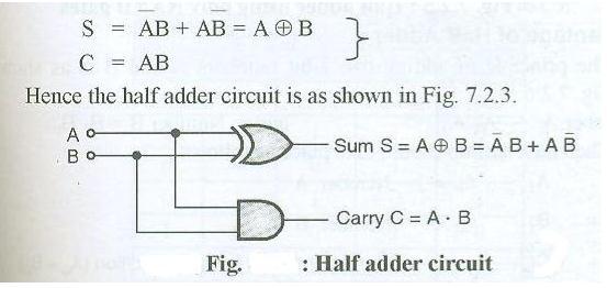
10 Page 10 of 33


11 e) Realize F1 = Σm ( 0, 2, 4, 6 ) F2 = Σm ( 1, 3, 5 ) using Demultiplexer. Ans:- ( Each realisation- 2 mks) f) Draw and explain S. R. and FlipFlop using NAND gate along with truth table. Ans:- ( Diagram- 2 mks, truth table 1 mks, explanation-1 mks) Description- Page 11 of 33
 For S=1, R=0, o/p of flipflop sets (Q=1) For S=R=1, o/p of flipflop is forbidden or not allowed as Q= Q. 3.")
12 Description/explanation- As shown in the truth table, For both inputs S=R= 0, o/p of flipflop remains unchanged. For S=0, R=1, o/p of flipflop resets (Q=0) For S=1, R=0, o/p of flipflop sets (Q=1) For S=R=1, o/p of flipflop is forbidden or not allowed as Q= Q. 3. Attempt any FOUR of the following: 16 a) Draw and explain working of R-2R DAC. Ans:- (Diagram 2mks, explanation-2 mks) Page 12 of 33
13 b) State different type of ROM and explain any one. Ans:- (Types- 2 mks, any one explanation-2 mks) Page 13 of 33


 Page")
14 OR c) Draw circuit diagram of TTL NAND gate and explain its working. Ans:- ( Diagram- 2 mks, truth table- 1 mks, explanation- 1 mks) Page 14 of 33

15 Page 15 of 33
2 (1001)2 (ii) (1000)2 ( 1001)2 Page 16")
16 d) Subtract using 2 s complement method (i) (1110)2 (1001)2 (ii) (1000)2 ( 1001)2 Page 16 of 33
 Page 17 of")
17 Ans:- ( Each proper stepwise solving- 2 mks each) Page 17 of 33


18 e) Draw Master Salve JF FlipFlop and write its truth table. Ans:- ( Diagram- 2 mks, truth table- 2 mks) Page 18 of 33
 Truth Table 4.")
19 f) Design MOD-6 Counter using IC 7490 and write its truth table. Ans:- ( Diagram- 2 mks, Truth table- 2 mks) Truth Table 4. Attempt any FOUR of the following: 16 Page 19 of 33
20 a) Describe working of SISO shift Register with proper circuit diagram. Ans:- (Diagram- 2 mks, truth table 1 mks, describe/explain in short 1 mks,waveform not compulsory, can be considered) Description-As shown a 4 bit SISO shift register consists of 4 D flipflop, data is fed from first flipflop and on application of clock pulses the data is shifted from first flipflop to the last flipflop,working as serial in and serial out shift register. Let the data be The truth table and timing diagram ( optional) is as shown below- Truth Table Page 20 of 33

 Ans:- ( Any 4 relevant")
21 Timing diagram-( optional) b) Compare combinational and sequential circuit. (Four points) Ans:- ( Any 4 relevant comparison- 4 mks) Page 21 of 33


 d) Explain")
22 c) Compare : (i) Volatile with Non-Volatile memory. (ii) SRAM with DRAM memory. Ans:- Volatile with Non-Volatile memory (any 2 points-2 mks) SRAM with DRAM memory ( any 2 points- 2 mks) d) Explain working of single slope ADC with diagram. Page 22 of 33

23 Page 23 of 33
 Ans :- ( Identification- 2 mks, operation with truth table as working 2 mks) Identification- The given circuit is")

24 e) Identity the given circuit and explain its working. (Refer Figure No. 1) Ans :- ( Identification- 2 mks, operation with truth table as working 2 mks) Identification- The given circuit is Ring Counter. Operation- As shown D1=1, with clock pulses applied the data 1 shifts as shown in the truth table- ( waveforms are optional, can be considered) f) Draw and explain working of 4-bit Weighted Register DAC Circuit. Ans:- ( Diagram- 2 mks, explanation-2 mks) Page 24 of 33


25 5. Attempt any FOUR of the following: 16 Page 25 of 33
 Basic gate b) Prove : (i) A + AB = A (ii) A + B + C = ABC Ans:- ( Each proper solution 2mks) c) Classify memories and Identify the IC (i) IC 2716 (ii) IC 7481 Ans:- (")
26 a) Compare TTL logic family with CMOS w.r.t. to (i) Propagation delay. (ii) Power dissipation (iii) Fan-out. (iv) Basic gate b) Prove : (i) A + AB = A (ii) A + B + C = ABC Ans:- ( Each proper solution 2mks) c) Classify memories and Identify the IC (i) IC 2716 (ii) IC 7481 Ans:- ( Classification- 2 mks, identification- 1 mks each) Page 26 of 33
 Design and draw 16:1")
 Truth")
27 Identification IC K bit, UV EEPROM IC bit Bipolar RAM d) Design and draw 16:1 MUX using 8:1 MUX (Multiplex). Ans:- (Diagram- 2mks, truth table-2 mks) Truth table Page 27 of 33
 A priority encoder is a special type of encoder that responds to just one input accordance with some")
28 e) What is priority encodes? How is Demultiplex used as Decoder? Ans:- ( Priority encoder, diagram can be considered -2 mks, Demux as decoder- 2mks for diagram) A priority encoder is a special type of encoder that responds to just one input accordance with some priority system among all those that may be applied simultaneously high. For two or more inputs are 1 at the same time, then input with highest priority will be considered. Page 28 of 33


 Page")
29 f) Draw block diagram of successive approximation type ADC and write its advantages Ans:- ( Block diagram- 2 mks, 2 advantages- 2 mks) Page 29 of 33
 Compare weighted resistor and R-2R methods of DAC.")
 Y = AB + BC (ii) Y = ABC + B Ans:-( Each conversion and proper answer -2 mks each) c) Minimize y = Σm (0, 5, 2, 8, 7, 10, 15, 13 )")
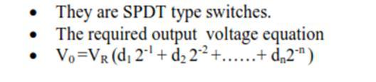
30 Advantages (any 2) 1. High speed of conversion 2. Produce n bit of A to D conversion with only n clock pulses. 3. Constant conversion time. 6. Attempt any FOUR of the following 16 a) Compare weighted resistor and R-2R methods of DAC. Ans:- ( Relevant 4 points- 4 mks) b) Write std SOP equation of given logical equation. (i) Y = AB + BC (ii) Y = ABC + B Ans:-( Each conversion and proper answer -2 mks each) c) Minimize y = Σm (0, 5, 2, 8, 7, 10, 15, 13 ) using k-map. Ans:- ( Proper K-map with correct minimized equation- 4 mks) Page 30 of 33
 ( Note 2 advantages and 2 applications of MUX and DEMUX each can be given separately- 1 mks")
31 d) Write Advantages of MUX and DEMUX.State their applications. Ans:- ( 2 advantages of MUX and DEMUX- 2 mks, 2 applications of MUX- 1 mks, 2 applications of DEMUX- 1 mks) ( Note 2 advantages and 2 applications of MUX and DEMUX each can be given separately- 1 mks each) Advantages- Applications- 1. Communication System 2. Computer Memory 3. Telephone Network 4. Transmission from the Computer System of a Satellite 5. TV Cable System Page 31 of 33


32 e) Identify the given circuit and write its truth table Diagram below (Refer Figure No.2) Ans:- ( Identification- 2 mks, truth table-2 mks) The given circuit is a MUX tree - 8:1 MUX using 4: 1 Mux. Truth Table- f) (i) Draw circuit diagram of MOD 10 counter using T-FF. Ans:- ( Proper detailed diagram-2 mks) Page 32 of 33
 Page 33 of")
33 (ii) Identify the function of 1) IC ) IC 0890 Ans:- ( Proper identification -1 mks each) Page 33 of 33
MAHARASHTRA STATE BOARD OF TECHNICAL EDUCATION (Autonomous) (ISO/IEC Certified) State any two Boolean laws. (Any 2 laws 1 mark each)
 (ISO/IEC Certified) State any two Boolean laws. (Any 2 laws 1 mark each)") Subject Code: 17333 Model Answer Page 1/ 27 Important Instructions to examiners: 1) The answers should be examined by key words and not as word-to-word as given in the model answer scheme. 2) The model
Subject Code: 17333 Model Answer Page 1/ 27 Important Instructions to examiners: 1) The answers should be examined by key words and not as word-to-word as given in the model answer scheme. 2) The model
Sample Test Paper - I
 Scheme G Sample Test Paper - I Course Name : Computer Engineering Group Marks : 25 Hours: 1 Hrs. Q.1) Attempt any THREE: 09 Marks a) Define i) Propagation delay ii) Fan-in iii) Fan-out b) Convert the following:
MAHARASHTRA STATE BOARD OF TECHNICAL EDUCATION (Autonomous) (ISO/IEC Certified)
 (ISO/IEC Certified)") WINTER 17 EXAMINATION Subject Name: Digital Techniques Model Answer Subject Code: 17333 Important Instructions to examiners: 1) The answers should be examined by key words and not as word-to-word as given
WINTER 17 EXAMINATION Subject Name: Digital Techniques Model Answer Subject Code: 17333 Important Instructions to examiners: 1) The answers should be examined by key words and not as word-to-word as given
on candidate s understanding. 7) For programming language papers, credit may be given to any other program based on equivalent concept.
 For programming language papers, credit may be given to any other program based on equivalent concept.") WINTER 17 EXAMINATION Subject Name: Digital Techniques Model Answer Subject Code: 17333 Important Instructions to examiners: 1) The answers should be examined by key words and not as word-to-word as given
WINTER 17 EXAMINATION Subject Name: Digital Techniques Model Answer Subject Code: 17333 Important Instructions to examiners: 1) The answers should be examined by key words and not as word-to-word as given
S.Y. Diploma : Sem. III [CO/CM/IF/CD/CW] Digital Techniques
![S.Y. Diploma : Sem. III [CO/CM/IF/CD/CW] Digital Techniques](/thumbs/90/103932933.jpg "S.Y. Diploma : Sem. III [CO/CM/IF/CD/CW] Digital Techniques") S.Y. Diploma : Sem. III [CO/CM/IF/CD/CW] Digital Techniques Time: 3 Hrs.] Prelim Question Paper Solution [Marks : 100 Q.1(a) Attempt any SIX of the following : [12] Q.1(a) (i) Derive AND gate and OR gate
S.Y. Diploma : Sem. III [CO/CM/IF/CD/CW] Digital Techniques Time: 3 Hrs.] Prelim Question Paper Solution [Marks : 100 Q.1(a) Attempt any SIX of the following : [12] Q.1(a) (i) Derive AND gate and OR gate
MAHARASHTRA STATE BOARD OF TECHNICAL EDUCATION (Autonomous) (ISO/IEC Certified) SUMMER 14 EXAMINATION Model Answer
 (ISO/IEC Certified) SUMMER 14 EXAMINATION Model Answer") MAHARASHTRA STATE BOARD OF TECHNICAL EDUCATION (Autonomous) (ISO/IEC 27001 2005 Certified) SUMMER 14 EXAMINATION Model Answer Subject Code : 17320 Page No: 1/34 Important Instructions to examiners: 1)
MAHARASHTRA STATE BOARD OF TECHNICAL EDUCATION (Autonomous) (ISO/IEC 27001 2005 Certified) SUMMER 14 EXAMINATION Model Answer Subject Code : 17320 Page No: 1/34 Important Instructions to examiners: 1)
MAHARASHTRA STATE BOARD OF TECHNICAL EDUCATION
 MAHARASHTRA STATE BOARD OF TECHNICAL EDUCATION (Autonomous) (ISO/IEC - 27001-2005 Certified) Subject Code: 12069 SUMMER 13 EXAMINATION Model Answer Important Instructions to examiners: 1) The answers should
 vidyarthiplus.com vidyarthiplus.com vidyarthiplus.com ANNA UNIVERSITY- COMBATORE B.E./ B.TECH. DEGREE EXAMINATION - JUNE 2009. ELECTRICAL & ELECTONICS ENGG. - FOURTH SEMESTER DIGITAL LOGIC CIRCUITS PART-A
S.Y. Diploma : Sem. III [DE/ED/EI/EJ/EN/ET/EV/EX/IC/IE/IS/IU/MU] Principles of Digital Techniques
![S.Y. Diploma : Sem. III [DE/ED/EI/EJ/EN/ET/EV/EX/IC/IE/IS/IU/MU] Principles of Digital Techniques](/thumbs/82/86792063.jpg "S.Y. Diploma : Sem. III [DE/ED/EI/EJ/EN/ET/EV/EX/IC/IE/IS/IU/MU] Principles of Digital Techniques") S.Y. Diploma : Sem. III [DE/ED/EI/EJ/EN/ET/EV/EX/IC/IE/IS/IU/MU] Principles of Digital Techniques Time: 3 Hrs.] Prelim Question Paper Solution [Marks : 100 Q.1(a) Attempt any SIX of the following : [12]
S.Y. Diploma : Sem. III [DE/ED/EI/EJ/EN/ET/EV/EX/IC/IE/IS/IU/MU] Principles of Digital Techniques Time: 3 Hrs.] Prelim Question Paper Solution [Marks : 100 Q.1(a) Attempt any SIX of the following : [12]
SUMMER 18 EXAMINATION Subject Name: Principles of Digital Techniques Model Answer Subject Code:
 Important Instructions to examiners: 1) The answers should be examined by key words and not as word-to-word as given in the model answer scheme. 2) The model answer and the answer written by candidate
KUMARAGURU COLLEGE OF TECHNOLOGY COIMBATORE
 Estd-1984 KUMARAGURU COLLEGE OF TECHNOLOGY COIMBATORE 641 006 QUESTION BANK UNIT I PART A ISO 9001:2000 Certified 1. Convert (100001110.010) 2 to a decimal number. 2. Find the canonical SOP for the function
DE58/DC58 LOGIC DESIGN DEC 2014
 Q.2 a. In a base-5 number system, 3 digit representations is used. Find out (i) Number of distinct quantities that can be represented.(ii) Representation of highest decimal number in base-5. Since, r=5
Reg. No. Question Paper Code : B.E./B.Tech. DEGREE EXAMINATION, NOVEMBER/DECEMBER Second Semester. Computer Science and Engineering
 Sp 6 Reg. No. Question Paper Code : 27156 B.E./B.Tech. DEGREE EXAMINATION, NOVEMBER/DECEMBER 2015. Second Semester Computer Science and Engineering CS 6201 DIGITAL PRINCIPLES AND SYSTEM DESIGN (Common
SIR C.R.REDDY COLLEGE OF ENGINEERING ELURU DIGITAL INTEGRATED CIRCUITS (DIC) LABORATORY MANUAL III / IV B.E. (ECE) : I - SEMESTER
 LABORATORY MANUAL III / IV B.E. (ECE) : I - SEMESTER") SIR C.R.REDDY COLLEGE OF ENGINEERING ELURU 534 007 DIGITAL INTEGRATED CIRCUITS (DIC) LABORATORY MANUAL III / IV B.E. (ECE) : I - SEMESTER DEPARTMENT OF ELECTRONICS AND COMMUNICATION ENGINEERING DIGITAL
SIR C.R.REDDY COLLEGE OF ENGINEERING ELURU 534 007 DIGITAL INTEGRATED CIRCUITS (DIC) LABORATORY MANUAL III / IV B.E. (ECE) : I - SEMESTER DEPARTMENT OF ELECTRONICS AND COMMUNICATION ENGINEERING DIGITAL
Chapter 4. Combinational: Circuits with logic gates whose outputs depend on the present combination of the inputs. elements. Dr.
 Chapter 4 Dr. Panos Nasiopoulos Combinational: Circuits with logic gates whose outputs depend on the present combination of the inputs. Sequential: In addition, they include storage elements Combinational
ELECTRONICS & COMMUNICATION ENGINEERING PROFESSIONAL ETHICS AND HUMAN VALUES
 EC 216(R-15) Total No. of Questions :09] [Total No. of Pages : 02 II/IV B.Tech. DEGREE EXAMINATIONS, DECEMBER- 2016 First Semester ELECTRONICS & COMMUNICATION ENGINEERING PROFESSIONAL ETHICS AND HUMAN
Digital Electronics Circuits 2017
 JSS SCIENCE AND TECHNOLOGY UNIVERSITY Digital Electronics Circuits (EC37L) Lab in-charge: Dr. Shankraiah Course outcomes: After the completion of laboratory the student will be able to, 1. Simplify, design
WORKBOOK. Try Yourself Questions. Electrical Engineering Digital Electronics. Detailed Explanations of
 27 WORKBOOK Detailed Eplanations of Try Yourself Questions Electrical Engineering Digital Electronics Number Systems and Codes T : Solution Converting into decimal number system 2 + 3 + 5 + 8 2 + 4 8 +
Vidyalankar S.E. Sem. III [CMPN] Digital Logic Design and Analysis Prelim Question Paper Solution
![Vidyalankar S.E. Sem. III [CMPN] Digital Logic Design and Analysis Prelim Question Paper Solution](/thumbs/90/103673562.jpg "Vidyalankar S.E. Sem. III [CMPN] Digital Logic Design and Analysis Prelim Question Paper Solution") . (a) (i) ( B C 5) H (A 2 B D) H S.E. Sem. III [CMPN] Digital Logic Design and Analysis Prelim Question Paper Solution ( B C 5) H (A 2 B D) H = (FFFF 698) H (ii) (2.3) 4 + (22.3) 4 2 2. 3 2. 3 2 3. 2 (2.3)
. (a) (i) ( B C 5) H (A 2 B D) H S.E. Sem. III [CMPN] Digital Logic Design and Analysis Prelim Question Paper Solution ( B C 5) H (A 2 B D) H = (FFFF 698) H (ii) (2.3) 4 + (22.3) 4 2 2. 3 2. 3 2 3. 2 (2.3)
PAST EXAM PAPER & MEMO N3 ABOUT THE QUESTION PAPERS:
 EKURHULENI TECH COLLEGE. No. 3 Mogale Square, Krugersdorp. Website: www. ekurhulenitech.co.za Email: info@ekurhulenitech.co.za TEL: 011 040 7343 CELL: 073 770 3028/060 715 4529 PAST EXAM PAPER & MEMO N3
Dept. of ECE, CIT, Gubbi Page 1
 Verification: 1) A.B = A + B 7404 7404 7404 A B A.B A.B 0 0 0 1 0 1 0 1 1 0 0 1 1 1 1 0 A B A B A + B 0 0 1 1 1 0 1 1 0 1 1 0 0 1 1 1 1 0 0 0 2) A+B = A. B 7404 7404 7404 A B A+B A+B 0 0 0 1 0 1 1 0 1
DIGITAL LOGIC CIRCUITS
 DIGITAL LOGIC CIRCUITS Introduction Logic Gates Boolean Algebra Map Specification Combinational Circuits Flip-Flops Sequential Circuits Memory Components Integrated Circuits Digital Computers 2 LOGIC GATES
Show that the dual of the exclusive-or is equal to its compliment. 7
 Darshan Institute of ngineering and Technology, Rajkot, Subject: Digital lectronics (2300) GTU Question ank Unit Group Questions Do as directed : I. Given that (6)0 = (00)x, find the value of x. II. dd
Logic. Combinational. inputs. outputs. the result. system can
 Digital Electronics Combinational Logic Functions Digital logic circuits can be classified as either combinational or sequential circuits. A combinational circuit is one where the output at any time depends
Philadelphia University Student Name: Student Number:
 Philadelphia University Student Name: Student Number: Faculty of Engineering Serial Number: Final Exam, First Semester: 2017/2018 Dept. of Computer Engineering Course Title: Logic Circuits Date: 29/01/2018
LOGIC CIRCUITS. Basic Experiment and Design of Electronics. Ho Kyung Kim, Ph.D.
 Basic Experiment and Design of Electronics LOGIC CIRCUITS Ho Kyung Kim, Ph.D. hokyung@pusan.ac.kr School of Mechanical Engineering Pusan National University Digital IC packages TTL (transistor-transistor
Boolean Algebra and Digital Logic 2009, University of Colombo School of Computing
 IT 204 Section 3.0 Boolean Algebra and Digital Logic Boolean Algebra 2 Logic Equations to Truth Tables X = A. B + A. B + AB A B X 0 0 0 0 3 Sum of Products The OR operation performed on the products of
Number System. Decimal to binary Binary to Decimal Binary to octal Binary to hexadecimal Hexadecimal to binary Octal to binary
 Number System Decimal to binary Binary to Decimal Binary to octal Binary to hexadecimal Hexadecimal to binary Octal to binary BOOLEAN ALGEBRA BOOLEAN LOGIC OPERATIONS Logical AND Logical OR Logical COMPLEMENTATION
Vidyalankar S.E. Sem. III [EXTC] Digital Electronics Prelim Question Paper Solution ABCD ABCD ABCD ABCD ABCD ABCD ABCD ABCD = B
![Vidyalankar S.E. Sem. III [EXTC] Digital Electronics Prelim Question Paper Solution ABCD ABCD ABCD ABCD ABCD ABCD ABCD ABCD = B](/thumbs/84/91058397.jpg "Vidyalankar S.E. Sem. III [EXTC] Digital Electronics Prelim Question Paper Solution ABCD ABCD ABCD ABCD ABCD ABCD ABCD ABCD = B") . (a). (b). (c) S.E. Sem. III [EXTC] igital Electronics Prelim Question Paper Solution ABC ABC ABC ABC ABC ABC ABC ABC = B LHS = ABC ABC ABC ABC ABC ABC ABC ABC But ( ) = = ABC( ) ABC( ) ABC( ) ABC( )
. (a). (b). (c) S.E. Sem. III [EXTC] igital Electronics Prelim Question Paper Solution ABC ABC ABC ABC ABC ABC ABC ABC = B LHS = ABC ABC ABC ABC ABC ABC ABC ABC But ( ) = = ABC( ) ABC( ) ABC( ) ABC( )
Philadelphia University Student Name: Student Number:
 Philadelphia University Student Name: Student Number: Faculty of Engineering Serial Number: Final Exam, Second Semester: 2015/2016 Dept. of Computer Engineering Course Title: Logic Circuits Date: 08/06/2016
Design of Sequential Circuits
 Design of Sequential Circuits Seven Steps: Construct a state diagram (showing contents of flip flop and inputs with next state) Assign letter variables to each flip flop and each input and output variable
Department of Electrical & Electronics EE-333 DIGITAL SYSTEMS
 Department of Electrical & Electronics EE-333 DIGITAL SYSTEMS 1) Given the two binary numbers X = 1010100 and Y = 1000011, perform the subtraction (a) X -Y and (b) Y - X using 2's complements. a) X = 1010100
Unit II Chapter 4:- Digital Logic Contents 4.1 Introduction... 4
 Unit II Chapter 4:- Digital Logic Contents 4.1 Introduction... 4 4.1.1 Signal... 4 4.1.2 Comparison of Analog and Digital Signal... 7 4.2 Number Systems... 7 4.2.1 Decimal Number System... 7 4.2.2 Binary
Introduction to Computer Engineering. CS/ECE 252, Fall 2012 Prof. Guri Sohi Computer Sciences Department University of Wisconsin Madison
 Introduction to Computer Engineering CS/ECE 252, Fall 2012 Prof. Guri Sohi Computer Sciences Department University of Wisconsin Madison Chapter 3 Digital Logic Structures Slides based on set prepared by
CHW 261: Logic Design
 CHW 26: Logic Design Instructors: Prof. Hala Zayed Dr. Ahmed Shalaby http://www.bu.edu.eg/staff/halazayed4 http://bu.edu.eg/staff/ahmedshalaby4# Slide Digital Fundamentals Digital Concepts Slide 2 What?
EE40 Lec 15. Logic Synthesis and Sequential Logic Circuits
 EE40 Lec 15 Logic Synthesis and Sequential Logic Circuits Prof. Nathan Cheung 10/20/2009 Reading: Hambley Chapters 7.4-7.6 Karnaugh Maps: Read following before reading textbook http://www.facstaff.bucknell.edu/mastascu/elessonshtml/logic/logic3.html
SAU1A FUNDAMENTALS OF DIGITAL COMPUTERS
 SAU1A FUNDAMENTALS OF DIGITAL COMPUTERS Unit : I - V Unit : I Overview Fundamentals of Computers Characteristics of Computers Computer Language Operating Systems Generation of Computers 2 Definition of
UNIVERSITI TENAGA NASIONAL. College of Information Technology
 UNIVERSITI TENAGA NASIONAL College of Information Technology BACHELOR OF COMPUTER SCIENCE (HONS.) FINAL EXAMINATION SEMESTER 2 2012/2013 DIGITAL SYSTEMS DESIGN (CSNB163) January 2013 Time allowed: 3 hours
MAHALAKSHMI ENGINEERING COLLEGE TIRUCHIRAPALLI
 DEPARTMENT: ECE MAHALAKSHMI ENGINEERING COLLEGE TIRUCHIRAPALLI 6 QUESTION BANK SUBJECT NAME: DIGITAL ELECTRONICS UNIT : Design of Sequential Circuits PART A ( Marks). Draw the logic diagram 4: Multiplexer.(AUC
LOGIC CIRCUITS. Basic Experiment and Design of Electronics
 Basic Experiment and Design of Electronics LOGIC CIRCUITS Ho Kyung Kim, Ph.D. hokyung@pusan.ac.kr School of Mechanical Engineering Pusan National University Outline Combinational logic circuits Output
Analog & Digital Electronics Laboratory. Code - CS391. Lab Manual
 Analog & Digital Electronics Laboratory Code - CS391 Lab Manual EXPERIMENT: 1 LOGIC GATES AIM: To study and verify the truth table of logic gates LEARNING OBJECTIVE: Identify various ICs and their specification.
Fundamentals of Digital Design
 Fundamentals of Digital Design Digital Radiation Measurement and Spectroscopy NE/RHP 537 1 Binary Number System The binary numeral system, or base-2 number system, is a numeral system that represents numeric
DHANALAKSHMI COLLEGE OF ENGINEERING, CHENNAI DEPARTMENT OF COMPUTER SCIENCE AND ENGINEERING CS6201 DIGITAL PRINCIPLES AND SYSTEM DESIGN
 DHANALAKSHMI COLLEGE OF ENGINEERING, CHENNAI DEPARTMENT OF COMPUTER SCIENCE AND ENGINEERING CS6201 DIGITAL PRINCIPLES AND SYSTEM DESIGN UNIT I : BOOLEAN ALGEBRA AND LOGIC GATES PART - A (2 MARKS) Number
Combinational Logic. By : Ali Mustafa
 Combinational Logic By : Ali Mustafa Contents Adder Subtractor Multiplier Comparator Decoder Encoder Multiplexer How to Analyze any combinational circuit like this? Analysis Procedure To obtain the output
Unit 3 Session - 9 Data-Processing Circuits
 Objectives Unit 3 Session - 9 Data-Processing Design of multiplexer circuits Discuss multiplexer applications Realization of higher order multiplexers using lower orders (multiplexer trees) Introduction
Delhi Noida Bhopal Hyderabad Jaipur Lucknow Indore Pune Bhubaneswar Kolkata Patna Web: Ph:
 Serial : S_CS_C_Digital Logic_588 Delhi Noida hopal Hyderabad Jaipur Lucknow Indore Pune hubaneswar Kolkata Patna Web: E-mail: info@madeeasy.in Ph: -56 CLASS TEST 8-9 COMPUTER SCIENCE & IT Subject : Digital
Digital Logic Design ENEE x. Lecture 14
 Digital Logic Design ENEE 244-010x Lecture 14 Announcements Homework 6 due today Agenda Last time: Binary Adders and Subtracters (5.1, 5.1.1) Carry Lookahead Adders (5.1.2, 5.1.3) This time: Decimal Adders
TYPICAL QUESTIONS & ANSWERS
 TYPICAL QUESTIONS & ANSWERS PART - I OJECTIVE TYPE QUESTIONS Each Question carries 2 marks. Choose correct or the best alternative in the following: Q.1 The NAN gate output will be low if the two inputs
ELCT201: DIGITAL LOGIC DESIGN
 ELCT201: DIGITAL LOGIC DESIGN Dr. Eng. Haitham Omran, haitham.omran@guc.edu.eg Dr. Eng. Wassim Alexan, wassim.joseph@guc.edu.eg Lecture 5 Following the slides of Dr. Ahmed H. Madian ذو الحجة 1438 ه Winter
COMBINATIONAL LOGIC FUNCTIONS
 COMBINATIONAL LOGIC FUNCTIONS Digital logic circuits can be classified as either combinational or sequential circuits. A combinational circuit is one where the output at any time depends only on the present
S.E. Sem. III [ETRX] Digital Circuit Design. t phl. Fig.: Input and output voltage waveforms to define propagation delay times.
![S.E. Sem. III [ETRX] Digital Circuit Design. t phl. Fig.: Input and output voltage waveforms to define propagation delay times.](/thumbs/93/111090909.jpg "S.E. Sem. III [ETRX] Digital Circuit Design. t phl. Fig.: Input and output voltage waveforms to define propagation delay times.") S.E. Sem. III [ETRX] Digital ircuit Design Time : 3 Hrs.] Prelim Paper Solution [Marks : 80. Solve following : [20].(a) Explain characteristics of logic families. [5] haracteristics of logic families are
S.E. Sem. III [ETRX] Digital ircuit Design Time : 3 Hrs.] Prelim Paper Solution [Marks : 80. Solve following : [20].(a) Explain characteristics of logic families. [5] haracteristics of logic families are
Cs302 Quiz for MID TERM Exam Solved
 Question # 1 of 10 ( Start time: 01:30:33 PM ) Total Marks: 1 Caveman used a number system that has distinct shapes: 4 5 6 7 Question # 2 of 10 ( Start time: 01:31:25 PM ) Total Marks: 1 TTL based devices
DIGITAL LOGIC CIRCUITS
 DIGITAL LOGIC CIRCUITS Introduction Logic Gates Boolean Algebra Map Specification Combinational Circuits Flip-Flops Sequential Circuits Memor Components Integrated Circuits BASIC LOGIC BLOCK - GATE - Logic
Function of Combinational Logic ENT263
 Function of Combinational Logic ENT263 Chapter Objectives Distinguish between half-adder and full-adder Use BCD-to-7-segment decoders in display systems Apply multiplexer in data selection Use decoders
Vidyalankar S.E. Sem. III [ETRX] Digital Circuits and Design Prelim Question Paper Solution
![Vidyalankar S.E. Sem. III [ETRX] Digital Circuits and Design Prelim Question Paper Solution](/thumbs/79/79145081.jpg "Vidyalankar S.E. Sem. III [ETRX] Digital Circuits and Design Prelim Question Paper Solution") S.E. Sem. III [ETRX] Digital Circuits and Design Prelim uestion Paper Solution. (a) Static Hazard Static hazards have two cases: static and static. static- hazard exists when the output variable should
S.E. Sem. III [ETRX] Digital Circuits and Design Prelim uestion Paper Solution. (a) Static Hazard Static hazards have two cases: static and static. static- hazard exists when the output variable should
Digital System Design Combinational Logic. Assoc. Prof. Pradondet Nilagupta
 Digital System Design Combinational Logic Assoc. Prof. Pradondet Nilagupta pom@ku.ac.th Acknowledgement This lecture note is modified from Engin112: Digital Design by Prof. Maciej Ciesielski, Prof. Tilman
King Fahd University of Petroleum and Minerals College of Computer Science and Engineering Computer Engineering Department
 King Fahd University of Petroleum and Minerals College of Computer Science and Engineering Computer Engineering Department Page 1 of 13 COE 202: Digital Logic Design (3-0-3) Term 112 (Spring 2012) Final
MAHALAKSHMI ENGINEERING COLLEGE TIRUCHIRAPALLI
 MAHALAKSHMI ENGINEERING COLLEGE TIRUCHIRAPALLI 6 DEPARTMENT: EEE QUESTION BANK SUBJECT NAME: DIGITAL LOGIC CIRCUITS SUBJECT CODE: EE55 SEMESTER IV UNIT : Design of Synchronous Sequential Circuits PART
04. What is the Mod number of the counter circuit shown below? Assume initially reset.
 . Which of the following is the state diagram for the Meale machine shown below. 4. What is the Mod number of the counter circuit shown below? Assume initiall reset. input CLK D output D D a. b. / / /
Lecture 22 Chapters 3 Logic Circuits Part 1
 Lecture 22 Chapters 3 Logic Circuits Part 1 LC-3 Data Path Revisited How are the components Seen here implemented? 5-2 Computing Layers Problems Algorithms Language Instruction Set Architecture Microarchitecture
Digital Electronics Final Examination. Part A
 Digital Electronics Final Examination Part A Spring 2009 Student Name: Date: Class Period: Total Points: /50 Converted Score: /40 Page 1 of 13 Directions: This is a CLOSED BOOK/CLOSED NOTES exam. Select
Section 3: Combinational Logic Design. Department of Electrical Engineering, University of Waterloo. Combinational Logic
 Section 3: Combinational Logic Design Major Topics Design Procedure Multilevel circuits Design with XOR gates Adders and Subtractors Binary parallel adder Decoders Encoders Multiplexers Programmed Logic
( c) Give logic symbol, Truth table and circuit diagram for a clocked SR flip-flop. A combinational circuit is defined by the function
 Give logic symbol, Truth table and circuit diagram for a clocked SR flip-flop. A combinational circuit is defined by the function") Question Paper Digital Electronics (EE-204-F) MDU Examination May 2015 1. (a) represent (32)10 in (i) BCD 8421 code (ii) Excess-3 code (iii) ASCII code (b) Design half adder using only NAND gates. ( c)
Question Paper Digital Electronics (EE-204-F) MDU Examination May 2015 1. (a) represent (32)10 in (i) BCD 8421 code (ii) Excess-3 code (iii) ASCII code (b) Design half adder using only NAND gates. ( c)
INSTITUTEOFAERONAUTICALENGINEERING (Autonomous) Dundigal, Hyderabad
 Dundigal, Hyderabad") INSTITUTEOFAERONAUTICALENGINEERING (Autonomous) Dundigal, Hyderabad - 50004 COMPUTER SCIENCE AND ENGINEERING TUTORIAL QUESTION BANK Course Name Course Code Class Branch DIGITAL LOGIC DESIGN A040 II B.
INSTITUTEOFAERONAUTICALENGINEERING (Autonomous) Dundigal, Hyderabad - 50004 COMPUTER SCIENCE AND ENGINEERING TUTORIAL QUESTION BANK Course Name Course Code Class Branch DIGITAL LOGIC DESIGN A040 II B.
Chapter 7. Sequential Circuits Registers, Counters, RAM
 Chapter 7. Sequential Circuits Registers, Counters, RAM Register - a group of binary storage elements suitable for holding binary info A group of FFs constitutes a register Commonly used as temporary storage
A B D 1 Y D 2 D 3. Truth table for 4 to 1 MUX: A B Y 0 0 D D D D 3
 . What is a multiplexer? esign a 4 to multiplexer using logic gates. Write the truth table and explain its working principle. Answer: is a circuit with many inputs but only one output. esigning of 4 to
3 Logic Function Realization with MSI Circuits
 3 Logic Function Realization with MSI Circuits Half adder A half-adder is a combinational circuit with two binary inputs (augund and addend bits) and two binary outputs (sum and carry bits). It adds the
Schedule. ECEN 301 Discussion #25 Final Review 1. Date Day Class No. 1 Dec Mon 25 Final Review. Title Chapters HW Due date. Lab Due date.
 Schedule Date Day Class No. Dec Mon 25 Final Review 2 Dec Tue 3 Dec Wed 26 Final Review Title Chapters HW Due date Lab Due date LAB 8 Exam 4 Dec Thu 5 Dec Fri Recitation HW 6 Dec Sat 7 Dec Sun 8 Dec Mon
Introduction to Computer Engineering. CS/ECE 252, Spring 2017 Rahul Nayar Computer Sciences Department University of Wisconsin Madison
 Introduction to Computer Engineering CS/ECE 252, Spring 2017 Rahul Nayar Computer Sciences Department University of Wisconsin Madison Chapter 3 Digital Logic Structures Slides based on set prepared by
ALU A functional unit
 ALU A functional unit that performs arithmetic operations such as ADD, SUB, MPY logical operations such as AND, OR, XOR, NOT on given data types: 8-,16-,32-, or 64-bit values A n-1 A n-2... A 1 A 0 B n-1
Written exam for IE1204/5 Digital Design with solutions Thursday 29/
 Written exam for IE4/5 Digital Design with solutions Thursday 9/ 5 9.-. General Information Examiner: Ingo Sander. Teacher: William Sandqvist phone 8-794487 Exam text does not have to be returned when
Save from: cs. Logic design 1 st Class أستاذ المادة: د. عماد
 Save from: www.uotiq.org/dep cs Logic design 1 st Class أستاذ المادة: د. عماد استاذة المادة: م.م ميساء Contents Lectured One: Number system operation 1- Decimal numbers. 2- Binary numbers. 3- Octal numbers.
Unit 7 Sequential Circuits (Flip Flop, Registers)
") College of Computer and Information Sciences Department of Computer Science CSC 220: Computer Organization Unit 7 Sequential Circuits (Flip Flop, Registers) 2 SR Flip-Flop The SR flip-flop, also known
College of Computer and Information Sciences Department of Computer Science CSC 220: Computer Organization Unit 7 Sequential Circuits (Flip Flop, Registers) 2 SR Flip-Flop The SR flip-flop, also known
PG - TRB UNIT-X- DIGITAL ELECTRONICS. POLYTECHNIC-TRB MATERIALS
 SRIMAAN COACHING CENTRE-PG-TRB-PHYSICS- DIGITAL ELECTRONICS-STUDY MATERIAL-CONTACT: 8072230063 SRIMAAN PG - TRB PHYSICS UNIT-X- DIGITAL ELECTRONICS POLYTECHNIC-TRB MATERIALS MATHS/COMPUTER SCIENCE/IT/ECE/EEE
Chapter 7 Logic Circuits
 Chapter 7 Logic Circuits Goal. Advantages of digital technology compared to analog technology. 2. Terminology of Digital Circuits. 3. Convert Numbers between Decimal, Binary and Other forms. 5. Binary
Solution (a) We can draw Karnaugh maps for NS1, NS0 and OUT:
 We can draw Karnaugh maps for NS1, NS0 and OUT:") DIGITAL ELECTRONICS II Revision Examples 7 Exam Format Q compulsory + any out of Q, Q, Q4. Q has 5 parts worth 8% each, Q,,4 are worth %. Revision Lectures Three revision lectures will be given on the
DIGITAL ELECTRONICS II Revision Examples 7 Exam Format Q compulsory + any out of Q, Q, Q4. Q has 5 parts worth 8% each, Q,,4 are worth %. Revision Lectures Three revision lectures will be given on the
CHAPTER 7. Exercises 17/ / /2 2 0
 CHAPTER 7 Exercises E7. (a) For the whole part, we have: Quotient Remainders 23/2 /2 5 5/2 2 2/2 0 /2 0 Reading the remainders in reverse order, we obtain: 23 0 = 0 2 For the fractional part we have 2
Combinational Logic. Mantıksal Tasarım BBM231. section instructor: Ufuk Çelikcan
 Combinational Logic Mantıksal Tasarım BBM23 section instructor: Ufuk Çelikcan Classification. Combinational no memory outputs depends on only the present inputs expressed by Boolean functions 2. Sequential
Digital Logic. CS211 Computer Architecture. l Topics. l Transistors (Design & Types) l Logic Gates. l Combinational Circuits.
 l Logic Gates. l Combinational Circuits.") CS211 Computer Architecture Digital Logic l Topics l Transistors (Design & Types) l Logic Gates l Combinational Circuits l K-Maps Figures & Tables borrowed from:! http://www.allaboutcircuits.com/vol_4/index.html!
CS211 Computer Architecture Digital Logic l Topics l Transistors (Design & Types) l Logic Gates l Combinational Circuits l K-Maps Figures & Tables borrowed from:! http://www.allaboutcircuits.com/vol_4/index.html!
S.Y. Diploma : Sem. III [CO/CM/IF/CD/CW] Digital Techniques s complement 2 s complement 1 s complement
![S.Y. Diploma : Sem. III [CO/CM/IF/CD/CW] Digital Techniques s complement 2 s complement 1 s complement](/thumbs/80/82077570.jpg "S.Y. Diploma : Sem. III [CO/CM/IF/CD/CW] Digital Techniques s complement 2 s complement 1 s complement") S.Y. Diploma : Sem. III [CO/CM/IF/CD/CW] Digital Techniques Time: 3 Hrs.] Prelim Question Paper Solution [Marks : Q.(a) (i) () (2) s COMPLEMENT s COMPLEMENT 2s COMPLEMENT 2s COMPLEMENT + Q.(a) (ii) ()
S.Y. Diploma : Sem. III [CO/CM/IF/CD/CW] Digital Techniques Time: 3 Hrs.] Prelim Question Paper Solution [Marks : Q.(a) (i) () (2) s COMPLEMENT s COMPLEMENT 2s COMPLEMENT 2s COMPLEMENT + Q.(a) (ii) ()
Sequential vs. Combinational
 Sequential Circuits Sequential vs. Combinational Combinational Logic: Output depends only on current input TV channel selector (-9) inputs system outputs Sequential Logic: Output depends not only on current
ECEN 248: INTRODUCTION TO DIGITAL SYSTEMS DESIGN. Week 9 Dr. Srinivas Shakkottai Dept. of Electrical and Computer Engineering
 ECEN 248: INTRODUCTION TO DIGITAL SYSTEMS DESIGN Week 9 Dr. Srinivas Shakkottai Dept. of Electrical and Computer Engineering TIMING ANALYSIS Overview Circuits do not respond instantaneously to input changes
Systems I: Computer Organization and Architecture
 Systems I: Computer Organization and Architecture Lecture 6 - Combinational Logic Introduction A combinational circuit consists of input variables, logic gates, and output variables. The logic gates accept
ECE 341. Lecture # 3
 ECE 341 Lecture # 3 Instructor: Zeshan Chishti zeshan@ece.pdx.edu October 7, 2013 Portland State University Lecture Topics Counters Finite State Machines Decoders Multiplexers Reference: Appendix A of
PART-A. 2. Expand ASCII and BCD ASCII American Standard Code for Information Interchange BCD Binary Coded Decimal
 PART-A 1. What is radix? Give the radix for binary, octal, decimal and hexadecimal Radix is the total number of digits used in a particular number system Binary - 2 (0,1) Octal - 8 (0 to 7) Decimal - 10
Z = F(X) Combinational circuit. A combinational circuit can be specified either by a truth table. Truth Table
 Combinational circuit. A combinational circuit can be specified either by a truth table. Truth Table") Lesson Objectives In this lesson, you will learn about What are combinational circuits Design procedure of combinational circuits Examples of combinational circuit design Combinational Circuits Logic circuit
Lesson Objectives In this lesson, you will learn about What are combinational circuits Design procedure of combinational circuits Examples of combinational circuit design Combinational Circuits Logic circuit
Written exam with solutions IE Digital Design Friday 21/
 Written exam with solutions IE204-5 Digital Design Friday 2/0 206 09.00-3.00 General Information Examiner: Ingo Sander. Teacher: Kista, William Sandvist tel 08-7904487, Elena Dubrova phone 08-790 4 4 Exam
Design of Combinational Logic
 Pune Vidyarthi Griha s COLLEGE OF ENGINEERING, NASHIK 3. Design of Combinational Logic By Prof. Anand N. Gharu (Assistant Professor) PVGCOE Computer Dept.. 30 th June 2017 CONTENTS :- 1. Code Converter
Digital Electronics II Mike Brookes Please pick up: Notes from the front desk
 NOTATION.PPT(10/8/2010) 1.1 Digital Electronics II Mike Brookes Please pick up: Notes from the front desk 1. What does Digital mean? 2. Where is it used? 3. Why is it used? 4. What are the important features
3. Complete the following table of equivalent values. Use binary numbers with a sign bit and 7 bits for the value
 EGC22 Digital Logic Fundamental Additional Practice Problems. Complete the following table of equivalent values. Binary. Octal 35.77 33.23.875 29.99 27 9 64 Hexadecimal B.3 D.FD B.4C 2. Calculate the following
EECS150 - Digital Design Lecture 23 - FSMs & Counters
 EECS150 - Digital Design Lecture 23 - FSMs & Counters April 8, 2010 John Wawrzynek Spring 2010 EECS150 - Lec22-counters Page 1 One-hot encoding of states. One FF per state. State Encoding Why one-hot encoding?
Part 1: Digital Logic and Gates. Analog vs. Digital waveforms. The digital advantage. In real life...
 Part 1: Digital Logic and Gates Analog vs Digital waveforms An analog signal assumes a continuous range of values: v(t) ANALOG A digital signal assumes discrete (isolated, separate) values Usually there
Lecture A: Logic Design and Gates
 Lecture A: Logic Design and Gates Syllabus My office hours 9.15-10.35am T,Th or gchoi@ece.tamu.edu 333G WERC Text: Brown and Vranesic Fundamentals of Digital Logic,» Buy it.. Or borrow it» Other book:
Chapter 5. Digital Design and Computer Architecture, 2 nd Edition. David Money Harris and Sarah L. Harris. Chapter 5 <1>
 Chapter 5 Digital Design and Computer Architecture, 2 nd Edition David Money Harris and Sarah L. Harris Chapter 5 Chapter 5 :: Topics Introduction Arithmetic Circuits umber Systems Sequential Building
Logic and Computer Design Fundamentals. Chapter 8 Sequencing and Control
 Logic and Computer Design Fundamentals Chapter 8 Sequencing and Control Datapath and Control Datapath - performs data transfer and processing operations Control Unit - Determines enabling and sequencing
211: Computer Architecture Summer 2016
 211: Computer Architecture Summer 2016 Liu Liu Topic: Storage Project3 Digital Logic - Storage: Recap - Review: cache hit rate - Project3 - Digital Logic: - truth table => SOP - simplification: Boolean
Roger L. Tokheim. Chapter 8 Counters Glencoe/McGraw-Hill
 Digital Electronics Principles & Applications Sixth Edition Roger L. Tokheim Chapter 8 Counters 2003 Glencoe/McGraw-Hill INTRODUCTION Overview of Counters Characteristics of Counters Ripple Up Counter
CSE 140 Lecture 11 Standard Combinational Modules. CK Cheng and Diba Mirza CSE Dept. UC San Diego
 CSE 4 Lecture Standard Combinational Modules CK Cheng and Diba Mirza CSE Dept. UC San Diego Part III - Standard Combinational Modules (Harris: 2.8, 5) Signal Transport Decoder: Decode address Encoder:
EE 209 Spiral 1 Exam Solutions Name:
 EE 29 Spiral Exam Solutions Name:.) Answer the following questions as True or False a.) A 4-to- multiplexer requires at least 4 select lines: true / false b.) An 8-to- mux and no other logic can be used
COMBINATIONAL LOGIC CIRCUITS. Dr. Mudathir A. Fagiri
 COMBINATIONAL LOGIC CIRCUITS Dr. Mudathir A. Fagiri Standard Combinational Modules Decoder: Decode address Encoder: Encode address Multiplexer (Mux): Select data by address Demultiplexier (DeMux): Direct