LOGIC CIRCUITS. Basic Experiment and Design of Electronics. Ho Kyung Kim, Ph.D.
|
|
|
- Irma Moore
- 5 years ago
- Views:
Transcription
1 Basic Experiment and Design of Electronics LOGIC CIRCUITS Ho Kyung Kim, Ph.D. School of Mechanical Engineering Pusan National University
2 Digital IC packages TTL (transistor-transistor logic) High-power consumption, fast 74 series CMOS (complementary metal-oxide-semiconductor) Low-power consumption, slow Weak to static 4 series 74 Vcc 4B 4A 4Y 3B 3A Y A B Y 2A 2B 2Y GND DIP (dual-in-line) package Flat-type Surface-mount package 2
3 3
4 Outline Combinational logic circuits Output depends on only the present inputs; not on the past inputs Multiplex ROM Decoder RAM PLD Sequential logic circuits Output depends on both the present and past inputs; hence having memory function Flip-flops Counters 4
5 Combinational logic circuits (modules) Multiplex ROM Decoder RAM PLD 5


6 Calculator Input Output Decimal 4 bits Encoder CPU Decoder BCD 4 bits BCD 7 bits Key pad 7-sement display 6
7 Half adder (HA) 2 inputs: and Y 3 outputs: S (sum, LSB) and C OUT (carry, MSB) C OUT Y S Y Y Y Y C OUT S Y HA S C OUT Y S C OUT 7
8 Full adder (FA) 3 inputs:, Y, and C 2 outputs: S and C OUT C Y Y C C OUT S FA S C OUT Y S YC C ( YC ( Y C YC YC Y C YC ) ( Y C Z Z Z OUT YC YC YC Y C Y C Y C Y ( C Y C YC YC ) ( YC ( ) C YC ( Y ) ) C ( Y ) YC ) YC YC YC [ ( Y Y ) Y ( )] ( Y Y ) ) YC YC ( Y Y ) Y ( C YC C YC HA HA Y S ) C Y C OUT 8
9 For the output S: YC S YC YC Y C YC YC Y C S For the output C OUT : YC C OUT C OUT Y C Y C Y C Y ( C Y C ( YC Y ) [ ( Y Y ) Y ( ) C ( Y ) ( Y Y ) )] 9
")
10 Multiplexers Selecting one of many inputs (also called data selectors) Consisting of 2 n data lines, n address lines, output, enable control input Ex) 4-to- MU


11 ROM Read-only memory Holding information in storage ( memory ) that cannot be altered but can be read by a logic circuit Consisting 2 m n cells m = # of address lines n = # of bits in each word stored in ROM When an address line is selected, the binary word corresponding to the address selected appears at the output c.f., EPROM (erasable programmable ROM) Ex) ROM
12 Ex) 8-word 4-bit (or 2 2 4) ROM A B C F F F 2 F 3 typical data stored in ROM (2 3 words of 4bits each) 2
13 Decoder Identifying, recognizing, and detecting a particular code N M decoder N inputs 2 N input codes Representing a binary number Activating only the output that corresponds to that input number M outputs Activated (HIGH) with only one of the M outputs for each input code LOW for the other outputs Ex) 3 8 decoder, 4 (BCD-to-decimal) decoder, BCD-to-7 segment decoder N inputs 2 Decoder Y Y Y 2 M outputs N- Y M- 2 N input codes Only one output is HIGH for each input code 3
14 Ex) 2 4 decoder A B A B 2 4 decoder Y Y Y 2 Y 3 Y Y Y 2 Y 3 4

15 Ex) 3 8 decoder a b c y y y 2 y 3 y 4 y 5 y 6 y 7 5
16 Ex) BCD-to-decimal decoder 74LS42, 74HC42 BCD Input Decimal Output A B C D active-low outputs 6


17 Decoder and RAM Commonly used for address decoding or memory expansion Ex) 2-to-4 decoder SRAM (static random access, or read and write, memory) 7
18 Encoder Opposite to the decoding process Only one of input lines is activated at a given time Producing an N-bit output code M inputs only one HIGH at a time 2 Encoder Y Y Y 2 N-bit output code M- Y N- 8

19 Ex) 8 3 decoder y y y 2 y 3 y 4 y 5 y 6 y 7 a b c d 9
20 Ex) Decimal-to-BCD encoder +5 V Switch on 3: ABCD = Switch on 7: ABCD = A B C D 2

21 PLD Programmable logic device PROM (programmable read-only memory) PLA (programmable logic array) PAL/GAL (programmable array logic/generic array logic) Arrays of gates (e.g., AND and OR gates) having interconnections that can be programmed to perform a specific logical function Programming language: hardware description languages (HDLs) Used for various digital logic designs 2
22 Timing diagram 22
23 Sequential logic circuits Combinational logic circuits provide outputs that are based on a combination of present inputs only Sequential logic circuits depend on present and past input values (it memorizes!) Being able to store information 23
24 Flip-flops Basic information storage device in a digital circuit Many different varieties of flip-flops RS FF D FF JK FF T FF Common characteristics Bistable device Remaining in one of two stable states ( and ) until appropriate conditions cause FF to change state Memory element Two outputs; complement ( Q) and uncomplement (Q) outputs Synchronous operation by a clock signal Asynchronous operation Independent of the clock Level sensitive ( Latch ) 24
25 RS filp-flop Two inputs (S set and R reset ), two outputs (Q and Q, called the state of FF) Requiring the FF to set and reset at the same time! Time delays! 25
26 R S Q 26
27 Ex) Initial state Q = (then, Q = ); apply S = Q = S Q = = SET Q becomes ; Q = = still SET Cross-coupled feedback from outputs Q and Q to the input of the NAND gates is such that the set condition sustains itself 27
28 RS FF with enable (E), preset (P), and clear (C) inputs R or S is effective only when E = Synchronizing signal Direct inputs P and C allow the user to preset or clear the FF at any time (asynchronous operation) S = (preset) when P = Q = (cleared) when C = 28
29 Delay latch (or delay element) An extension of RS FF Always R = S SET whenever E = Prohibiting R = S = ; eliminating R input Once E =, FF is latched to the previous value of the input ( memory ) and delays the output by one clock count w.r.t. the input E D Q No change 29
 Similarly, trailing or negative edge-triggered D FF D CLK Q D CLK Q indicating leading")
30 D flip-flop An extension of data latch with two RS FFs Changing state only on the positive edge of the clock (leading or positive edgetriggered) Similarly, trailing or negative edge-triggered D FF D CLK Q D CLK Q indicating leading edge-trigger 3
31 Note that C implies the control signal D Q D C Q CLK D Q Q CLK Q Q D Q CLK Q Q 3
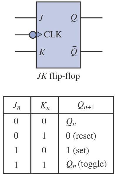
32 JK flip-flop Same as RS FF except that J = K = states J Q CLK K Q J K Q No change Reset Set Toggle J Q CLK K Q J K CLK Q 32

33 indicating trailing edge-triggerc (no change) 33
34 J K Q 34
35 Master/slave FF Delayed output by the width of clock pulse Master Slave J K Q n+ J Q CLK K Q J Q CLK K Q Q n (no change) Reset Set Q n (toggle) CLK J t n master t n+ slave K Q 35
36 T flip-flop JK FF with its inputs tied together 36
37 클럭이들어올때마다상태가바뀌는회로 출력신호가정확히 T 입력신호주파수의절반 + V CC Q D Q J Q T T CLK Q T CLK Q K Q D FF JK FF T Q EN J Q EN T CLK K Q Q 37
38 3-bit binary up counter Force a RESET 38

39 Decade counter Count from to 9 and then RESET Impractical due to propagation delays 39
40 Ripple counter Consists of a cascade of 3 JK FFs 4
41 Ripple-up counter Asynchronous counter T FF n serial cascades = (2 n ) counter Slow CLK Q (LSB) Q Q 2 Q Q T Q T Q 2 T 2 Q Q Q Q Q 2 Q T Q T Q 2 T 2 Q Q 4
42 Ripple-down counter Asynchronous counter CLK Q (LSB) Q Q 2 Q Q T Q T Q 2 T 2 Q Q
43 Synchronous counter Parallel counter Fast Complex Q Q Q 2 Q 3 J Q J Q J 2 Q 2 J 3 Q 3 CLK CLK CLK CLK K K K 2 K 3 F F F 2 F 3 + V CC 43
44

45 Divider circuit 45
46 Synchronous counter 46

47 Ring counter 47

48 Parallel register The load input (clock) simultaneously transfers the parallel input binary word b 3 b 2 b b (store!) 48

49 Shift register 49
LOGIC CIRCUITS. Basic Experiment and Design of Electronics
 Basic Experiment and Design of Electronics LOGIC CIRCUITS Ho Kyung Kim, Ph.D. hokyung@pusan.ac.kr School of Mechanical Engineering Pusan National University Outline Combinational logic circuits Output
Sample Test Paper - I
 Scheme G Sample Test Paper - I Course Name : Computer Engineering Group Marks : 25 Hours: 1 Hrs. Q.1) Attempt any THREE: 09 Marks a) Define i) Propagation delay ii) Fan-in iii) Fan-out b) Convert the following:
 vidyarthiplus.com vidyarthiplus.com vidyarthiplus.com ANNA UNIVERSITY- COMBATORE B.E./ B.TECH. DEGREE EXAMINATION - JUNE 2009. ELECTRICAL & ELECTONICS ENGG. - FOURTH SEMESTER DIGITAL LOGIC CIRCUITS PART-A
Reg. No. Question Paper Code : B.E./B.Tech. DEGREE EXAMINATION, NOVEMBER/DECEMBER Second Semester. Computer Science and Engineering
 Sp 6 Reg. No. Question Paper Code : 27156 B.E./B.Tech. DEGREE EXAMINATION, NOVEMBER/DECEMBER 2015. Second Semester Computer Science and Engineering CS 6201 DIGITAL PRINCIPLES AND SYSTEM DESIGN (Common
S.Y. Diploma : Sem. III [DE/ED/EI/EJ/EN/ET/EV/EX/IC/IE/IS/IU/MU] Principles of Digital Techniques
![S.Y. Diploma : Sem. III [DE/ED/EI/EJ/EN/ET/EV/EX/IC/IE/IS/IU/MU] Principles of Digital Techniques](/thumbs/82/86792063.jpg "S.Y. Diploma : Sem. III [DE/ED/EI/EJ/EN/ET/EV/EX/IC/IE/IS/IU/MU] Principles of Digital Techniques") S.Y. Diploma : Sem. III [DE/ED/EI/EJ/EN/ET/EV/EX/IC/IE/IS/IU/MU] Principles of Digital Techniques Time: 3 Hrs.] Prelim Question Paper Solution [Marks : 100 Q.1(a) Attempt any SIX of the following : [12]
S.Y. Diploma : Sem. III [DE/ED/EI/EJ/EN/ET/EV/EX/IC/IE/IS/IU/MU] Principles of Digital Techniques Time: 3 Hrs.] Prelim Question Paper Solution [Marks : 100 Q.1(a) Attempt any SIX of the following : [12]
DIGITAL LOGIC CIRCUITS
 DIGITAL LOGIC CIRCUITS Introduction Logic Gates Boolean Algebra Map Specification Combinational Circuits Flip-Flops Sequential Circuits Memory Components Integrated Circuits Digital Computers 2 LOGIC GATES
MAHARASHTRA STATE BOARD OF TECHNICAL EDUCATION (Autonomous) (ISO/IEC Certified) State any two Boolean laws. (Any 2 laws 1 mark each)
 (ISO/IEC Certified) State any two Boolean laws. (Any 2 laws 1 mark each)") Subject Code: 17333 Model Answer Page 1/ 27 Important Instructions to examiners: 1) The answers should be examined by key words and not as word-to-word as given in the model answer scheme. 2) The model
Subject Code: 17333 Model Answer Page 1/ 27 Important Instructions to examiners: 1) The answers should be examined by key words and not as word-to-word as given in the model answer scheme. 2) The model
MAHARASHTRA STATE BOARD OF TECHNICAL EDUCATION (Autonomous) (ISO/IEC Certified)
 (ISO/IEC Certified)") WINTER 17 EXAMINATION Subject Name: Digital Techniques Model Answer Subject Code: 17333 Important Instructions to examiners: 1) The answers should be examined by key words and not as word-to-word as given
WINTER 17 EXAMINATION Subject Name: Digital Techniques Model Answer Subject Code: 17333 Important Instructions to examiners: 1) The answers should be examined by key words and not as word-to-word as given
on candidate s understanding. 7) For programming language papers, credit may be given to any other program based on equivalent concept.
 For programming language papers, credit may be given to any other program based on equivalent concept.") WINTER 17 EXAMINATION Subject Name: Digital Techniques Model Answer Subject Code: 17333 Important Instructions to examiners: 1) The answers should be examined by key words and not as word-to-word as given
WINTER 17 EXAMINATION Subject Name: Digital Techniques Model Answer Subject Code: 17333 Important Instructions to examiners: 1) The answers should be examined by key words and not as word-to-word as given
Digital Electronics Circuits 2017
 JSS SCIENCE AND TECHNOLOGY UNIVERSITY Digital Electronics Circuits (EC37L) Lab in-charge: Dr. Shankraiah Course outcomes: After the completion of laboratory the student will be able to, 1. Simplify, design
DE58/DC58 LOGIC DESIGN DEC 2014
 Q.2 a. In a base-5 number system, 3 digit representations is used. Find out (i) Number of distinct quantities that can be represented.(ii) Representation of highest decimal number in base-5. Since, r=5
SIR C.R.REDDY COLLEGE OF ENGINEERING ELURU DIGITAL INTEGRATED CIRCUITS (DIC) LABORATORY MANUAL III / IV B.E. (ECE) : I - SEMESTER
 LABORATORY MANUAL III / IV B.E. (ECE) : I - SEMESTER") SIR C.R.REDDY COLLEGE OF ENGINEERING ELURU 534 007 DIGITAL INTEGRATED CIRCUITS (DIC) LABORATORY MANUAL III / IV B.E. (ECE) : I - SEMESTER DEPARTMENT OF ELECTRONICS AND COMMUNICATION ENGINEERING DIGITAL
SIR C.R.REDDY COLLEGE OF ENGINEERING ELURU 534 007 DIGITAL INTEGRATED CIRCUITS (DIC) LABORATORY MANUAL III / IV B.E. (ECE) : I - SEMESTER DEPARTMENT OF ELECTRONICS AND COMMUNICATION ENGINEERING DIGITAL
CHW 261: Logic Design
 CHW 26: Logic Design Instructors: Prof. Hala Zayed Dr. Ahmed Shalaby http://www.bu.edu.eg/staff/halazayed4 http://bu.edu.eg/staff/ahmedshalaby4# Slide Digital Fundamentals CHAPTER 8 Counters Slide 2 Counting
Digital Circuits ECS 371
 Digital Circuits ECS 371 Dr. Prapun Suksompong prapun@siit.tu.ac.th Lecture 18 Office Hours: BKD 3601-7 Monday 9:00-10:30, 1:30-3:30 Tuesday 10:30-11:30 1 Announcement Reading Assignment: Chapter 7: 7-1,
ELCT201: DIGITAL LOGIC DESIGN
 ELCT201: DIGITAL LOGIC DESIGN Dr. Eng. Haitham Omran, haitham.omran@guc.edu.eg Dr. Eng. Wassim Alexan, wassim.joseph@guc.edu.eg Lecture 6 Following the slides of Dr. Ahmed H. Madian محرم 1439 ه Winter
S.Y. Diploma : Sem. III [CO/CM/IF/CD/CW] Digital Techniques
![S.Y. Diploma : Sem. III [CO/CM/IF/CD/CW] Digital Techniques](/thumbs/90/103932933.jpg "S.Y. Diploma : Sem. III [CO/CM/IF/CD/CW] Digital Techniques") S.Y. Diploma : Sem. III [CO/CM/IF/CD/CW] Digital Techniques Time: 3 Hrs.] Prelim Question Paper Solution [Marks : 100 Q.1(a) Attempt any SIX of the following : [12] Q.1(a) (i) Derive AND gate and OR gate
S.Y. Diploma : Sem. III [CO/CM/IF/CD/CW] Digital Techniques Time: 3 Hrs.] Prelim Question Paper Solution [Marks : 100 Q.1(a) Attempt any SIX of the following : [12] Q.1(a) (i) Derive AND gate and OR gate
Lab 3 Revisited. Zener diodes IAP 2008 Lecture 4 1
 Lab 3 Revisited Zener diodes R C 6.091 IAP 2008 Lecture 4 1 Lab 3 Revisited +15 Voltage regulators 555 timers 270 1N758 0.1uf 5K pot V+ V- 2N2222 0.1uf V o. V CC V Vin s = 5 V Vc V c Vs 1 e t = RC Threshold
Vidyalankar S.E. Sem. III [CMPN] Digital Logic Design and Analysis Prelim Question Paper Solution
![Vidyalankar S.E. Sem. III [CMPN] Digital Logic Design and Analysis Prelim Question Paper Solution](/thumbs/90/103673562.jpg "Vidyalankar S.E. Sem. III [CMPN] Digital Logic Design and Analysis Prelim Question Paper Solution") . (a) (i) ( B C 5) H (A 2 B D) H S.E. Sem. III [CMPN] Digital Logic Design and Analysis Prelim Question Paper Solution ( B C 5) H (A 2 B D) H = (FFFF 698) H (ii) (2.3) 4 + (22.3) 4 2 2. 3 2. 3 2 3. 2 (2.3)
. (a) (i) ( B C 5) H (A 2 B D) H S.E. Sem. III [CMPN] Digital Logic Design and Analysis Prelim Question Paper Solution ( B C 5) H (A 2 B D) H = (FFFF 698) H (ii) (2.3) 4 + (22.3) 4 2 2. 3 2. 3 2 3. 2 (2.3)
CHW 261: Logic Design
 CHW 26: Logic Design Instructors: Prof. Hala Zayed Dr. Ahmed Shalaby http://www.bu.edu.eg/staff/halazayed4 http://bu.edu.eg/staff/ahmedshalaby4# Slide Digital Fundamentals Digital Concepts Slide 2 What?
Layout of 7400-series Chips Commonly Used in. CDA 3101: Introduction to Computer Hardware and Organization
 Layout of 400-series Chips Commonly Used in CDA 30: Introduction to Computer Hardware and Organization Charles N. Winton Department of Computer and Information Sciences University of North Florida 999
DHANALAKSHMI COLLEGE OF ENGINEERING, CHENNAI DEPARTMENT OF COMPUTER SCIENCE AND ENGINEERING CS6201 DIGITAL PRINCIPLES AND SYSTEM DESIGN
 DHANALAKSHMI COLLEGE OF ENGINEERING, CHENNAI DEPARTMENT OF COMPUTER SCIENCE AND ENGINEERING CS6201 DIGITAL PRINCIPLES AND SYSTEM DESIGN UNIT I : BOOLEAN ALGEBRA AND LOGIC GATES PART - A (2 MARKS) Number
Sequential vs. Combinational
 Sequential Circuits Sequential vs. Combinational Combinational Logic: Output depends only on current input TV channel selector (-9) inputs system outputs Sequential Logic: Output depends not only on current
ECE 341. Lecture # 3
 ECE 341 Lecture # 3 Instructor: Zeshan Chishti zeshan@ece.pdx.edu October 7, 2013 Portland State University Lecture Topics Counters Finite State Machines Decoders Multiplexers Reference: Appendix A of
Introduction to Computer Engineering. CS/ECE 252, Fall 2012 Prof. Guri Sohi Computer Sciences Department University of Wisconsin Madison
 Introduction to Computer Engineering CS/ECE 252, Fall 2012 Prof. Guri Sohi Computer Sciences Department University of Wisconsin Madison Chapter 3 Digital Logic Structures Slides based on set prepared by
SUMMER 18 EXAMINATION Subject Name: Principles of Digital Techniques Model Answer Subject Code:
 Important Instructions to examiners: 1) The answers should be examined by key words and not as word-to-word as given in the model answer scheme. 2) The model answer and the answer written by candidate
Vidyalankar S.E. Sem. III [EXTC] Digital Electronics Prelim Question Paper Solution ABCD ABCD ABCD ABCD ABCD ABCD ABCD ABCD = B
![Vidyalankar S.E. Sem. III [EXTC] Digital Electronics Prelim Question Paper Solution ABCD ABCD ABCD ABCD ABCD ABCD ABCD ABCD = B](/thumbs/84/91058397.jpg "Vidyalankar S.E. Sem. III [EXTC] Digital Electronics Prelim Question Paper Solution ABCD ABCD ABCD ABCD ABCD ABCD ABCD ABCD = B") . (a). (b). (c) S.E. Sem. III [EXTC] igital Electronics Prelim Question Paper Solution ABC ABC ABC ABC ABC ABC ABC ABC = B LHS = ABC ABC ABC ABC ABC ABC ABC ABC But ( ) = = ABC( ) ABC( ) ABC( ) ABC( )
. (a). (b). (c) S.E. Sem. III [EXTC] igital Electronics Prelim Question Paper Solution ABC ABC ABC ABC ABC ABC ABC ABC = B LHS = ABC ABC ABC ABC ABC ABC ABC ABC But ( ) = = ABC( ) ABC( ) ABC( ) ABC( )
PGT104 Digital Electronics. PGT104 Digital Electronics
 1 Part 6 Sequential Logic ircuits Disclaimer: Most of the contents (if not all) are extracted from resources available for Digital Fundamentals 10 th Edition 2 Basic Shift Register Operations A shift register
Chapter 7. Sequential Circuits Registers, Counters, RAM
 Chapter 7. Sequential Circuits Registers, Counters, RAM Register - a group of binary storage elements suitable for holding binary info A group of FFs constitutes a register Commonly used as temporary storage
Unit II Chapter 4:- Digital Logic Contents 4.1 Introduction... 4
 Unit II Chapter 4:- Digital Logic Contents 4.1 Introduction... 4 4.1.1 Signal... 4 4.1.2 Comparison of Analog and Digital Signal... 7 4.2 Number Systems... 7 4.2.1 Decimal Number System... 7 4.2.2 Binary
KUMARAGURU COLLEGE OF TECHNOLOGY COIMBATORE
 Estd-1984 KUMARAGURU COLLEGE OF TECHNOLOGY COIMBATORE 641 006 QUESTION BANK UNIT I PART A ISO 9001:2000 Certified 1. Convert (100001110.010) 2 to a decimal number. 2. Find the canonical SOP for the function
Digital Fundamentals
 Digital Fundamentals Tenth Edition Floyd Chapter 9 Sections 9-1 thru 9-5 2009 Pearson Education, Upper 2008 Pearson Saddle River, Education NJ 07458. All Rights Reserved ET285 Agenda Week 2 Quiz 0: Covered
Fundamentals of Boolean Algebra
 UNIT-II 1 Fundamentals of Boolean Algebra Basic Postulates Postulate 1 (Definition): A Boolean algebra is a closed algebraic system containing a set K of two or more elements and the two operators and
3 Logic Function Realization with MSI Circuits
 3 Logic Function Realization with MSI Circuits Half adder A half-adder is a combinational circuit with two binary inputs (augund and addend bits) and two binary outputs (sum and carry bits). It adds the
Sequential Logic. Rab Nawaz Khan Jadoon DCS. Lecturer COMSATS Lahore Pakistan. Department of Computer Science
 Sequential Logic Rab Nawaz Khan Jadoon DCS COMSATS Institute of Information Technology Lecturer COMSATS Lahore Pakistan Digital Logic and Computer Design Sequential Logic Combinational circuits with memory
I. Motivation & Examples
 I. Motivation & Examples Output depends on current input and past history of inputs. State embodies all the information about the past needed to predict current output based on current input. State variables,
Roger L. Tokheim. Chapter 8 Counters Glencoe/McGraw-Hill
 Digital Electronics Principles & Applications Sixth Edition Roger L. Tokheim Chapter 8 Counters 2003 Glencoe/McGraw-Hill INTRODUCTION Overview of Counters Characteristics of Counters Ripple Up Counter
ECE/Comp Sci 352 Digital Systems Fundamentals. Charles R. Kime Section 2 Fall Logic and Computer Design Fundamentals
 University of Wisconsin - Madison ECE/Comp Sci 352 Digital Systems Fundamentals Charles R. Kime Section 2 Fall 2001 Lecture 5 Registers & Counters Part 2 Charles Kime Counters Counters are sequential circuits
Digital Fundamentals
 Digital Fundamentals Tenth Edition Floyd hapter 8 Modified by Yuttapong Jiraraksopakun Floyd, Digital Fundamentals, 10 th 2008 Pearson Education ENE, KMUTT ed 2009 ounting in Binary As you know, the binary
Section 3: Combinational Logic Design. Department of Electrical Engineering, University of Waterloo. Combinational Logic
 Section 3: Combinational Logic Design Major Topics Design Procedure Multilevel circuits Design with XOR gates Adders and Subtractors Binary parallel adder Decoders Encoders Multiplexers Programmed Logic
MAHARASHTRA STATE BOARD OF TECHNICAL EDUCATION (Autonomous) (ISO/IEC Certified) SUMMER 14 EXAMINATION Model Answer
 (ISO/IEC Certified) SUMMER 14 EXAMINATION Model Answer") MAHARASHTRA STATE BOARD OF TECHNICAL EDUCATION (Autonomous) (ISO/IEC 27001 2005 Certified) SUMMER 14 EXAMINATION Model Answer Subject Code : 17320 Page No: 1/34 Important Instructions to examiners: 1)
MAHARASHTRA STATE BOARD OF TECHNICAL EDUCATION (Autonomous) (ISO/IEC 27001 2005 Certified) SUMMER 14 EXAMINATION Model Answer Subject Code : 17320 Page No: 1/34 Important Instructions to examiners: 1)
ECEN 248: INTRODUCTION TO DIGITAL SYSTEMS DESIGN. Week 9 Dr. Srinivas Shakkottai Dept. of Electrical and Computer Engineering
 ECEN 248: INTRODUCTION TO DIGITAL SYSTEMS DESIGN Week 9 Dr. Srinivas Shakkottai Dept. of Electrical and Computer Engineering TIMING ANALYSIS Overview Circuits do not respond instantaneously to input changes
King Fahd University of Petroleum and Minerals College of Computer Science and Engineering Computer Engineering Department
 King Fahd University of Petroleum and Minerals College of Computer Science and Engineering Computer Engineering Department Page 1 of 13 COE 202: Digital Logic Design (3-0-3) Term 112 (Spring 2012) Final
Unit 7 Sequential Circuits (Flip Flop, Registers)
") College of Computer and Information Sciences Department of Computer Science CSC 220: Computer Organization Unit 7 Sequential Circuits (Flip Flop, Registers) 2 SR Flip-Flop The SR flip-flop, also known
College of Computer and Information Sciences Department of Computer Science CSC 220: Computer Organization Unit 7 Sequential Circuits (Flip Flop, Registers) 2 SR Flip-Flop The SR flip-flop, also known
Memory, Latches, & Registers
 Memory, Latches, & Registers 1) Structured Logic Arrays 2) Memory Arrays 3) Transparent Latches 4) How to save a few bucks at toll booths 5) Edge-triggered Registers L13 Memory 1 General Table Lookup Synthesis
ELEC Digital Logic Circuits Fall 2014 Sequential Circuits (Chapter 6) Finite State Machines (Ch. 7-10)
 Finite State Machines (Ch. 7-10)") ELEC 2200-002 Digital Logic Circuits Fall 2014 Sequential Circuits (Chapter 6) Finite State Machines (Ch. 7-10) Vishwani D. Agrawal James J. Danaher Professor Department of Electrical and Computer Engineering
ELEC 2200-002 Digital Logic Circuits Fall 2014 Sequential Circuits (Chapter 6) Finite State Machines (Ch. 7-10) Vishwani D. Agrawal James J. Danaher Professor Department of Electrical and Computer Engineering
Appendix B. Review of Digital Logic. Baback Izadi Division of Engineering Programs
 Appendix B Review of Digital Logic Baback Izadi Division of Engineering Programs bai@engr.newpaltz.edu Elect. & Comp. Eng. 2 DeMorgan Symbols NAND (A.B) = A +B NOR (A+B) = A.B AND A.B = A.B = (A +B ) OR
Lecture 7: Logic design. Combinational logic circuits
 /24/28 Lecture 7: Logic design Binary digital circuits: Two voltage levels: and (ground and supply voltage) Built from transistors used as on/off switches Analog circuits not very suitable for generic
Vidyalankar S.E. Sem. III [ETRX] Digital Circuits and Design Prelim Question Paper Solution
![Vidyalankar S.E. Sem. III [ETRX] Digital Circuits and Design Prelim Question Paper Solution](/thumbs/79/79145081.jpg "Vidyalankar S.E. Sem. III [ETRX] Digital Circuits and Design Prelim Question Paper Solution") S.E. Sem. III [ETRX] Digital Circuits and Design Prelim uestion Paper Solution. (a) Static Hazard Static hazards have two cases: static and static. static- hazard exists when the output variable should
S.E. Sem. III [ETRX] Digital Circuits and Design Prelim uestion Paper Solution. (a) Static Hazard Static hazards have two cases: static and static. static- hazard exists when the output variable should
Synchronous Sequential Logic
 1 IT 201 DIGITAL SYSTEMS DESIGN MODULE4 NOTES Synchronous Sequential Logic Sequential Circuits - A sequential circuit consists of a combinational circuit and a feedback through the storage elements in
Digital Logic: Boolean Algebra and Gates. Textbook Chapter 3
 Digital Logic: Boolean Algebra and Gates Textbook Chapter 3 Basic Logic Gates XOR CMPE12 Summer 2009 02-2 Truth Table The most basic representation of a logic function Lists the output for all possible
SAU1A FUNDAMENTALS OF DIGITAL COMPUTERS
 SAU1A FUNDAMENTALS OF DIGITAL COMPUTERS Unit : I - V Unit : I Overview Fundamentals of Computers Characteristics of Computers Computer Language Operating Systems Generation of Computers 2 Definition of
Department of Electrical & Electronics EE-333 DIGITAL SYSTEMS
 Department of Electrical & Electronics EE-333 DIGITAL SYSTEMS 1) Given the two binary numbers X = 1010100 and Y = 1000011, perform the subtraction (a) X -Y and (b) Y - X using 2's complements. a) X = 1010100
University of Toronto Faculty of Applied Science and Engineering Edward S. Rogers Sr. Department of Electrical and Computer Engineering
 University of Toronto Faculty of Applied Science and Engineering Edward S. Rogers Sr. Department of Electrical and Computer Engineering Final Examination ECE 241F - Digital Systems Examiners: J. Rose and
ELCT201: DIGITAL LOGIC DESIGN
 ELCT201: DIGITAL LOGIC DESIGN Dr. Eng. Haitham Omran, haitham.omran@guc.edu.eg Dr. Eng. Wassim Alexan, wassim.joseph@guc.edu.eg Following the slides of Dr. Ahmed H. Madian Lecture 10 محرم 1439 ه Winter
Ch 9. Sequential Logic Technologies. IX - Sequential Logic Technology Contemporary Logic Design 1
 Ch 9. Sequential Logic Technologies Technology Contemporary Logic Design Overview Basic Sequential Logic Components FSM Design with Counters FSM Design with Programmable Logic FSM Design with More Sophisticated
CMPE12 - Notes chapter 1. Digital Logic. (Textbook Chapter 3)
") CMPE12 - Notes chapter 1 Digital Logic (Textbook Chapter 3) Transistor: Building Block of Computers Microprocessors contain TONS of transistors Intel Montecito (2005): 1.72 billion Intel Pentium 4 (2000):
CMPE12 - Notes chapter 1 Digital Logic (Textbook Chapter 3) Transistor: Building Block of Computers Microprocessors contain TONS of transistors Intel Montecito (2005): 1.72 billion Intel Pentium 4 (2000):
INTEGRATED CIRCUITS. For a complete data sheet, please also download:
 INTEGRATED CIRCUITS DATA SHEET For a complete data sheet, please also download: The IC06 74HC/HCT/HCU/HCMOS Logic Family Specifications The IC06 74HC/HCT/HCU/HCMOS Logic Package Information The IC06 74HC/HCT/HCU/HCMOS
EECS150 - Digital Design Lecture 18 - Counters
 EECS150 - Digital Design Lecture 18 - Counters October 24, 2002 John Wawrzynek Fall 2002 EECS150 - Lec18-counters Page 1 Counters Special sequential circuits (FSMs) that sequence though a set outputs.
EECS150 - Digital Design Lecture 18 - Counters
 EECS50 - Digital Design Lecture 8 - Counters October 24, 2002 John Wawrzynek Fall 2002 EECS50 - Lec8-counters Page Counters Special sequential circuits (FSMs) that sequence though a set outputs. Examples:
EECS150 - Digital Design Lecture 11 - Shifters & Counters. Register Summary
 EECS50 - Digital Design Lecture - Shifters & Counters February 24, 2003 John Wawrzynek Spring 2005 EECS50 - Lec-counters Page Register Summary All registers (this semester) based on Flip-flops: q 3 q 2
L4: Sequential Building Blocks (Flip-flops, Latches and Registers)
") L4: Sequential Building Blocks (Flip-flops, Latches and Registers) Acknowledgements: Lecture material adapted from R. Katz, G. Borriello, Contemporary Logic esign (second edition), Prentice-Hall/Pearson
L4: Sequential Building Blocks (Flip-flops, Latches and Registers) Acknowledgements: Lecture material adapted from R. Katz, G. Borriello, Contemporary Logic esign (second edition), Prentice-Hall/Pearson
MAHALAKSHMI ENGINEERING COLLEGE TIRUCHIRAPALLI
 DEPARTMENT: ECE MAHALAKSHMI ENGINEERING COLLEGE TIRUCHIRAPALLI 6 QUESTION BANK SUBJECT NAME: DIGITAL ELECTRONICS UNIT : Design of Sequential Circuits PART A ( Marks). Draw the logic diagram 4: Multiplexer.(AUC
ESE 570: Digital Integrated Circuits and VLSI Fundamentals
 ESE 570: Digital Integrated Circuits and VLSI Fundamentals Lec 17: March 23, 2017 Energy and Power Optimization, Design Space Exploration, Synchronous MOS Logic Lecture Outline! Energy and Power Optimization
Topics. Dynamic CMOS Sequential Design Memory and Control. John A. Chandy Dept. of Electrical and Computer Engineering University of Connecticut
 Topics Dynamic CMOS Sequential Design Memory and Control Dynamic CMOS In static circuits at every point in time (except when switching) the output is connected to either GND or V DD via a low resistance
Dept. of ECE, CIT, Gubbi Page 1
 Verification: 1) A.B = A + B 7404 7404 7404 A B A.B A.B 0 0 0 1 0 1 0 1 1 0 0 1 1 1 1 0 A B A B A + B 0 0 1 1 1 0 1 1 0 1 1 0 0 1 1 1 1 0 0 0 2) A+B = A. B 7404 7404 7404 A B A+B A+B 0 0 0 1 0 1 1 0 1
Digital Logic Appendix A
 Digital Logic Appendix A Boolean Algebra Gates Combinatorial Circuits Sequential Circuits 1 Boolean Algebra George Boole ideas 1854 Claude Shannon, apply to circuit design, 1938 Describe digital circuitry
Shift Register Counters
 Shift Register Counters Shift register counter: a shift register with the serial output connected back to the serial input. They are classified as counters because they give a specified sequence of states.
Introduction EE 224: INTRODUCTION TO DIGITAL CIRCUITS & COMPUTER DESIGN. Lecture 6: Sequential Logic 3 Registers & Counters 5/9/2010
 EE 224: INTROUCTION TO IGITAL CIRCUITS & COMPUTER ESIGN Lecture 6: Sequential Logic 3 Registers & Counters 05/10/2010 Avinash Kodi, kodi@ohio.edu Introduction 2 A Flip-Flop stores one bit of information
Introduction to Computer Engineering. CS/ECE 252, Spring 2017 Rahul Nayar Computer Sciences Department University of Wisconsin Madison
 Introduction to Computer Engineering CS/ECE 252, Spring 2017 Rahul Nayar Computer Sciences Department University of Wisconsin Madison Chapter 3 Digital Logic Structures Slides based on set prepared by
Lecture 9: Digital Electronics
 Introduction: We can classify the building blocks of a circuit or system as being either analog or digital in nature. If we focus on voltage as the circuit parameter of interest: nalog: The voltage can
Chapter 7 Sequential Logic
 Chapter 7 Sequential Logic SKEE2263 Digital Systems Mun im/ismahani/izam {munim@utm.my,e-izam@utm.my,ismahani@fke.utm.my} March 28, 2016 Table of Contents 1 Intro 2 Bistable Circuits 3 FF Characteristics
ALU A functional unit
 ALU A functional unit that performs arithmetic operations such as ADD, SUB, MPY logical operations such as AND, OR, XOR, NOT on given data types: 8-,16-,32-, or 64-bit values A n-1 A n-2... A 1 A 0 B n-1
Gates and Flip-Flops
 Gates and Flip-Flops Chris Kervick (11355511) With Evan Sheridan and Tom Power December 2012 On a scale of 1 to 10, how likely is it that this question is using binary?...4? What s a 4? Abstract The operation
NTE74176 Integrated Circuit TTL 35Mhz Presettable Decade Counter/Latch
 NTE74176 Integrated Circuit TTL 35Mhz Presettable Decade Counter/Latch Description: The NTE74176 is a high speed monolithic counter in a 14 Lead plastic DIP type package consisting of four DC coupled master
EECS150 - Digital Design Lecture 17 - Sequential Circuits 3 (Counters)
") EECS150 - Digital Design Lecture 17 - Sequential Circuits 3 (Counters) March 19&21, 2002 John Wawrzynek Spring 2002 EECS150 - Lec13-seq3 version 2 Page 1 Counters Special sequential circuits (FSMs) that
EECS150 - Digital Design Lecture 17 - Sequential Circuits 3 (Counters) March 19&21, 2002 John Wawrzynek Spring 2002 EECS150 - Lec13-seq3 version 2 Page 1 Counters Special sequential circuits (FSMs) that
Sequential Logic Circuits
 Chapter 4 Sequential Logic Circuits 4 1 The defining characteristic of a combinational circuit is that its output depends only on the current inputs applied to the circuit. The output of a sequential circuit,
MAHALAKSHMI ENGINEERING COLLEGE TIRUCHIRAPALLI
 MAHALAKSHMI ENGINEERING COLLEGE TIRUCHIRAPALLI 6 DEPARTMENT: EEE QUESTION BANK SUBJECT NAME: DIGITAL LOGIC CIRCUITS SUBJECT CODE: EE55 SEMESTER IV UNIT : Design of Synchronous Sequential Circuits PART
Fundamentals of Digital Design
 Fundamentals of Digital Design Digital Radiation Measurement and Spectroscopy NE/RHP 537 1 Binary Number System The binary numeral system, or base-2 number system, is a numeral system that represents numeric
Experiment 9 Sequential Circuits
 Introduction to Counters Experiment 9 Sequential Circuits The aim of this experiment is to familiarize you, frst with the basic sequential circuit device called a fip fop, and then, with the design and
Digital Electronics Final Examination. Part A
 Digital Electronics Final Examination Part A Spring 2009 Student Name: Date: Class Period: Total Points: /50 Converted Score: /40 Page 1 of 13 Directions: This is a CLOSED BOOK/CLOSED NOTES exam. Select
Design of Sequential Circuits
 Design of Sequential Circuits Seven Steps: Construct a state diagram (showing contents of flip flop and inputs with next state) Assign letter variables to each flip flop and each input and output variable
Lecture Outline. ESE 570: Digital Integrated Circuits and VLSI Fundamentals. Total Power. Energy and Power Optimization. Worksheet Problem 1
 ESE 570: Digital Integrated Circuits and VLSI Fundamentals Lec 16: March 20, 2018 Energy and Power Optimization, Design Space Exploration Lecture Outline! Energy and Power Optimization " Tradeoffs! Design
MODEL ANSWER SUMMER 17 EXAMINATION Subject Title: Principles of Digital Techniques
 MODEL ANSWER SUMMER 17 EXAMINATION Subject Title: Principles of Digital Techniques Subject Code: Important Instructions to examiners: 1) The answers should be examined by key words and not as word-to-word
COE 202: Digital Logic Design Sequential Circuits Part 4. Dr. Ahmad Almulhem ahmadsm AT kfupm Phone: Office:
 COE 202: Digital Logic Design Sequential Circuits Part 4 Dr. Ahmad Almulhem Email: ahmadsm AT kfupm Phone: 860-7554 Office: 22-324 Objectives Registers Counters Registers 0 1 n-1 A register is a group
NTE74177 Integrated Circuit TTL 35Mhz Presettable Binary Counter/Latch
 NTE74177 Integrated Circuit TTL 35Mhz Presettable Binary Counter/Latch Description: The NTE74177 is a high speed monolithic counter in a 14 Lead plastic DIP type package consisting of four DC coupled master
MOSIS REPORT. Spring MOSIS Report 1. MOSIS Report 2. MOSIS Report 3
 MOSIS REPORT Spring 2010 MOSIS Report 1 MOSIS Report 2 MOSIS Report 3 MOSIS Report 1 Design of 4-bit counter using J-K flip flop I. Objective The purpose of this project is to design one 4-bit counter
Boolean Algebra. Digital Logic Appendix A. Postulates, Identities in Boolean Algebra How can I manipulate expressions?
 Digital Logic Appendix A Gates Combinatorial Circuits Sequential Circuits Other operations NAND A NAND B = NOT ( A ANDB) = AB NOR A NOR B = NOT ( A ORB) = A + B Truth tables What is the result of the operation
Digital Electronic Meters
 Digital Electronic Meters EIE 240 Electrical and Electronic Measurement May 1, 2015 1 Digital Signal Binary or two stages: 0 (Low voltage 0-3 V) 1 (High voltage 4-5 V) Binary digit is called bit. Group
Vidyalankar. S.E. Sem. III [EXTC] Digital System Design. Q.1 Solve following : [20] Q.1(a) Explain the following decimals in gray code form
![Vidyalankar. S.E. Sem. III [EXTC] Digital System Design. Q.1 Solve following : [20] Q.1(a) Explain the following decimals in gray code form](/thumbs/96/126594189.jpg "Vidyalankar. S.E. Sem. III [EXTC] Digital System Design. Q.1 Solve following : [20] Q.1(a) Explain the following decimals in gray code form") S.E. Sem. III [EXTC] Digital System Design Time : 3 Hrs.] Prelim Paper Solution [Marks : 80 Q.1 Solve following : [20] Q.1(a) Explain the following decimals in gray code form [5] (i) (42) 10 (ii) (17)
S.E. Sem. III [EXTC] Digital System Design Time : 3 Hrs.] Prelim Paper Solution [Marks : 80 Q.1 Solve following : [20] Q.1(a) Explain the following decimals in gray code form [5] (i) (42) 10 (ii) (17)
ELECTRONICS & COMMUNICATION ENGINEERING PROFESSIONAL ETHICS AND HUMAN VALUES
 EC 216(R-15) Total No. of Questions :09] [Total No. of Pages : 02 II/IV B.Tech. DEGREE EXAMINATIONS, DECEMBER- 2016 First Semester ELECTRONICS & COMMUNICATION ENGINEERING PROFESSIONAL ETHICS AND HUMAN
ELEN Electronique numérique
 ELEN0040 - Electronique numérique Patricia ROUSSEAUX Année académique 2014-2015 CHAPITRE 3 Combinational Logic Circuits ELEN0040 3-4 1 Combinational Functional Blocks 1.1 Rudimentary Functions 1.2 Functions
INTEGRATED CIRCUITS. For a complete data sheet, please also download:
 INTEGRATED CIRCUITS DATA SHEET For a complete data sheet, please also download: The IC6 74HC/HCT/HCU/HCMOS ogic Family Specifications The IC6 74HC/HCT/HCU/HCMOS ogic Package Information The IC6 74HC/HCT/HCU/HCMOS
NOTE: The Flatpak version has the same pinouts (Connection Diagram) as the Dual In-Line Package. *MR for LS160A and LS161A *SR for LS162A and LS163A
 as the Dual In-Line Package. *MR for LS160A and LS161A *SR for LS162A and LS163A") BCD DECADE COUNTERS/ 4-BIT BINARY COUNTERS The LS160A/ 161A/ 162A/ 163A are high-speed 4-bit synchronous counters. They are edge-triggered, synchronously presettable, and cascadable MSI building blocks
BCD DECADE COUNTERS/ 4-BIT BINARY COUNTERS The LS160A/ 161A/ 162A/ 163A are high-speed 4-bit synchronous counters. They are edge-triggered, synchronously presettable, and cascadable MSI building blocks
Topic 8: Sequential Circuits
 Topic 8: Sequential Circuits Readings : Patterson & Hennesy, Appendix B.4 - B.6 Goals Basic Principles behind Memory Elements Clocks Applications of sequential circuits Introduction to the concept of the
Computers also need devices capable of Storing data and information Performing mathematical operations on such data
 Sequential Machines Introduction Logic devices examined so far Combinational Output function of input only Output valid as long as input true Change input change output Computers also need devices capable
Digital Logic. CS211 Computer Architecture. l Topics. l Transistors (Design & Types) l Logic Gates. l Combinational Circuits.
 l Logic Gates. l Combinational Circuits.") CS211 Computer Architecture Digital Logic l Topics l Transistors (Design & Types) l Logic Gates l Combinational Circuits l K-Maps Figures & Tables borrowed from:! http://www.allaboutcircuits.com/vol_4/index.html!
CS211 Computer Architecture Digital Logic l Topics l Transistors (Design & Types) l Logic Gates l Combinational Circuits l K-Maps Figures & Tables borrowed from:! http://www.allaboutcircuits.com/vol_4/index.html!
INTEGRATED CIRCUITS. For a complete data sheet, please also download:
 INTEGRATED CIRCUITS DATA SEET For a complete data sheet, please also download: The IC0 74C/CT/CU/CMOS ogic Family Specifications The IC0 74C/CT/CU/CMOS ogic Package Information The IC0 74C/CT/CU/CMOS ogic
( c) Give logic symbol, Truth table and circuit diagram for a clocked SR flip-flop. A combinational circuit is defined by the function
 Give logic symbol, Truth table and circuit diagram for a clocked SR flip-flop. A combinational circuit is defined by the function") Question Paper Digital Electronics (EE-204-F) MDU Examination May 2015 1. (a) represent (32)10 in (i) BCD 8421 code (ii) Excess-3 code (iii) ASCII code (b) Design half adder using only NAND gates. ( c)
Question Paper Digital Electronics (EE-204-F) MDU Examination May 2015 1. (a) represent (32)10 in (i) BCD 8421 code (ii) Excess-3 code (iii) ASCII code (b) Design half adder using only NAND gates. ( c)
Lecture 3 Review on Digital Logic (Part 2)
") Lecture 3 Review on Digital Logic (Part 2) Xuan Silvia Zhang Washington University in St. Louis http://classes.engineering.wustl.edu/ese461/ ircuit Optimization Simplest implementation ost criterion literal
Lecture 3 Review on Digital Logic (Part 2) Xuan Silvia Zhang Washington University in St. Louis http://classes.engineering.wustl.edu/ese461/ ircuit Optimization Simplest implementation ost criterion literal
(Boolean Algebra, combinational circuits) (Binary Codes and -arithmetics)
 (Binary Codes and -arithmetics)") Task 1. Exercises: Logical Design of Digital Systems Seite: 1 Self Study (Boolean Algebra, combinational circuits) 1.1 Minimize the function f 1 a ab ab by the help of Boolean algebra and give an implementation
Task 1. Exercises: Logical Design of Digital Systems Seite: 1 Self Study (Boolean Algebra, combinational circuits) 1.1 Minimize the function f 1 a ab ab by the help of Boolean algebra and give an implementation