Fundamentals of Boolean Algebra
|
|
|
- Abigayle Fowler
- 5 years ago
- Views:
Transcription
1 UNIT-II 1
2 Fundamentals of Boolean Algebra Basic Postulates Postulate 1 (Definition): A Boolean algebra is a closed algebraic system containing a set K of two or more elements and the two operators and +. Postulate 2 (Existence of 1 and 0 element): (a) a + 0 = a (identity for +), (b) a 1 = a (identity for ) Postulate 3 (Commutativity): (a) a + b = b + a, (b) a b = b a Postulate 4 (Associativity): (a) a + (b + c) = (a + b) + c Postulate 5 (Distributivity): (a) a + (b c) = (a + b) (a + c) (b) a (b c) = (a b) c (b) a (b + c) = a b + a c Postulate 6 (Existence of complement): (a) A 1 (b) A Normally is omitted. A 0 A 2
3 Fundamentals of Boolean Algebra Fundamental Theorems of Boolean Algebra Theorem 1 (Idempotency): (a) a + a = a Theorem 2 (Null element): (b) aa = a (a) a + 1 = 1 (b) a0 = 0 Theorem 3 (Involution) A A Properties of 0 and 1 elements (Table 2.1): OR AND Complement a + 0 = 0 a0 = 0 0' = 1 a + 1 = 1 a1 = a 1' = 0 3
4 Fundamentals of Boolean Algebra (3) Theorem 4 (Absorption) (a) a + ab = a Examples: (X + Y) + (X + Y)Z = X + Y AB'(AB' + B'C) = AB' Theorem 5 (a) a + a'b = a + b (b) a(a + b) = a (b) a(a' + b) = ab Examples: B + AB'C'D = B + AC'D (X + Y)((X + Y)' + Z) = (X + Y)Z 4
5 Fundamentals of Boolean Algebra (4) Theorem 6 (a) ab + ab' = a (b) (a + b)(a + b') = a Examples: ABC + AB'C = AC (W' + X' + Y' + Z')(W' + X' + Y' + Z)(W' + X' + Y + Z')(W' + X' + Y + Z) = (W' + X' + Y')(W' + X' + Y + Z')(W' + X' + Y + Z) = (W' + X' + Y')(W' + X' + Y) = (W' + X') 5
6 Fundamentals of Boolean Algebra (5) Theorem 7 (a) ab + ab'c = ab + ac + c) = (a + b)(a + c) (b) (a + b)(a + b' Examples: wy' + wx'y + wxyz + wxz' = wy' + wx'y + wxy + wxz = wy' + wy + wxz' = w + wxz' = w (x'y' + z)(w + x'y' + z') = (x'y' + z)(w + x'y') 6
7 Fundamentals of Boolean Algebra (6) Theorem 8 (DeMorgan's Theorem) (a) (a + b)' = a'b' (b) (ab)' = a' + b' Generalized DeMorgan's Theorem (a) (a + b + z)' = a'b' z' Examples: (a + bc)' = (a + (bc))' = a'(bc)' = a'(b' + c') = a'b' + a'c' Note: (a + bc)' a'b' + c' (b) (ab z)' = a' + b' + z' 7
8 Logic Gates Electrical Signals and Logic Values Electric Signal Logic Value Positive Logic Negative Logic High Voltage (H) 1 0 Low Voltage (L) 0 1 A signal that is set to logic 1 is said to be asserted, active, or true. An active-high signal is asserted when it is high (positive logic). An active-low signal is asserted when it is low (negative logic). 8
9 AND Logic notation A B = C (Sometimes AB = C) A B C
10 OR Logic notation A + B = C A B C
11 A Q Inversion (NOT) Logic: Q A
12 Exclusive OR (XOR) Either A or B, but not both This is sometimes called the inequality detector, because the result will be 0 when the inputs are the same and 1 when they are different. The truth table is the same as for S on Binary Addition. S = A B A B S
13 UNIVERSAL GATES 13
14 NAND (NOT AND) Q A B A B Q
15 Basic Functional Components AND, OR, and NOT gates constructed exclusively from NAND gates A B AB F(A, B) = AB= AB A F(A, A) = AA = A AND gate NOT gate A A F(A, B) = A + B = A + B B B OR gate FNAND(A, A) A A A FNOT (A) FNAND(A, B) A B A B FAND(A, B) FNAND(A, B ) A B A B FOR (A, B) Hence, NAND gate may be used to implement all three elementary operators. 15
16 NOR (NOT OR) Q A B A B Q
17 Basic Functional Components AND, OR, and NOT gates constructed exclusively from NOR gates. A B A + B F(A, B) =A + B A F(A, A) =A + A = A OR gate NOT gate A A F(A, B) =AB= AB B B FNOR(A, A) A A A FNOT (A) AND gate FNOR(A, B) A B A B FOR (A, B) FNOR(A, B ) A B A B FAND(A, B) Hence, NOR gate may be used to implement all three elementary operators. 17
18 Summary Summary for all 2-input gates Inputs Output of each gate A B AND NAND OR NOR XOR XNOR
19 MINIMIZATON OF LOGIC EXPRESSION Goal -- minimize the cost of realizing a switching function Cost measures and other considerations Number of gates Number of levels Gate fan in and/or fan out Interconnection complexity Preventing hazards Two-level realizations Minimize the number of gates (terms in switching function) Minimize the fan in (literals in switching function) Commonly used techniques Boolean algebra postulates and theorems Karnaugh maps 19
20 Simplification Using Boolean Algebra A simplified Boolean expression uses the fewest gates possible to implement a given expression. A B C AB+A(B+C)+B(B+C) 20
 AB+AC+B+BC (B+BC=B) AB+AC+B (AB+B=B) B+AC A B C AB+A(B+C)+B(B+C) B A C")
21 Simplification Using Boolean Algebra AB+A(B+C)+B(B+C) (distributive law) AB+AB+AC+BB+BC (BB=B) AB+AB+AC+B+BC (AB+AB=AB) AB+AC+B+BC (B+BC=B) AB+AC+B (AB+B=B) B+AC A B C AB+A(B+C)+B(B+C) B A C B+AC 21
22 Simplification Using Boolean Algebra Try these: [ AB (C BD) A B ]C A BC AB C A B C AB C ABC AB AC A B C 22 8
23 Standard Forms of Boolean Expressions All Boolean expressions, regardless of their form, can be converted into either of two standard forms: The sum-of-products (SOP) form The product-of-sums (POS) form Standardization makes the evaluation, simplification, and implementation of Boolean expressions much more systematic and easier. 23

24 The Sum-of-Products (SOP) Form An SOP expression when two or more product terms are summed by Boolean addition. Examples: AB ABC ABC CDE B CD A B A BC AC Also: A A BC BCD In an SOP form, a single overbar cannot extend over more than one variable; however, more than one variable in a term can have an overbar: example: A B C is OK! BUT NOT: ABC 24
25 Converting Product Terms to Standard SOP Step 1: Multiply each nonstandard product term by a term made up of the sum of a missing variable and its complement. This results in two product terms. As you know, you can multiply anything by 1 without changing its value. Step 2: Repeat step 1 until all resulting product term contains all variables in the domain in either complemented or uncomplemented form. In converting a product term to standard form, the number of product terms is doubled for each missing variable. 25
26 Converting Product Terms to Standard SOP (example) Convert the following Boolean expression into standard SOP form: ABC AB ABC D AB C AB C (D D ) AB CD AB CD A B A B (C C ) A B C A B C A B C (D D ) A B C (D D ) A B CD A B CD A B C D A B C D AB C A B ABC D AB CD AB CD A B CD A B CD A B C D A B C D ABC D 26 8
27 The Product-of-Sums (POS) Form When two or more In a POS form, a single sum terms are overbar cannot extend multiplied, the result over more than one expression is a product- variable; however, more of-sums (POS): than one variable in a Examples: term can have an ( A B)( A B C ) overbar: ( A B C )(C D E)( B C D) example: A B C is OK! ( A B)( A B C )( A C ) BUT NOT: A B C Also: A( A B C)(B C D ) 27
28 Converting a Sum Term to Standard POS Step 1: Add to each nonstandard product term a term made up of the product of the missing variable and its complement. This results in two sum terms. As you know, you can add 0 to anything without changing its value. Step 2: Apply rule A+BC=(A+B)(A+C). Step 3: Repeat step 1 until all resulting sum terms contain all variable in the domain in either complemented or uncomplemented form. 28
29 Converting a Sum Term to Standard POS (example) Convert the following Boolean expression into standard POS form: ( A B C)(B C D )( A B C D) A B C A B C DD ( A B C D)( A B C D ) B C D B C D AA ( A B C D )( A B C D ) ( A B C )(B C D )( A B C D) ( A B C D)( A B C D )( A B C D )( A B C D )( A B C D) 29
30 Boolean Expressions & Truth Tables All standard Boolean expression can be easily converted into truth table format using binary values for each term in the expression. Also, standard SOP or POS expression can be determined from the truth table. 30
31 Converting SOP Expressions to Truth Table Format Recall the fact: An SOP expression is equal to 1 only if at least one of the product term is equal to 1. Constructing a truth table: Step 1: List all possible combinations of binary values of the variables in the expression. Step 2: Convert the SOP expression to standard form if it is not already. Step 3: Place a 1 in the output column (X) for each binary value that makes the standard SOP expression a 1 and place 0 for all the remaining binary values. 31

32 Converting SOP Expressions to Truth Table Format (example) Develop a truth table for the standard SOP expression ABC ABC ABC Inputs Output A B C X Product T erm A B C AB C ABC 32
33 Converting POS Expressions to Truth Table Format Recall the fact: A POS expression is equal to 0 only if at least one of the product term is equal to 0. Constructing a truth table: Step 1: List all possible combinations of binary values of the variables in the expression. Step 2: Convert the POS expression to standard form if it is not already. Step 3: Place a 0 in the output column (X) for each binary value that makes the standard POS expression a 0 and place 1 for all the remaining binary values. 33
 I nputs O utput Product A B C X Term 0 0 0 0 ( A B C) 0 0 1 1 ( A C) 0 1 0 0 B 0 1 1 0 ( A B C ) 1 0 0 1 1 0 1 0 ( A B C ) 1 1 0 0 ( A B C) 1 1 1 1 34")
34 Converting POS Expressions to Truth Table Format (example) Develop a truth table for the standard SOP expression ( A B C)( A B C)( A B C ) ( A B C )( A B C) I nputs O utput Product A B C X Term ( A B C) ( A C) B ( A B C ) ( A B C ) ( A B C)
35 Determining Standard Expression from a Truth Table To determine the standard SOP expression represented by a truth table. Instructions: Step 1: List the binary values of the input variables for which the output is 1. Step 2: Convert each binary value to the corresponding product term by replacing: each 1 with the corresponding variable, and each 0 with the corresponding variable complement. Example: 1010 AB CD 35
36 Determining Standard Expression from a Truth Table To determine the standard POS expression represented by a truth table. Instructions: Step 1: List the binary values of the input variables for which the output is 0. Step 2: Convert each binary value to the corresponding product term by replacing: each 1 with the corresponding variable complement, and each 0 with the corresponding variable. Example: 1001 A B C D 36
37 The Karnaugh Map Feel a little difficult using Boolean algebra laws, rules, and theorems to simplify logic? A K-map provides a systematic method for simplifying Boolean expressions and, if properly used, will produce the simplest SOP or POS expression possible, known as the minimum expression. 37
38 What is K-Map It s si ilar to truth ta le; i stead of ei g orga ized (i/p and o/p) into columns and rows, the K-map is an array of cells in which each cell represents a binary value of the input variables. The cells are arranged in a way so that simplification of a given expression is simply a matter of properly grouping the cells. K-maps can be used for expressions with 2, 3, 4, and 5 variables. 38


39 The 3 Variable K-Map There are 8 cells as shown: AB C A B C A B C 01 A BC A BC 11 ABC ABC 10 AB C AB C Or A A B C A B C A BC A BC 1 AB C AB C ABC ABC 39

40 The 4-Variable K-Map CD AB A B C D A B C D A B CDA B CD A BC D A BC D A BCD A BCD ABC D ABC D ABCD ABCD AB C D AB C D AB CD AB CD 40
41 K-Map SOP Minimization The K-Map is used for simplifying Boolean expressions to their minimal form. A minimized SOP expression contains the fewest possible terms with fewest possible variables per term. Generally, a minimum SOP expression can be implemented with fewer logic gates than a standard expression. 41
42 Karnaugh Maps (K-maps) If m i is a minterm of f, then place a 1 in cell i of the K-map. If M i is a maxterm of f, then place a 0 in cell i. If d i is a do t are of f, then place a d or x in cell i. 42
43 B 0 1 Examples Two variable K-map f(a,b)= m(0,1,3)=a`b`+a`b+ab A
44 Grouping the 1s (rules) 1. A group must contain either 1,2,4,8,or 16 cells (depending on number of variables in the expression) 2. Each cell in a group must be adjacent to one or more cells in that same group, but all cells in the group do not have to be adjacent to each other. 3. Always include the largest possible number of 1s in a group in accordance with rule Each 1 on the map must be included in at least one group. The 1s already in a group can be included in another group as long as the overlapping groups include noncommon 1s. 44
45 Determining the Minimum SOP Expression from the Map 2. Determine the minimum product term for each group. For a 3-variable map: 1. A 1-cell group yields a 3-variable product term 2. A 2-cell group yields a 2-variable product term 3. A 4-cell group yields a 1-variable product term 4. An 8-cell group yields a value of 1 for the expression. For a 4-variable map: 1. A 1-cell group yields a 4-variable product term 2. A 2-cell group yields a 3-variable product term 3. A 4-cell group yields a 2-variable product term 4. An 8-cell group yields a a 1-variable product term 5. A 16-cell group yields a value of 1 for the expression. 45

46 Determining the Minimum SOP Expression from the Map (example) AB CD B A C AC D A C B AC D 46
47 Three-Variable K-Maps f (0,4) B C f (4,5) A B f (0,1,4,5) B f (0,1,2,3) A BC BC BC BC A A A A f (0,4) A C f (4,6) A C f (0,2) A C f (0,2,4,6) C BC BC BC BC A A A A
48 Three-Variable K-Map Examples We can write any way either AB and C or A BC BC BC BC A A A BC BC BC A A A
 CD CD AB 00 01 11 10 AB")

49 Determining the Minimum SOP Expression from the Map (exercises) CD CD AB AB AB AC ABD D ABC BC 49
50 Four-Variable K-Maps CD CD CD CD AB AB AB AB f (4, 5, 6, 7) A B f (3, 7,11,15) C D f (0, 3, 5, 6, 9,10,12,15) f (1, 2, 4, 7, 8,11,13,14) f A B C D f A B C D CD CD CD CD AB AB AB AB f (1, 3,5, 7, 9,11,13,15) f (0,2,4,6,8,10,12,14) f (4,5,6,7,12,13,14,15) f (0,1,2,3,8,9,10,11) f D f D f B f B 50


51 Practicing K-Map (SOP) AB C A BC A B C A B C AB C B A C B C D A BC D ABC D A B CD AB CD A B CD A BCD ABCD AB CD D B C 51

52 0 1 Mapping Directly from a Truth Table I /P O /P A B C X AB C
53 Do t Care Co ditio s Sometimes a situation arises in which some input variable combinations are not allowed, i.e. BCD code: There are six invalid combinations: 1010, 1011, 1100, 1101, 1110, and Since these unallowed states will never occur in an application involving the BCD code they can be treated as do t are ter s ith respe t to their effect on the output. The do t are ter s a e used to ad a tage o the K- map (how? see the next slide). 53


54 Do t Care Co ditio s INPUTS O/P A B C D Y X X X X X X AB CD X Without do t are Y ABC ABCD 1 X X X 1 1 X X With do t are Y A BCD 54
55 Mapping a Standard POS Expression (full example) The expression: ( A B C)( A B C)( A B C)( A B C ) AB C
56 Combinational Circuits 56
57 57
58 Designing Combinational Circuits In general we have to do following steps: 1. Problem description 2. Input/output of the circuit 3. Define truth table 4. Simplification for each output 5. Draw the circuit 58
59 Decoder Is a combinational circuit that converts binary information from n input lines to a maximum of 2 n unique output lines For example if the number of input is n=3 the number of output lines can be m=2 3. It is also known as 1 of 8 because one output line is selected out of 8 available lines: 3 to 8 decoder enable 59
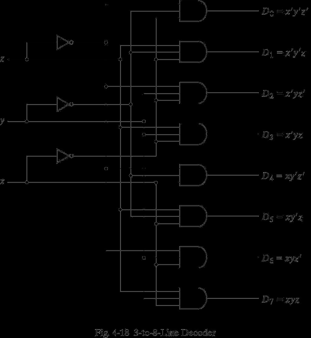
60 60
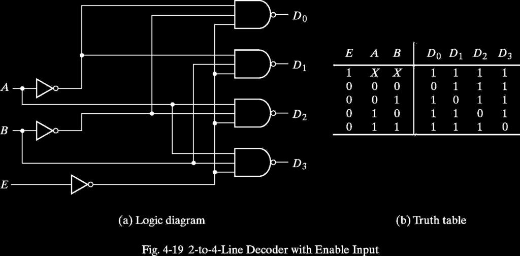
61 Decoder with Enable Line Decoders usually have an enable line, If enable=0, decoder is off. It means all output lines are zero If enable=1, decoder is on and depending on input, the corresponding output line is 1, all other lines are 0 See the truth table in next slide 61
62 Truth table for decoder E a2 a1 a0 D7 D6 D5 D4 D3 D2 D1 D x x x
63 63
64 Major application of Decoder Decoder is use to implement any combinational cicuits ( f n ) For e a ple the truth ta le for full adder is s,,z =,,, a d C,,z =,,,. The i ple e tatio ith de oder is: 64
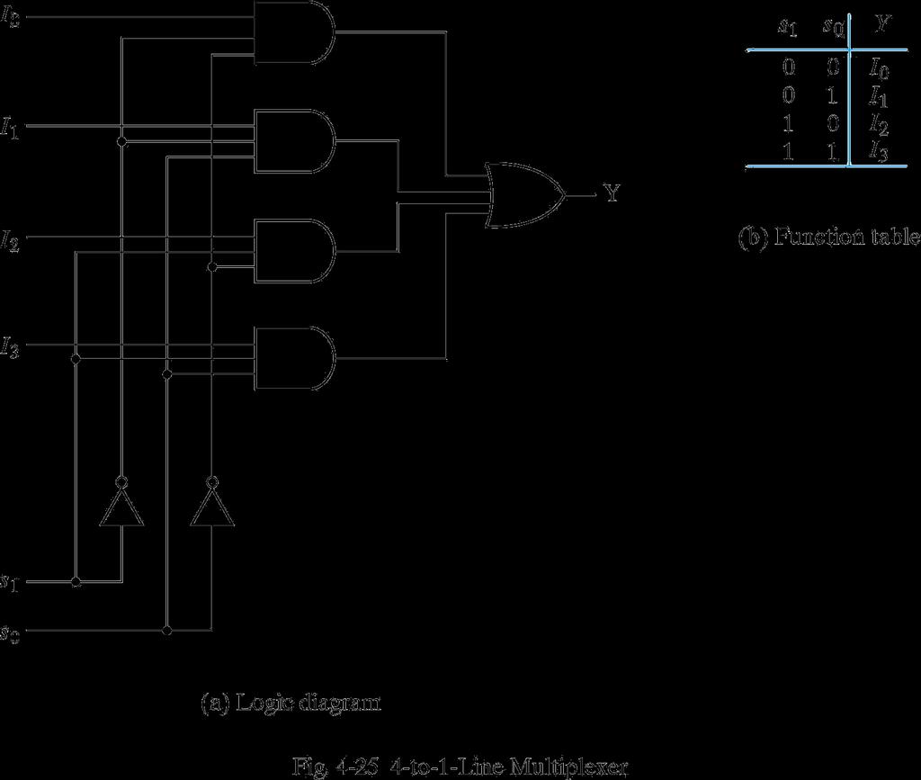
65 Multiplexer It is a combinational circuit that selects binary information from one of the input lines and directs it to a single output line Usually there are 2 n input lines and n selection lines whose bit combinations determine which input line is selected For example for 2-to-1 multiplexer if selection S is zero then I 0 has the path to output and if S is one I 1 has the path to output (see the next slide) 65
66 2-to-1 multiplexer 66
67 67
68 Boolean function Implementation Another method for implementing boolean function is using multiplexer For doing that assume boolean function has n variables. We have to use multiplexer with n- 1 selection lines and 1- first n-1 variables of function is used for data input 2- the remaining single variable ( named z )is used for data i put. Ea h data i put a e z, z, or. From truth table we have to find the relation of F and z to be able to design input lines. For example : f,,z =,,, 68
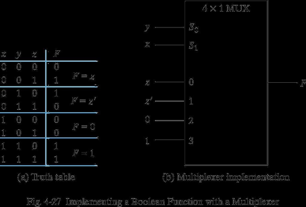
69 69
70 F A,B,C,D =,,,,,,, 70
71 Prgrammable Logic Organization Pre-fabricated building block of many AND/OR gates (or NOR, NAND) "Personalized" by making or breaking connections among the gates Inputs Dense array of Dense array of AND gates Product terms OR gates Outputs Programmable Array Block Diagram for Sum of Products Form 71
72 Basic Programmable Logic Organizations Depending on which of the AND/OR logic arrays is programmable, we have three basic organizations ORGANIZATION AND ARRAY OR ARRAY PAL PROG. FIXED PROM FIXED PROG. PLA PROG. PROG. 72
73 PLA Logic Implementation Key to Success: Shared Product Terms Example: Equations F0 = A + B C F1 = A C + A B F2 = B C + A B F3 = B C + A Personality Matrix Product Inputs Outputs term A B C F0 F 1 F 2 F 3 A B B C Reuse of A C terms B C A Input Side: 1 = asserted in term 0 = negated in term - = does not participate Output Side: 1 = term connected to output 0 = no connection to output 73
74 PLA Logic Implementation Example Continued - Unprogrammed device A B C All possible connections are available before programming F0 F1 F2 F3 74
75 Sequential Circuits Circuits require memory to store intermediate data Sequential circuits use a periodic signal to determine when to store values. A clock signal can determine storage times Clock signals are periodic Single bit storage element is a flip flop A basic type of flip flop is a latch Latches are made from logic gates NAND, NOR, AND, OR, Inverter 75
76 The story so far... Logical operations which respond to combinations of inputs to produce an output. Call these combinational logic circuits. For example, can add two numbers. But: No way of adding two numbers, then adding a third (a sequential operation); No way of remembering or storing information after inputs have been removed. To handle this, we need sequential logic capable of storing intermediate (and final) results. 76
77 Sequential Circuits Inputs Combinational circuit Next state Flip Flops Outputs Present state Timing signal (clock) Clock a periodic external event (input) synchronizes when current state changes happen keeps system well-behaved makes it easier to design and build large systems Clock 77
78 Sequential Circuits: Flip flops 78
79 Overview Latches respond to trigger levels on control inputs Example: If G = 1, input reflected at output Difficult to precisely time when to store data with latches Flip flips store data on a rising or falling trigger edge. Example: control input transitions from 0 -> 1, data input appears at output Data remains stable in the flip flop until until next rising edge. Different types of flip flops serve different functions Flip flops can be defined with characteristic functions. 79
80 D C S D Latch S Q R D C Q Q X 0 Q 0 Q 0 Q R S R C Q Q Q 0 Q 0 Store Reset Set Disallowed X X 0 Q 0 Q 0 Store When C is high, D passes from input to output (Q) 80
81 Master-Slave D Flip Flop Consider two latches combined together Only one C value active at a time Output changes on falling edge of the clock 81
82 D Flip-Flop Stores a value on the positive edge of C Input changes at other times have no effect on output Positive edge triggered D C Q Q D Q C Q X 0 Q 0 Q 0 D gets latched to Q on the rising edge of the clock. 82
83 Clocked D Flip-Flop Stores a value on the positive edge of C Input changes at other times have no effect on output 83
84 Positive and Negative Edge D Flip-Flop D flops can be triggered on positive or negative edge Bubble before Clock (C) input indicates negative edge trigger Lo-Hi edge Hi-Lo edge 84
85 Asynchronous Inputs J, K are synchronous inputs o Effects on the output are synchronized with the CLK input. Asynchronous inputs operate independently of the synchronous inputs and clock o Set the FF to 1/0 states at any time. 85
86 Asynchronous Inputs 86
87 Asynchronous Inputs Note reset signal (R) for D flip flop If R = 0, the output Q is cleared This event can occur at any time, regardless of the value of the CLK 87
88 Parallel Data Transfer Flip flops store outputs from combinational logic Multiple flops can store a collection of data 88
89 Summary Flip flops are powerful storage elements They can be constructed from gates and latches! D flip flop is simplest and most widely used Asynchronous inputs allow for clearing and presetting the flip flop output Multiple flops allow for data storage The basis of computer memory! Combine storage and logic to make a computation circuit Next time: Analyzing sequential circuits. 89
90 Counters Counters are important components in computers The increment or decrement by one in response to input Two main types of counters Ripple (asynchronous) counters Synchronous counters Ripple counters Flip flop output serves as a source for triggering other flip flops Synchronous counters All flip flops triggered by a clock signal Synchronous counters are more widely used in industry. 90
91 Counters Counter: A register that goes through a prescribed series of states Binary counter Counter that follows a binary sequence N bit binary counter counts in binary from n to 2 n-1 Ripple counters triggered by initial Count signal Applications: Watches Clocks Alarms Web browser refresh 91
92 Binary Ripple Counter Reset signal sets all outputs to 0 Count signal toggles output of low-order flip flop Low-order flip flop provides trigger for adjacent flip flop Not all flops change value simultaneously Lower-order flops change first Focus on D flip flop implementation 92
93 Asynchronous Counters Each FF output drives the CLK input of the next FF. FFs do not change states in exact synchronism with the applied clock pulses. There is delay between the responses of successive FFs. Ripple counter due to the way the FFs respond one after another in a kind of rippling effect. A 3 A 2 A 1 A
94 Synchronous counters Synchronous(parallel) counters All of the FFs are triggered simultaneously by the clock input pulses. All FFs change at same time Remember If J=K=0, flop maintains value If J=K=1, flop toggles Most counters are synchronous in computer systems. Can also be made from D flops Value increments on positive edge 94
95 Synchronous counters Synchronous counters Same counter as previous slide except Count enable replaced by J=K=1 Note that clock signal is a square wave Clock fans out to all clock inputs 95
 toggles on each clock cycle")
96 Circuit operation Count value increments on each negative edge Note that low-order bit (A) toggles on each clock cycle 96
97 Register Shift Register Registers Consists of N Flip-Flops Stores N bits Common clock used for all Flip-Flops A register that provides the ability to shift its contents (either left or right). Must use Flip-Flops Either edge-triggered or master-slave Cannot use Level-sensitive Gated Latches 97
98 Overview of Shift Registers A shift register is a sequential logic device made up of flip-flops that allows parallel or serial loading and serial or parallel outputs as well as shifting bit by bit. Common tasks of shift registers: Serial/parallel data conversion Time delay Ring counter Twisted-ring counter or Johnson counter Memory device 98
99 Characteristics of Shift Registers Number of bits (4-bit, 8-bit, etc.) Loading Serial Parallel (asynchronous or synchronous) Common modes of operation. Parallel load Shift right-serial load Shift left-serial load Hold Clear Recirculating or non-recirculating 99


100 Serial/Parallel Data Conversion Shift registers can be used to convert from serialto-parallel or the reverse from parallel-to-serial. Parallel out Serial in Serial out Parallel in 100
Boolean Algebra and Digital Logic 2009, University of Colombo School of Computing
 IT 204 Section 3.0 Boolean Algebra and Digital Logic Boolean Algebra 2 Logic Equations to Truth Tables X = A. B + A. B + AB A B X 0 0 0 0 3 Sum of Products The OR operation performed on the products of
EE40 Lec 15. Logic Synthesis and Sequential Logic Circuits
 EE40 Lec 15 Logic Synthesis and Sequential Logic Circuits Prof. Nathan Cheung 10/20/2009 Reading: Hambley Chapters 7.4-7.6 Karnaugh Maps: Read following before reading textbook http://www.facstaff.bucknell.edu/mastascu/elessonshtml/logic/logic3.html
Reg. No. Question Paper Code : B.E./B.Tech. DEGREE EXAMINATION, NOVEMBER/DECEMBER Second Semester. Computer Science and Engineering
 Sp 6 Reg. No. Question Paper Code : 27156 B.E./B.Tech. DEGREE EXAMINATION, NOVEMBER/DECEMBER 2015. Second Semester Computer Science and Engineering CS 6201 DIGITAL PRINCIPLES AND SYSTEM DESIGN (Common
Vidyalankar S.E. Sem. III [CMPN] Digital Logic Design and Analysis Prelim Question Paper Solution
![Vidyalankar S.E. Sem. III [CMPN] Digital Logic Design and Analysis Prelim Question Paper Solution](/thumbs/90/103673562.jpg "Vidyalankar S.E. Sem. III [CMPN] Digital Logic Design and Analysis Prelim Question Paper Solution") . (a) (i) ( B C 5) H (A 2 B D) H S.E. Sem. III [CMPN] Digital Logic Design and Analysis Prelim Question Paper Solution ( B C 5) H (A 2 B D) H = (FFFF 698) H (ii) (2.3) 4 + (22.3) 4 2 2. 3 2. 3 2 3. 2 (2.3)
. (a) (i) ( B C 5) H (A 2 B D) H S.E. Sem. III [CMPN] Digital Logic Design and Analysis Prelim Question Paper Solution ( B C 5) H (A 2 B D) H = (FFFF 698) H (ii) (2.3) 4 + (22.3) 4 2 2. 3 2. 3 2 3. 2 (2.3)
Boolean Algebra and Logic Design (Class 2.2 1/24/2013) CSE 2441 Introduction to Digital Logic Spring 2013 Instructor Bill Carroll, Professor of CSE
 CSE 2441 Introduction to Digital Logic Spring 2013 Instructor Bill Carroll, Professor of CSE") Boolean Algebra and Logic Design (Class 2.2 1/24/2013) CSE 2441 Introduction to Digital Logic Spring 2013 Instructor Bill Carroll, Professor of CSE Today s Topics Boolean algebra applications in logic
Boolean Algebra and Logic Design (Class 2.2 1/24/2013) CSE 2441 Introduction to Digital Logic Spring 2013 Instructor Bill Carroll, Professor of CSE Today s Topics Boolean algebra applications in logic
SAU1A FUNDAMENTALS OF DIGITAL COMPUTERS
 SAU1A FUNDAMENTALS OF DIGITAL COMPUTERS Unit : I - V Unit : I Overview Fundamentals of Computers Characteristics of Computers Computer Language Operating Systems Generation of Computers 2 Definition of
DHANALAKSHMI COLLEGE OF ENGINEERING, CHENNAI DEPARTMENT OF COMPUTER SCIENCE AND ENGINEERING CS6201 DIGITAL PRINCIPLES AND SYSTEM DESIGN
 DHANALAKSHMI COLLEGE OF ENGINEERING, CHENNAI DEPARTMENT OF COMPUTER SCIENCE AND ENGINEERING CS6201 DIGITAL PRINCIPLES AND SYSTEM DESIGN UNIT I : BOOLEAN ALGEBRA AND LOGIC GATES PART - A (2 MARKS) Number
UNIVERSITI TENAGA NASIONAL. College of Information Technology
 UNIVERSITI TENAGA NASIONAL College of Information Technology BACHELOR OF COMPUTER SCIENCE (HONS.) FINAL EXAMINATION SEMESTER 2 2012/2013 DIGITAL SYSTEMS DESIGN (CSNB163) January 2013 Time allowed: 3 hours
LOGIC CIRCUITS. Basic Experiment and Design of Electronics
 Basic Experiment and Design of Electronics LOGIC CIRCUITS Ho Kyung Kim, Ph.D. hokyung@pusan.ac.kr School of Mechanical Engineering Pusan National University Outline Combinational logic circuits Output
( c) Give logic symbol, Truth table and circuit diagram for a clocked SR flip-flop. A combinational circuit is defined by the function
 Give logic symbol, Truth table and circuit diagram for a clocked SR flip-flop. A combinational circuit is defined by the function") Question Paper Digital Electronics (EE-204-F) MDU Examination May 2015 1. (a) represent (32)10 in (i) BCD 8421 code (ii) Excess-3 code (iii) ASCII code (b) Design half adder using only NAND gates. ( c)
Question Paper Digital Electronics (EE-204-F) MDU Examination May 2015 1. (a) represent (32)10 in (i) BCD 8421 code (ii) Excess-3 code (iii) ASCII code (b) Design half adder using only NAND gates. ( c)
Digital Logic Appendix A
 Digital Logic Appendix A Boolean Algebra Gates Combinatorial Circuits Sequential Circuits 1 Boolean Algebra George Boole ideas 1854 Claude Shannon, apply to circuit design, 1938 Describe digital circuitry
Chapter 7 Logic Circuits
 Chapter 7 Logic Circuits Goal. Advantages of digital technology compared to analog technology. 2. Terminology of Digital Circuits. 3. Convert Numbers between Decimal, Binary and Other forms. 5. Binary
Boolean Algebra. Digital Logic Appendix A. Postulates, Identities in Boolean Algebra How can I manipulate expressions?
 Digital Logic Appendix A Gates Combinatorial Circuits Sequential Circuits Other operations NAND A NAND B = NOT ( A ANDB) = AB NOR A NOR B = NOT ( A ORB) = A + B Truth tables What is the result of the operation
LOGIC CIRCUITS. Basic Experiment and Design of Electronics. Ho Kyung Kim, Ph.D.
 Basic Experiment and Design of Electronics LOGIC CIRCUITS Ho Kyung Kim, Ph.D. hokyung@pusan.ac.kr School of Mechanical Engineering Pusan National University Digital IC packages TTL (transistor-transistor
S.Y. Diploma : Sem. III [DE/ED/EI/EJ/EN/ET/EV/EX/IC/IE/IS/IU/MU] Principles of Digital Techniques
![S.Y. Diploma : Sem. III [DE/ED/EI/EJ/EN/ET/EV/EX/IC/IE/IS/IU/MU] Principles of Digital Techniques](/thumbs/82/86792063.jpg "S.Y. Diploma : Sem. III [DE/ED/EI/EJ/EN/ET/EV/EX/IC/IE/IS/IU/MU] Principles of Digital Techniques") S.Y. Diploma : Sem. III [DE/ED/EI/EJ/EN/ET/EV/EX/IC/IE/IS/IU/MU] Principles of Digital Techniques Time: 3 Hrs.] Prelim Question Paper Solution [Marks : 100 Q.1(a) Attempt any SIX of the following : [12]
S.Y. Diploma : Sem. III [DE/ED/EI/EJ/EN/ET/EV/EX/IC/IE/IS/IU/MU] Principles of Digital Techniques Time: 3 Hrs.] Prelim Question Paper Solution [Marks : 100 Q.1(a) Attempt any SIX of the following : [12]
Lecture 6: Manipulation of Algebraic Functions, Boolean Algebra, Karnaugh Maps
 EE210: Switching Systems Lecture 6: Manipulation of Algebraic Functions, Boolean Algebra, Karnaugh Maps Prof. YingLi Tian Feb. 21/26, 2019 Department of Electrical Engineering The City College of New York
MC9211 Computer Organization
 MC92 Computer Organization Unit : Digital Fundamentals Lesson2 : Boolean Algebra and Simplification (KSB) (MCA) (29-2/ODD) (29 - / A&B) Coverage Lesson2 Introduces the basic postulates of Boolean Algebra
Boolean Algebra. Digital Logic Appendix A. Boolean Algebra Other operations. Boolean Algebra. Postulates, Identities in Boolean Algebra
 Digital Logic Appendix A Gates Combinatorial Circuits Sequential Circuits George Boole ideas 1854 Claude Shannon, apply to circuit design, 1938 (piirisuunnittelu) Describe digital circuitry function programming
Lecture 5: NAND, NOR and XOR Gates, Simplification of Algebraic Expressions
 EE210: Switching Systems Lecture 5: NAND, NOR and XOR Gates, Simplification of Algebraic Expressions Prof. YingLi Tian Feb. 15, 2018 Department of Electrical Engineering The City College of New York The
UNIT 5 KARNAUGH MAPS Spring 2011
 UNIT 5 KRNUGH MPS Spring 2 Karnaugh Maps 2 Contents Minimum forms of switching functions Two- and three-variable Four-variable Determination of minimum expressions using essential prime implicants Five-variable
Department of Electrical & Electronics EE-333 DIGITAL SYSTEMS
 Department of Electrical & Electronics EE-333 DIGITAL SYSTEMS 1) Given the two binary numbers X = 1010100 and Y = 1000011, perform the subtraction (a) X -Y and (b) Y - X using 2's complements. a) X = 1010100
DIGITAL LOGIC DESIGN
 DIGITAL LOGIC DESIGN NUMBERS SYSTEMS AND CODES Any number in one base system can be converted into another base system Types 1) decimal to any base 2) Any base to decimal 3) Any base to Any base Complements
ECEN 248: INTRODUCTION TO DIGITAL SYSTEMS DESIGN. Week 7 Dr. Srinivas Shakkottai Dept. of Electrical and Computer Engineering
 ECEN 248: INTRODUCTION TO DIGITAL SYSTEMS DESIGN Week 7 Dr. Srinivas Shakkottai Dept. of Electrical and Computer Engineering SEQUENTIAL CIRCUITS: LATCHES Overview Circuits require memory to store intermediate
CS470: Computer Architecture. AMD Quad Core
 CS470: Computer Architecture Yashwant K. Malaiya, Professor malaiya@cs.colostate.edu AMD Quad Core 1 Architecture Layers Building blocks Gates, flip-flops Functional bocks: Combinational, Sequential Instruction
Sample Test Paper - I
 Scheme G Sample Test Paper - I Course Name : Computer Engineering Group Marks : 25 Hours: 1 Hrs. Q.1) Attempt any THREE: 09 Marks a) Define i) Propagation delay ii) Fan-in iii) Fan-out b) Convert the following:
KUMARAGURU COLLEGE OF TECHNOLOGY COIMBATORE
 Estd-1984 KUMARAGURU COLLEGE OF TECHNOLOGY COIMBATORE 641 006 QUESTION BANK UNIT I PART A ISO 9001:2000 Certified 1. Convert (100001110.010) 2 to a decimal number. 2. Find the canonical SOP for the function
 vidyarthiplus.com vidyarthiplus.com vidyarthiplus.com ANNA UNIVERSITY- COMBATORE B.E./ B.TECH. DEGREE EXAMINATION - JUNE 2009. ELECTRICAL & ELECTONICS ENGG. - FOURTH SEMESTER DIGITAL LOGIC CIRCUITS PART-A
Chap 2. Combinational Logic Circuits
 Overview 2 Chap 2. Combinational Logic Circuits Spring 24 Part Gate Circuits and Boolean Equations Binary Logic and Gates Boolean Algebra Standard Forms Part 2 Circuit Optimization Two-Level Optimization
CHAPTER 7. Exercises 17/ / /2 2 0
 CHAPTER 7 Exercises E7. (a) For the whole part, we have: Quotient Remainders 23/2 /2 5 5/2 2 2/2 0 /2 0 Reading the remainders in reverse order, we obtain: 23 0 = 0 2 For the fractional part we have 2
CSC9R6 Computer Design. Practical Digital Logic
 CSC9R6 Computer Design Practical Digital Logic 1 References (for this part of CSC9R6) Hamacher et al: Computer Organization App A. In library Floyd: Digital Fundamentals Ch 1, 3-6, 8-10 web page: www.prenhall.com/floyd/
EECS150 - Digital Design Lecture 19 - Combinational Logic Circuits : A Deep Dive
 EECS150 - Digital Design Lecture 19 - Combinational Logic Circuits : A Deep Dive March 30, 2010 John Wawrzynek Spring 2010 EECS150 - Lec19-cl1 Page 1 Boolean Algebra I (Representations of Combinational
CHAPTER1: Digital Logic Circuits Combination Circuits
 CS224: Computer Organization S.KHABET CHAPTER1: Digital Logic Circuits Combination Circuits 1 PRIMITIVE LOGIC GATES Each of our basic operations can be implemented in hardware using a primitive logic gate.
ELCT201: DIGITAL LOGIC DESIGN
 ELCT201: DIGITAL LOGIC DESIGN Dr. Eng. Haitham Omran, haitham.omran@guc.edu.eg Dr. Eng. Wassim Alexan, wassim.joseph@guc.edu.eg Lecture 6 Following the slides of Dr. Ahmed H. Madian محرم 1439 ه Winter
Philadelphia University Student Name: Student Number:
 Philadelphia University Student Name: Student Number: Faculty of Engineering Serial Number: Final Exam, First Semester: 2017/2018 Dept. of Computer Engineering Course Title: Logic Circuits Date: 29/01/2018
Synchronous Sequential Logic
 1 IT 201 DIGITAL SYSTEMS DESIGN MODULE4 NOTES Synchronous Sequential Logic Sequential Circuits - A sequential circuit consists of a combinational circuit and a feedback through the storage elements in
BOOLEAN ALGEBRA. Introduction. 1854: Logical algebra was published by George Boole known today as Boolean Algebra
 BOOLEAN ALGEBRA Introduction 1854: Logical algebra was published by George Boole known today as Boolean Algebra It s a convenient way and systematic way of expressing and analyzing the operation of logic
Philadelphia University Student Name: Student Number:
 Philadelphia University Student Name: Student Number: Faculty of Engineering Serial Number: Final Exam, Second Semester: 2015/2016 Dept. of Computer Engineering Course Title: Logic Circuits Date: 08/06/2016
S.Y. Diploma : Sem. III [CO/CM/IF/CD/CW] Digital Techniques
![S.Y. Diploma : Sem. III [CO/CM/IF/CD/CW] Digital Techniques](/thumbs/90/103932933.jpg "S.Y. Diploma : Sem. III [CO/CM/IF/CD/CW] Digital Techniques") S.Y. Diploma : Sem. III [CO/CM/IF/CD/CW] Digital Techniques Time: 3 Hrs.] Prelim Question Paper Solution [Marks : 100 Q.1(a) Attempt any SIX of the following : [12] Q.1(a) (i) Derive AND gate and OR gate
S.Y. Diploma : Sem. III [CO/CM/IF/CD/CW] Digital Techniques Time: 3 Hrs.] Prelim Question Paper Solution [Marks : 100 Q.1(a) Attempt any SIX of the following : [12] Q.1(a) (i) Derive AND gate and OR gate
UNIT 4 MINTERM AND MAXTERM EXPANSIONS
 UNIT 4 MINTERM AND MAXTERM EXPANSIONS Spring 2 Minterm and Maxterm Expansions 2 Contents Conversion of English sentences to Boolean equations Combinational logic design using a truth table Minterm and
Chapter 2 Combinational Logic Circuits
 Logic and Computer Design Fundamentals Chapter 2 Combinational Logic Circuits Part 1 Gate Circuits and Boolean Equations Charles Kime & Thomas Kaminski 2008 Pearson Education, Inc. (Hyperlinks are active
Appendix A: Digital Logic. Principles of Computer Architecture. Principles of Computer Architecture by M. Murdocca and V. Heuring
 - Principles of Computer rchitecture Miles Murdocca and Vincent Heuring 999 M. Murdocca and V. Heuring -2 Chapter Contents. Introduction.2 Combinational Logic.3 Truth Tables.4 Logic Gates.5 Properties
CHW 261: Logic Design
 CHW 26: Logic Design Instructors: Prof. Hala Zayed Dr. Ahmed Shalaby http://www.bu.edu.eg/staff/halazayed4 http://bu.edu.eg/staff/ahmedshalaby4# Slide Digital Fundamentals Digital Concepts Slide 2 What?
Number System conversions
 Number System conversions Number Systems The system used to count discrete units is called number system. There are four systems of arithmetic which are often used in digital electronics. Decimal Number
ELCT201: DIGITAL LOGIC DESIGN
 ELCT2: DIGITAL LOGIC DESIGN Dr. Eng. Haitham Omran, haitham.omran@guc.edu.eg Dr. Eng. Wassim Alexan, wassim.joseph@guc.edu.eg Lecture 2 Following the slides of Dr. Ahmed H. Madian ذو الحجة 438 ه Winter
Gates and Flip-Flops
 Gates and Flip-Flops Chris Kervick (11355511) With Evan Sheridan and Tom Power December 2012 On a scale of 1 to 10, how likely is it that this question is using binary?...4? What s a 4? Abstract The operation
Lecture 22 Chapters 3 Logic Circuits Part 1
 Lecture 22 Chapters 3 Logic Circuits Part 1 LC-3 Data Path Revisited How are the components Seen here implemented? 5-2 Computing Layers Problems Algorithms Language Instruction Set Architecture Microarchitecture
MAHARASHTRA STATE BOARD OF TECHNICAL EDUCATION (Autonomous) (ISO/IEC Certified)
 (ISO/IEC Certified)") WINTER 17 EXAMINATION Subject Name: Digital Techniques Model Answer Subject Code: 17333 Important Instructions to examiners: 1) The answers should be examined by key words and not as word-to-word as given
WINTER 17 EXAMINATION Subject Name: Digital Techniques Model Answer Subject Code: 17333 Important Instructions to examiners: 1) The answers should be examined by key words and not as word-to-word as given
on candidate s understanding. 7) For programming language papers, credit may be given to any other program based on equivalent concept.
 For programming language papers, credit may be given to any other program based on equivalent concept.") WINTER 17 EXAMINATION Subject Name: Digital Techniques Model Answer Subject Code: 17333 Important Instructions to examiners: 1) The answers should be examined by key words and not as word-to-word as given
WINTER 17 EXAMINATION Subject Name: Digital Techniques Model Answer Subject Code: 17333 Important Instructions to examiners: 1) The answers should be examined by key words and not as word-to-word as given
Save from: cs. Logic design 1 st Class أستاذ المادة: د. عماد
 Save from: www.uotiq.org/dep cs Logic design 1 st Class أستاذ المادة: د. عماد استاذة المادة: م.م ميساء Contents Lectured One: Number system operation 1- Decimal numbers. 2- Binary numbers. 3- Octal numbers.
Digital Logic: Boolean Algebra and Gates. Textbook Chapter 3
 Digital Logic: Boolean Algebra and Gates Textbook Chapter 3 Basic Logic Gates XOR CMPE12 Summer 2009 02-2 Truth Table The most basic representation of a logic function Lists the output for all possible
DIGITAL LOGIC CIRCUITS
 DIGITAL LOGIC CIRCUITS Introduction Logic Gates Boolean Algebra Map Specification Combinational Circuits Flip-Flops Sequential Circuits Memory Components Integrated Circuits Digital Computers 2 LOGIC GATES
MAHARASHTRA STATE BOARD OF TECHNICAL EDUCATION (Autonomous) (ISO/IEC Certified) State any two Boolean laws. (Any 2 laws 1 mark each)
 (ISO/IEC Certified) State any two Boolean laws. (Any 2 laws 1 mark each)") Subject Code: 17333 Model Answer Page 1/ 27 Important Instructions to examiners: 1) The answers should be examined by key words and not as word-to-word as given in the model answer scheme. 2) The model
Subject Code: 17333 Model Answer Page 1/ 27 Important Instructions to examiners: 1) The answers should be examined by key words and not as word-to-word as given in the model answer scheme. 2) The model
Unit 2 Session - 6 Combinational Logic Circuits
 Objectives Unit 2 Session - 6 Combinational Logic Circuits Draw 3- variable and 4- variable Karnaugh maps and use them to simplify Boolean expressions Understand don t Care Conditions Use the Product-of-Sums
ELEC Digital Logic Circuits Fall 2014 Sequential Circuits (Chapter 6) Finite State Machines (Ch. 7-10)
 Finite State Machines (Ch. 7-10)") ELEC 2200-002 Digital Logic Circuits Fall 2014 Sequential Circuits (Chapter 6) Finite State Machines (Ch. 7-10) Vishwani D. Agrawal James J. Danaher Professor Department of Electrical and Computer Engineering
ELEC 2200-002 Digital Logic Circuits Fall 2014 Sequential Circuits (Chapter 6) Finite State Machines (Ch. 7-10) Vishwani D. Agrawal James J. Danaher Professor Department of Electrical and Computer Engineering
Lecture A: Logic Design and Gates
 Lecture A: Logic Design and Gates Syllabus My office hours 9.15-10.35am T,Th or gchoi@ece.tamu.edu 333G WERC Text: Brown and Vranesic Fundamentals of Digital Logic,» Buy it.. Or borrow it» Other book:
Karnaugh Maps Objectives
 Karnaugh Maps Objectives For Karnaugh Maps of up to 5 variables Plot a function from algebraic, minterm or maxterm form Obtain minimum Sum of Products and Product of Sums Understand the relationship between
Logic Design. Chapter 2: Introduction to Logic Circuits
 Logic Design Chapter 2: Introduction to Logic Circuits Introduction Logic circuits perform operation on digital signal Digital signal: signal values are restricted to a few discrete values Binary logic
EC-121 Digital Logic Design
 EC-121 Digital Logic Design Lecture 2 [Updated on 02-04-18] Boolean Algebra and Logic Gates Dr Hashim Ali Spring 2018 Department of Computer Science and Engineering HITEC University Taxila!1 Overview What
Chapter 2 Boolean Algebra and Logic Gates
 Ch1: Digital Systems and Binary Numbers Ch2: Ch3: Gate-Level Minimization Ch4: Combinational Logic Ch5: Synchronous Sequential Logic Ch6: Registers and Counters Switching Theory & Logic Design Prof. Adnan
King Fahd University of Petroleum and Minerals College of Computer Science and Engineering Computer Engineering Department
 King Fahd University of Petroleum and Minerals College of Computer Science and Engineering Computer Engineering Department Page 1 of 13 COE 202: Digital Logic Design (3-0-3) Term 112 (Spring 2012) Final
EE 209 Spiral 1 Exam Solutions Name:
 EE 29 Spiral Exam Solutions Name:.) Answer the following questions as True or False a.) A 4-to- multiplexer requires at least 4 select lines: true / false b.) An 8-to- mux and no other logic can be used
Chapter 2 Combinational logic
 Chapter 2 Combinational logic Chapter 2 is very easy. I presume you already took discrete mathemtics. The major part of chapter 2 is boolean algebra. II - Combinational Logic Copyright 24, Gaetano Borriello
DIGITAL LOGIC CIRCUITS
 DIGITAL LOGIC CIRCUITS Digital logic circuits BINARY NUMBER SYSTEM electronic circuits that handle information encoded in binary form (deal with signals that have only two values, and ) Digital. computers,
ELC224C. Karnaugh Maps
 KARNAUGH MAPS Function Simplification Algebraic Simplification Half Adder Introduction to K-maps How to use K-maps Converting to Minterms Form Prime Implicants and Essential Prime Implicants Example on
EEE130 Digital Electronics I Lecture #4
 EEE130 Digital Electronics I Lecture #4 - Boolean Algebra and Logic Simplification - By Dr. Shahrel A. Suandi Topics to be discussed 4-1 Boolean Operations and Expressions 4-2 Laws and Rules of Boolean
SIMPLIFICATION OF BOOLEAN ALGEBRA. Presented By: Ms. Poonam Anand
 SIMPLIFITION OF OOLEN LGER Presented y: Ms. Poonam nand SIMPLIFITION USING OOLEN LGER simplified oolean expression uses the fewest gates possible to implement a given expression. ()() SIMPLIFITION USING
Part 1: Digital Logic and Gates. Analog vs. Digital waveforms. The digital advantage. In real life...
 Part 1: Digital Logic and Gates Analog vs Digital waveforms An analog signal assumes a continuous range of values: v(t) ANALOG A digital signal assumes discrete (isolated, separate) values Usually there
CHAPTER III BOOLEAN ALGEBRA
 CHAPTER III- CHAPTER III CHAPTER III R.M. Dansereau; v.. CHAPTER III-2 BOOLEAN VALUES INTRODUCTION BOOLEAN VALUES Boolean algebra is a form of algebra that deals with single digit binary values and variables.
CHAPTER III BOOLEAN ALGEBRA
 CHAPTER III- CHAPTER III CHAPTER III R.M. Dansereau; v.. CHAPTER III-2 BOOLEAN VALUES INTRODUCTION BOOLEAN VALUES Boolean algebra is a form of algebra that deals with single digit binary values and variables.
Advanced Digital Design with the Verilog HDL, Second Edition Michael D. Ciletti Prentice Hall, Pearson Education, 2011
 Problem 2-1 Recall that a minterm is a cube in which every variable appears. A Boolean expression in SOP form is canonical if every cube in the expression has a unique representation in which all of the
II. COMBINATIONAL LOGIC DESIGN. - algebra defined on a set of 2 elements, {0, 1}, with binary operators multiply (AND), add (OR), and invert (NOT):
, add (OR), and invert (NOT):") ENGI 386 Digital Logic II. COMBINATIONAL LOGIC DESIGN Combinational Logic output of digital system is only dependent on current inputs (i.e., no memory) (a) Boolean Algebra - developed by George Boole
ENGI 386 Digital Logic II. COMBINATIONAL LOGIC DESIGN Combinational Logic output of digital system is only dependent on current inputs (i.e., no memory) (a) Boolean Algebra - developed by George Boole
Chapter 7. Sequential Circuits Registers, Counters, RAM
 Chapter 7. Sequential Circuits Registers, Counters, RAM Register - a group of binary storage elements suitable for holding binary info A group of FFs constitutes a register Commonly used as temporary storage
Why digital? Overview. Number Systems. Binary to Decimal conversion
 Why digital? Overview It has the following advantages over analog. It can be processed and transmitted efficiently and reliably. It can be stored and retrieved with greater accuracy. Noise level does not
Chapter 2 Combinational Logic Circuits
 Logic and Computer Design Fundamentals Chapter 2 Combinational Logic Circuits Part 1 Gate Circuits and Boolean Equations Chapter 2 - Part 1 2 Chapter 2 - Part 1 3 Chapter 2 - Part 1 4 Chapter 2 - Part
Signals and Systems Digital Logic System
 Signals and Systems Digital Logic System Prof. Wonhee Kim Chapter 2 Design Process for Combinational Systems Step 1: Represent each of the inputs and outputs in binary Step 1.5: If necessary, break the
Sequential Logic. Rab Nawaz Khan Jadoon DCS. Lecturer COMSATS Lahore Pakistan. Department of Computer Science
 Sequential Logic Rab Nawaz Khan Jadoon DCS COMSATS Institute of Information Technology Lecturer COMSATS Lahore Pakistan Digital Logic and Computer Design Sequential Logic Combinational circuits with memory
Schedule. ECEN 301 Discussion #25 Final Review 1. Date Day Class No. 1 Dec Mon 25 Final Review. Title Chapters HW Due date. Lab Due date.
 Schedule Date Day Class No. Dec Mon 25 Final Review 2 Dec Tue 3 Dec Wed 26 Final Review Title Chapters HW Due date Lab Due date LAB 8 Exam 4 Dec Thu 5 Dec Fri Recitation HW 6 Dec Sat 7 Dec Sun 8 Dec Mon
Week-I. Combinational Logic & Circuits
 Week-I Combinational Logic & Circuits Overview Binary logic operations and gates Switching algebra Algebraic Minimization Standard forms Karnaugh Map Minimization Other logic operators IC families and
ECEN 248: INTRODUCTION TO DIGITAL SYSTEMS DESIGN. Week 9 Dr. Srinivas Shakkottai Dept. of Electrical and Computer Engineering
 ECEN 248: INTRODUCTION TO DIGITAL SYSTEMS DESIGN Week 9 Dr. Srinivas Shakkottai Dept. of Electrical and Computer Engineering TIMING ANALYSIS Overview Circuits do not respond instantaneously to input changes
Review for Test 1 : Ch1 5
 Review for Test 1 : Ch1 5 October 5, 2006 Typeset by FoilTEX Positional Numbers 527.46 10 = (5 10 2 )+(2 10 1 )+(7 10 0 )+(4 10 1 )+(6 10 2 ) 527.46 8 = (5 8 2 ) + (2 8 1 ) + (7 8 0 ) + (4 8 1 ) + (6 8
Vidyalankar S.E. Sem. III [ETRX] Digital Circuits and Design Prelim Question Paper Solution
![Vidyalankar S.E. Sem. III [ETRX] Digital Circuits and Design Prelim Question Paper Solution](/thumbs/79/79145081.jpg "Vidyalankar S.E. Sem. III [ETRX] Digital Circuits and Design Prelim Question Paper Solution") S.E. Sem. III [ETRX] Digital Circuits and Design Prelim uestion Paper Solution. (a) Static Hazard Static hazards have two cases: static and static. static- hazard exists when the output variable should
S.E. Sem. III [ETRX] Digital Circuits and Design Prelim uestion Paper Solution. (a) Static Hazard Static hazards have two cases: static and static. static- hazard exists when the output variable should
CHAPTER 2 BOOLEAN ALGEBRA
 CHAPTER 2 BOOLEAN ALGEBRA This chapter in the book includes: Objectives Study Guide 2.1 Introduction 2.2 Basic Operations 2.3 Boolean Expressions and Truth Tables 2.4 Basic Theorems 2.5 Commutative, Associative,
Written exam with solutions IE Digital Design Friday 21/
 Written exam with solutions IE204-5 Digital Design Friday 2/0 206 09.00-3.00 General Information Examiner: Ingo Sander. Teacher: Kista, William Sandvist tel 08-7904487, Elena Dubrova phone 08-790 4 4 Exam
Introduction EE 224: INTRODUCTION TO DIGITAL CIRCUITS & COMPUTER DESIGN. Lecture 6: Sequential Logic 3 Registers & Counters 5/9/2010
 EE 224: INTROUCTION TO IGITAL CIRCUITS & COMPUTER ESIGN Lecture 6: Sequential Logic 3 Registers & Counters 05/10/2010 Avinash Kodi, kodi@ohio.edu Introduction 2 A Flip-Flop stores one bit of information
Chapter 3. Boolean Algebra. (continued)
") Chapter 3. Boolean Algebra (continued) Algebraic structure consisting of: set of elements B binary operations {+, -} unary operation {'} Boolean Algebra such that the following axioms hold:. B contains
Chapter 3. Boolean Algebra (continued) Algebraic structure consisting of: set of elements B binary operations {+, -} unary operation {'} Boolean Algebra such that the following axioms hold:. B contains
ELECTRONICS & COMMUNICATION ENGINEERING PROFESSIONAL ETHICS AND HUMAN VALUES
 EC 216(R-15) Total No. of Questions :09] [Total No. of Pages : 02 II/IV B.Tech. DEGREE EXAMINATIONS, DECEMBER- 2016 First Semester ELECTRONICS & COMMUNICATION ENGINEERING PROFESSIONAL ETHICS AND HUMAN
Chapter 4: Designing Combinational Systems Uchechukwu Ofoegbu
 Chapter 4: Designing Combinational Systems Uchechukwu Ofoegbu Temple University Gate Delay ((1.1).1) ((1.0).0) ((0.1).1) ((0.1).0) ((1.1) = 1 0 s = sum c out carry-out a, b = added bits C = carry in a
211: Computer Architecture Summer 2016
 211: Computer Architecture Summer 2016 Liu Liu Topic: Storage Project3 Digital Logic - Storage: Recap - Review: cache hit rate - Project3 - Digital Logic: - truth table => SOP - simplification: Boolean
BER KELEY D AV IS IR VINE LOS AN GELES RIVERS IDE SAN D IEGO S AN FRANCISCO
 UN IVERSIT Y O F CA LIFO RNI A AT BERKELEY BER KELEY D AV IS IR VINE LOS AN GELES RIVERS IDE SAN D IEGO S AN FRANCISCO SAN TA BARBA RA S AN TA CRUZ De p a r tm en t of Ele ctr i ca l En gin e e rin g a
Chapter 2: Switching Algebra and Logic Circuits
 Chapter 2: Switching Algebra and Logic Circuits Formal Foundation of Digital Design In 1854 George Boole published An investigation into the Laws of Thoughts Algebraic system with two values 0 and 1 Used
Sequential vs. Combinational
 Sequential Circuits Sequential vs. Combinational Combinational Logic: Output depends only on current input TV channel selector (-9) inputs system outputs Sequential Logic: Output depends not only on current
Chapter 2: Princess Sumaya Univ. Computer Engineering Dept.
 hapter 2: Princess Sumaya Univ. omputer Engineering Dept. Basic Definitions Binary Operators AND z = x y = x y z=1 if x=1 AND y=1 OR z = x + y z=1 if x=1 OR y=1 NOT z = x = x z=1 if x=0 Boolean Algebra
SIR C.R.REDDY COLLEGE OF ENGINEERING ELURU DIGITAL INTEGRATED CIRCUITS (DIC) LABORATORY MANUAL III / IV B.E. (ECE) : I - SEMESTER
 LABORATORY MANUAL III / IV B.E. (ECE) : I - SEMESTER") SIR C.R.REDDY COLLEGE OF ENGINEERING ELURU 534 007 DIGITAL INTEGRATED CIRCUITS (DIC) LABORATORY MANUAL III / IV B.E. (ECE) : I - SEMESTER DEPARTMENT OF ELECTRONICS AND COMMUNICATION ENGINEERING DIGITAL
SIR C.R.REDDY COLLEGE OF ENGINEERING ELURU 534 007 DIGITAL INTEGRATED CIRCUITS (DIC) LABORATORY MANUAL III / IV B.E. (ECE) : I - SEMESTER DEPARTMENT OF ELECTRONICS AND COMMUNICATION ENGINEERING DIGITAL
Time Allowed 3:00 hrs. April, pages
 IGITAL ESIGN COEN 32 Prof. r. A. J. Al-Khalili Time Allowed 3: hrs. April, 998 2 pages Answer All uestions No materials are allowed uestion a) esign a half subtractor b) esign a full subtractor c) Using
Combinational Logic. Review of Combinational Logic 1
 Combinational Logic! Switches -> Boolean algebra! Representation of Boolean functions! Logic circuit elements - logic gates! Regular logic structures! Timing behavior of combinational logic! HDLs and combinational
A B D 1 Y D 2 D 3. Truth table for 4 to 1 MUX: A B Y 0 0 D D D D 3
 . What is a multiplexer? esign a 4 to multiplexer using logic gates. Write the truth table and explain its working principle. Answer: is a circuit with many inputs but only one output. esigning of 4 to
Sequential Logic Circuits
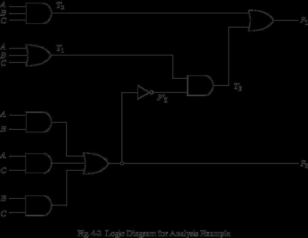
 Chapter 4 Sequential Logic Circuits 4 1 The defining characteristic of a combinational circuit is that its output depends only on the current inputs applied to the circuit. The output of a sequential circuit,
 / M Morris Mano Digital Design Ahmad_911@hotmailcom / / / / wwwuqucscom Binary Systems Introduction - Digital Systems - The Conversion Between Numbering Systems - From Binary To Decimal - Octet To Decimal
Chapter 4. Sequential Logic Circuits
 Chapter 4 Sequential Logic Circuits 1 2 Chapter 4 4 1 The defining characteristic of a combinational circuit is that its output depends only on the current inputs applied to the circuit. The output of
The Design Procedure. Output Equation Determination - Derive output equations from the state table
 The Design Procedure Specification Formulation - Obtain a state diagram or state table State Assignment - Assign binary codes to the states Flip-Flop Input Equation Determination - Select flipflop types