Digital Circuits ECS 371. Dr. Prapun Suksompong Latches and Flip-Flops
|
|
|
- Samuel Walsh
- 5 years ago
- Views:
Transcription
1 Digital Circuits ECS 371 Dr. Prapun Suksompong Latches and Flip-Flops 1
2 2 Digital Logic Circuit Types Combinational Circuit Output depends only on current inputs No feedback loops memoryless Sequential Circuit Output depends on past history plus current inputs Contains feedback loops Has memory Up to this point, we have focused on combinatorial logic circuits (i.e. the output of the circuit is dependent on the current input ONLY). Now we will shift our focus to sequential logic circuits (i.e. the output depends not only on the present input but also on the history of the input. The basic building blocks for sequential logic circuits are latches and flip-flops
3 Sequential Logic Circuits Memory is represented in the form of states. State embodies all the information about the past needed to predict current output based on current input. State variables are one or more bits of information representing logic signals in a circuit Tell you where the circuit is Used in conjunction with inputs to derive current outputs of a sequential circuit In combinational circuits, only need to look at the current inputs to get the current output. 3
4 S-R Latch A latch is a temporary storage device that has two stable states (bistable). It is a basic form of memory. The S-R (Set-Reset) latch is the most basic type. It can be constructed from NOR gates or NAND gates. With two cross-coupled NOR gates, the latch responds to active-high inputs. With two cross-coupled NAND gates, the latch responds to active-low inputs. 4


5 S-R Latch There are two versions of SET-RESET (S-R) latches. 5
6 S-R Latch (Remember This!) Two inputs S for set R for reset Two useful states (for normal operation) When output Q = 1 and Q = 0, the latch is said to be in the set state. When output Q = 0 and Q = 1, the latch is said to be in the reset state. 6
7 The Old Q - New Q Analysis R S Q Q R X new R Q S old X R Q S old Input Output S R Q new 0 0 Q old
8 The Old Q - New Q Analysis (2) S Q Q S X new S Q R old R X S Q R old Input Output S R Q new Q old 8
9 Old Q / New Q Analysis Input Output S R Q new 0 0 Q old Input Output S R Q new Q old 9
10 Expanded Version R S Q Q Input s Output s Mode S R Q Q of Operation Comment 0 0 NC NC Hold No change Reset For RESET ting Q to Set For SETting Q to Prohibited Invalid Condition S R Q Q Inputs Outputs Mode S R Q Q of Operation Comment Prohibited Invalid Condition Set For SETting Q to Reset For RESETting Q to NC NC Hold No change. 10
11 Short Version (Remember This!) R S Q Q Input S R Mode 0 0 HOLD 0 1 RESET 1 0 SET S R Q Q Inputs S R Mode 0 1 SET 1 0 RESET 1 1 HOLD 11
12 Operating S-R latch Input S R Mode 0 0 HOLD 0 1 RESET 1 0 SET Under normal conditions, both inputs of the latch remain at 0 unless the state is to be change. The application of a 1 to the S input causes the latch to go to the set state. The S input must go back to 0 before R is changed to 1 to avoid occurrence of the undefined state. Applying a 0 to S with R = 0 leaves the circuit in the same state. The application of a 1 to the R input causes the latch to go to the reset state. We can then remove the one from R, and the circuit remains in the reset state. 12
13 (1,1) Problem for S-R Latch If a 1 is applied to both the inputs of the latch, both outputs go to 0. This produces an undefined state. It results in an indeterminate or unpredictable next state when both inputs return to 0 simultaneously. In normal operation, these problems are avoided by making sure that 1 s are not applied to both inputs simultaneously. 13
14 Operating S-R latch Inputs S R Mode 0 1 SET 1 0 RESET 1 1 HOLD Under normal conditions, both inputs of the latch remain at 1 unless the state is to be change. The application of a 0 to the S input causes the latch to go to the set state. The S input must go back to 1 before R is changed to 0 to avoid occurrence of the undefined state. Applying a 1 to S with R = 1 leaves the circuit in the same state. The application of a 0 to the R input causes the latch to go to the reset state. We can then remove the 0 from R, and the circuit remains in the reset state. 14
15 Example S Q R Q 15

16 Example S Q Input s S R Mode 0 1 SET 1 0 RESET 1 1 HOLD R Q 16
17 Gated Latch A gated latch is a variation on the basic latch. The gated latch has an additional input, called enable (EN) that must be HIGH in order for the latch to respond to the S and R inputs. 17


18 Gated Latch Observe that: A S EN S EN S A Q B R EN R EN EN EN A B S R R B Q This is the same as the active-low input latch! 18
19 19 Example: Gated S-R Latch
20 Exercise: Gated S-R Latch Show the Q output with relation to the input signals. Assume Q starts LOW. S R EN Q 20
21 Gated D latch The D latch is a variation of the S-R latch. Has only one input in addition to EN. This input is called the D (data) input. Combine the S and R inputs into a single D input. D Q D Q EN EN Q Q 21

22 22 Gated D Latch: Operation A simple rule for the D latch is: Q follows D when the Enable is active/asserted. In this situation, the latch is said to be open and the path from D input to Q output is transparent. The circuit is often called a transparent latch for this reason. When EN is LOW, the state of the latch is not affected by the D input. In this situation, the latch is said to be close The Q output retains its last value and no longer changes in response to D, as long as EN remains negated. Output is latched at the last value when the enable signal becomes not asserted. Truth Table: Q 0 is the prior output level before the indicated input conditions were established. D 0 1 X Inputs EN Outputs Q 0 1 Q 0 Q 1 0 Q 0 D EN Comments RESET SET No change Q Q

23 Example: Gated D Latch Q follows D when the Enable is active. D EN Q 23 Q
24 Exercise: Gated D Latch Determine the Q output for the D latch, given the inputs shown. D EN Q Q D EN Q Notice that the Enable is not active during these times, so the output is latched. 24
25 Latch: some final words. Latch = A bistable digital circuit used for storing a bit. RESET 1. The state of a latch when the output (Q) is The action of producing a RESET state. SET 1. The state of a latch when the output (Q) is The action of producing a SET state. 25


26 Mouse button from an ancient Compaq computer Latch as a Contact-Bounce Eliminator When the contacts of any mechanical switch bang together they rebound a bit before settling, causing bounce. Debouncing is the process of removing the bounces The trigger switches from an old cheap game-playing joystick.

27 Switch Bounce Phenomenon Mechanical switch cannot be used as such to produce a clean voltage transition. The output makes several transitions between 0 and +V volts for a few milliseconds owing to contact bounce before it finally settles at +V volts. Although this random behavior lasts only for a few milliseconds, it is unacceptable for many digital circuit applications. 27
28 Contact-Bounce Eliminator (2) Key Idea: The S-R latch is in hold mode for each bounce and hence the final output does not change. 28
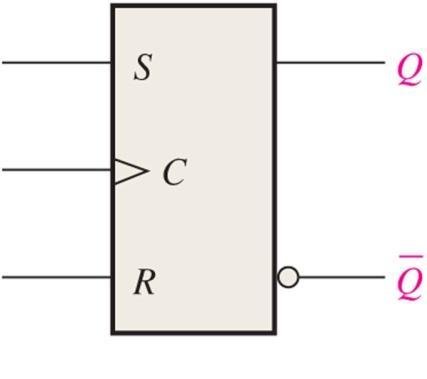
29 Logic Symbols: Latches and Flip-Flops 29
30 Flip-Flop Latches sample their inputs (and change states) any time the EN bit is asserted. Flip-flops are synchronous: the output changes state only at a specified point on the triggering input called the clock (CLK) In other words, changes in the output occur in synchronization with the clock. An edge-triggered flip-flop changes state either at the positive edge (rising edge) or at the negative edge (falling edge) of the clock pulse. 30


 Negative edge-triggered")
31 Edge-Triggered Flip-Flops Edge-triggered flipflop is redundant (all flip-flops are edgetriggered Positive edge-triggered (no bubble at C input) Negative edge-triggered (bubble at C input) 31
32 Clock (CLK) In digital synchronous systems, all waveforms are synchronized with a clock. The clock waveform itself does not carry information. The clock is a periodic waveform in which each interval between pulses (the period) equals the time for one bit. 32 Notice that change in level of waveform A occurs at the rising edge of the clock waveform.
33 D Flip-Flop The truth table for a positive-edge triggered D flip-flop shows an up arrow to remind you that it is sensitive to its D input only on the rising edge of the clock. The truth table for a negative-edge triggered D flip-flop is identical except for the direction of the arrow. D C Q Q Inputs Outputs Inputs Outputs D CLK Q Q Comments D CLK Q Q Comments SET RESET SET RESET (a) Positive-edge triggered (b) Negative-edge triggered 33 = clock transition LOW to HIGH

34 D Flip-Flop Q follows D on the rising edge of the clock 34
35 Exercise D Q CLK CLK Q What specific function does this device perform? 35
36 Exercise D Q CLK CLK Q It is a D flip-flop hardwired for a toggle mode. For example, if Q is LOW, Q is HIGH and the flip-flop will toggle on the next clock edge. Because the flip-flop only changes on the active edge, the output will only change once for each clock pulse. 36
37 D Flip Flop: Implementation Tie two D-latches together to make a D flip-flop D D Q Q M D Q C EN 1 C 2 EN Master Q Slave Q C 37 When C is 0 (C 1 = 1), the master latch is open and follows the D input. When C is 1 (C 1 = 0, C 2 = 1), the master latch is closed and its output is transferred to the slave latch. The slave latch is open all the while that C is 1, but changes only at the beginning of this interval, because the master is closed and unchanging during the rest of the interval.
38 D Flip Flop: Implementation D D Q Q M D Q C EN 1 C 2 EN Master Q Slave Q C C C1 C D Q M C2 C 38 Q

39 S-R Flip-Flop 39
40 J-K Flip-Flop Has two inputs, labeled J and K (along with the CLK). When both J and K = 1, the output changes states (toggles) on the rising clock edge. J K CLK Q Q Inputs Outputs J K CLK Q Q Comments Q 0 0 Q 0 1 No change RESET SET 1 1 Q 0 Q 0 Toggle A J-K flip-flop connected for toggle operation is sometimes called a T flip-flop. 40

41 J-K Flip-Flop 41
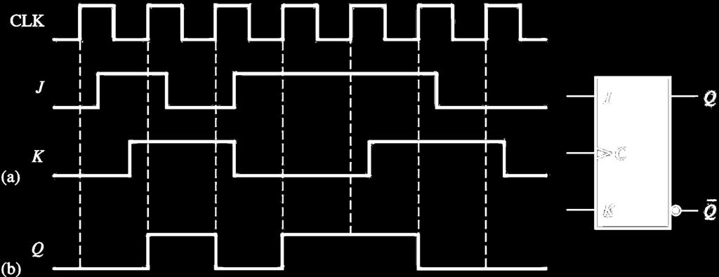
42 Exercise: J-K Flip-Flop J K CLK Q Q Inputs Outputs J K CLK Q Q Comments Q 0 0 Q 0 1 No change RESET SET 1 1 Q 0 Q 0 Toggle Set Toggle Set Latch CLK J K Q 42
43 Negative-Edge Triggered J-K FF 43
44 Caution When designing a circuit, do not change input values at the moment that the clock is rising. This is the time that the flip-flops read the input values. 44
45 Asynchronous Inputs Most flip-flops have other inputs that are asynchronous, meaning they affect the output independent of the clock. Two such inputs are normally labeled preset (PRE) and clear (CLR). These inputs are usually active-low. A J-K flip flop with active-low preset and CLR is shown. PRE J Q CLK K Q 45 CLR

46 46 Example
47 PRE Exercise J CLK Q K Q CLR CLK J K Set Toggle Set Reset Toggle Set Latch PRE CLR Reset Q 47
48 Latches and Flip-Flops The most basic storage elements are latches, from which flip-flops are usually constructed. Can maintain a binary state indefinitely (as long as power is delivered to the circuit), until directed by an input signal to switch states. The major differences among the various types of latches and flipflops are the number of inputs the process and the manner in which the inputs affect the binary state. Although latches are most often used within flip-flops, they can also be used with more complex clocking methods to implement sequential circuits directly. The design of such circuits is, however, beyond the scope of this class. 48

49 49 Logic Symbols: Latches and Flip-Flops
50 Some Applications Divide the clock frequency by 2 50

51 Some Applications Divide the clock frequency by 4 51
52 Digital Circuits ECS 371 Dr. Prapun Suksompong Counters 1
53 Counting in Binary We have seen that the binary count sequence follows a familiar pattern of 0 s and 1 s. The next bit changes on every fourth number LSB changes on every number. The next bit changes on every other number. 2
54 Counter A counter can form the same pattern of 0 s and 1 s with logic levels. The first stage in the counter represents the least significant bit (LSB) notice that these waveforms follow the same pattern as counting in binary. LSB MSB


55 4 Ex: 2-bit Asynchronous Binary Counter
56 Asynchronous counter Counters are classified into two broad categories according to the way they are clocked: 1. Asynchronous counter 2. Synchronous counter The term asynchronous refers to events that do not have a fixed time relationship with each other and, generally, do not occur at the same time. Asynchronous counters The FFs within the counter do not change states at exactly the same time because they do not have a common clock pulse. 5
.")
57 Asynchronous counter (con t) Commonly called ripple counters The FFs are connected for toggle operation (J = 1, K = 1) The first FF is clocked by the external clock pulse (CLK). Each successive FF is clocked by the output of the preceding FF. 6
58 Ex: 3-bit Asynchronous Counter HIGH J 0 Q 0 J Q 1 1 J Q 2 2 CLK C C C K 0 Q 0 Q 1 K 1 K 2 (LSB) CLK Q Q (MSB) Q Recycle back to 0
 Q 2 0 0 0 0 1 1 1 1 0 The second flipflop is triggered by the negativeedges of Q 0.")
59 Ex: 3-bit Asynchronous Counter HIGH J 0 Q 0 J Q 1 1 J Q 2 2 CLK C C C K 0 Q 0 Q 1 K 1 K 2 CLK (LSB) Q Q (MSB) Q The second flipflop is triggered by the negativeedges of Q 0.
 Q 2 0 0 0 0 1 1 1 1 0 The third flip-flop is triggered by the negative-edges of Q 1.")
60 Ex: 3-bit Asynchronous Counter HIGH J 0 Q 0 J Q 1 1 J Q 2 2 CLK C C C K 0 Q 0 Q 1 K 1 K 2 CLK (LSB) Q Q (MSB) Q The third flip-flop is triggered by the negative-edges of Q 1.


61 Ex: Four-bit binary ripple counter. 10

62 (Also called asynchronous counter or serial counter) Summary: n-bit Binary Ripple Counter Use a cascaded arrangement of FFs where the output of one flipflop drives the clock input of the following flip-flop. The clock input is applied only to the first FF, also called the input FF. The clock input to any subsequent FF comes from the output of its immediately preceding flip-flop. After the occurrence of each clock input pulse, the counter has to wait for a time period equal to the sum of propagation delays of all flip-flops before the next clock pulse can be applied. 11
63 Modulus The modulus (MOD number) of a counter is the number of unique (logic) states through which the counter will sequence. The maximum possible number of states (maximum modulus) of a counter is 2 n, where n is the number of FFs in the counter. An n-bit counter that counts through all its natural states and does not skip any of the states has a modulus of 2 n. Counters can be designed to have a number of states in their sequence that is less than the maximum of 2 n. This type of sequence is called a truncated sequence. To obtain a truncated sequence, it is necessary to force the counter to recycle before going through all of its possible states. 12
64 Counters with Truncated Sequences One common modulus for counters with truncated sequences is ten (called MOD10). Counters with ten states in their sequence are called decade counters. A decade counter with a count sequence of zero (0000) through nine (1001) is a BCD decade counter because its ten-state sequence produces the BCD code. The BCD decade counter must recycle back to the 0000 state after the 1001 state. We will use a technique called partial decoding. 13

65 BCD Decade Counter (1) A decade counter requires four FFs. Three FFs are insufficient because 2 3 = 8. Start with 4-bit asynchronous binary counter Want to recycle here!


66 BCD Decade Counter (2) This is used to detect the number 10 When Q 1 and Q 3 are HIGH together, the counter is cleared by a glitch on the CLR line
67 Q 3 Q 2 Q 1 Q BCD Decade Counter (3) One way to make the counter recycle after the count of nine (1001) is to decode count ten (1010) with a NAND gate and connect the output of the NAND gate to the active-low CLR inputs of the FFs. Partial Decoding: In our circuit, only Q 1 and Q 3 are connected to the NAND gate inputs. The two unique states (Q l = 1 and Q 3 = 1) are sufficient to decode the count of ten because none of the other states (zero through nine) have both Q l and Q 3 HIGH at the same time. HIGH CLK J 0 Q 0 K 0 Q 1 Q 2 J 1 J 2 C C C K 1 K 2 J 3 C K 3 Q 3 10 Decoder CLR
68 K-Map Derivation of Partial Decoding Q 3 Q 2 Q 1 Q 0 CLR X X X X X Q X X 0 0 Q 0 Q X X X 1 Q 2 QQ
69 Ex: MOD12 Counter Q 3 Q 2 Q 1 Q
70 74x93 4-Bit Asynchronous Binary Counter Consist of single flip-flop and a 3-bit asynchronous counter. 19
 and RO(2).")
71 74x93 The counter can be extended to form a 4-bit counter by connecting Q 0 to the CLK B input. Provide gated reset inputs, RO(1) and RO(2). When both of these inputs are HIGH, the counter is reset to the 0000 state. 20


72 74x93 Applications 74x93 as a MOD10 counter 74x93 as a MOD16 counter Exercise: Show how to connect a 74x93 4-bit asynchronous counter as a MOD12 counter. 74x93 as a MOD12 counter 21 The qualifying label CTR DIV N indicates a counter with N states.
73 Synchronous Counters The term synchronous refers to events that have a fixed time relationship with each other. A synchronous counter is one in which all the flip-flops in the counter are clocked at the same time by a common clock pulse. Hence, all FFs in the counter change state at the same time in synchronism with the input clock signal. Also known as a parallel counter. Synchronous counters overcome the disadvantage of accumulated propagation delays, but generally they require more circuitry to control states changes. 22
74 Caution! The analysis and design of synchronous counter is significantly different from the analysis and design of asynchronous counter Recall: Suppose we want to count from 0 to 9. For asynchronous counter, we let the number 10 shows up first, we detect it with a simple decoder, then we use the detection to asynchronously clear all the FFs back to 0. In other words, the number 10 actually shows up on the output but only for a short time (so short that you many not see it in the real circuit.) 23
75 Synchronous Counters (2) We won t use the same technique (of asynchronously zeroing all FFs) in synchronous design. Reason: It is asynchronous! We want to change the value of the states/outputs of the FFs only at the rising edge of the clock. In other words, if we let the number 10 shows up, it will be there until the next rising edge of the clock. So, we need to come up with a new technique. Tabular analysis. 24
76 Caution! We will study two techniques. The first technique (tabular analysis) is here to give you some intuition about the more-general second technique. Once we are done with the first technique, we will move on to the second technique and will not use the first technique anymore! 25
77 26 Ex: 2-Bit Synchronous Binary Counter
78 Summary of Analysis 1. Find the equations that govern the relationship between the FF inputs (J i, K i ) and the FF outputs (states: Q i ). 2. Start with a relevant arbitrary state (combination of outputs). We will start with a state where every Q i is Calculate the value of the inputs (J i, K i ) of all FFs. This tell us the modes of the FFs. 4. Find the next state (combination of outputs of the FFs) at the next clock pulse from the modes. 5. Repeat the last two steps until the counter recycles. 27 Outputs J-K Inputs Q 1 Q 0 J1 Q0 K1 Q0 J 0 1 K
79 Ex: 3-bit Binary Synchronous Counter This 3-bit binary synchronous counter has the same count sequence as the 3-bit asynchronous counter shown previously. HIGH Q 0 J 0 Q 0 Q 1 Q 0 Q J 1 Q 1 J 2 2 C C C K 0 K 1 K 2 CLK 28
80 Analysis of Synchronous Counters A tabular technique for analysis is illustrated for the counter on the previous slide. (1) Write the logic equation for each input. (2) Put the counter in an arbitrary state; then (3) determine the inputs for this state. Outputs (4) Use the new inputs to determine the next state: Q 2 and Q 1 will latch and Q 0 will toggle. Logic for inputs (5) Set up the next group of inputs from the current output. Q 2 Q 1 Q 0 J 2 = Q 0 Q 1 K 2 = Q 0 Q 1 J 1 = Q 0 K 1 = Q 0 J 0 = 1 K 0 = (6) Q 2 will latch again but both Q 1 and Q 0 will toggle. (7) Continue like this, to complete the table. The next slide shows the completed table 29
81 Analysis of Synchronous Counters Outputs Logic for inputs Q 2 Q 1 Q 0 J 2 = Q 0 Q 1 K 2 = Q 0 Q 1 J 1 = Q 0 K 1 = Q 0 J 0 = 1 K 0 = At this point all states have been accounted for and the counter is ready to recycle


82 4-bit Synchronous Binary Counter The 4-bit binary counter has one more AND gate than the 3-bit counter just described. The shaded areas show where the AND gate outputs are HIGH causing the next FF to toggle. 31
83 BCD Decade Counter With some additional logic, a binary counter can be converted to a BCD synchronous decade counter. After reaching the count 1001, the counter recycles to HIGH Q 3 Q 0 FF0 FF1 FF2 FF3 J 0 Q 0 J 1 Q 1 J 2 Q 2 J 3 Q 3 C C C C Q 3 K 0 Q 0 K 1 Q 1 K 2 Q 2 K 3 Q 3 CLK 32
84 BCD Decade Counter: Tabular Analysis Q 3 Q 2 Q 1 Q 0 J3 K3 Q0Q3 Q0Q1 Q2 J2 K2 Q0Q1 J1 K1 Q0 Q J 3 0 K
85 BCD Decade Counter: Tabular Analysis Q 3 Q 2 Q 1 Q 0 J3 K3 Q0Q3 Q0Q1 Q2 J2 K2 Q0Q1 J1 K1 Q0 Q3 J0 K
86 BCD Decade Counter Design The previous slide shows that the given design works. How can we get it in the first place? In particular, where do these logic parts come from? HIGH Q 3 Q 0 FF0 FF1 FF2 FF3 J 0 Q 0 J 1 Q 1 J 2 Q 2 J 3 Q 3 C C C C Q 3 K 0 Q 0 K 1 Q 1 K 2 Q 2 K 3 Q 3 CLK 35
87 BCD Decade Counter: Derivation Q 3 Q 2 Q 1 Q 0 J3 K J2 K2 J1 K1 J0 K0 36
88 BCD Decade Counter: Derivation Q 3 Q 2 Q 1 Q 0 J3 K3 J2 K2 J1 K1 J K
89 Recall: Truth Table v.s. K-map Input Columns A B C X AB A C C B Output Column 38
90 Row # Row # Recall: Karnaugh Map AB C C 1 AB CD C A A B C B A The small number inside each cell is the corresponding row number in the truth table, assuming that the truth table inputs are labeled alphabetically from left to right (e.g. A, B, C) and the rows are numbered in binary counting order. D B A B C D
91 BCD Decade Counter: Derivation Q 3 Q 2 Q 1 Q 0 J 3 K 3 J2 K2 J1 K1 J K Q 1 Q 1 Q Q 2 Q 2 Q 2 X X X X X X X X X X X X Q 3 Q 3 Q X X 0 0 X X 0 0 X X 40 Q 0 Q 0 Q 0
92 Caution! Now we are done with the first technique for designing counter. It is a fine technique but have some disadvantages: 1. We need to work on the row-by-row basis. (The formula are defined column-wise; so it seems that working with columns might be faster.) 2. We assume that we start from 0, find the next state (on the next row), and then keep finding the next state until we get back to 0, at which point we stop. What would happen if we stat from a state which is not in the sequence above? 3. We assume that J = K. Can we have a simpler circuit if we don t use this assumption. After we study 74x163, we will move on to the second technique and will not use the first technique anymore! 41
93 Data inputs 42 74x163 4-bit Synchronous Binary Counter Has several extra features Can be synchronously preset to any 4-bit binary number when the active-low LOAD input is activated. The active-low clear input (CLR) synchronously resets all four FFs. The two enable inputs, ENP and ENT must both be HIGH for the counter to sequence through its binary states. CLR LOAD ENT ENP CLK (1) (9) (10) (7) (2) C D 0 D 1 D 2 D 3 (3) (4) (5) (6) CTR DIV 16 TC = 15 (15) (14) (13) (12) (11) Q 0 Q 1 Q 2 Q 3 Data outputs The ripple clock output (RCO) goes HIGH when the counter reaches the last state in its sequence of fifteen, called the terminal count (TC = 15). RCO
94 43 Example: 74x163
95 Example: 74x163 44
96 Example: 74x163 45
97 Example: 74x163 Copied 46
 goes HIGH when the counter reaches")

98 Example: 74x163 The ripple clock output (RCO) goes HIGH when the counter reaches the last state in its sequence of fifteen, called the terminal count (TC = 15). 47
99 Example: 74x163 48
100 49 74x163: Logic Diagram
101 50 74x163: State Table
102 74x163: Application Count from 0 to 10. Then, repeat. 51
103 74x163: Application Count from 5 to 15. Then, repeat. 52
104 Exercise What will this counter do? 53
105 Caution! Now, we will present the second technique for designing counter. This technique is general enough for designing any sequential circuit. It is different from the first technique in many ways. We start by listing all the possible states For each state, we find out what would be the next state. In particular, for the first technique, we find out the next state by looking at the state value in the row below. This is not true for the second technique. The next states are listed on the column to the right. 54
106 Counter Design Technique We want to design counters with arbitrary sequences. Today, we will discuss in detail a commonly used technique for designing synchronous counters using J-K flip-flops or D flipflops. The design of the counters basically involves designing a suitable combinational logic circuit that takes its inputs from the normal and complemented outputs of the FFs used and decodes the different states of the counter to generate the correct logic states for the inputs of the FFs such as J, K, D, etc. We will start by learning sequential circuit design techniques. 55
107 Sequential Circuits Also known as state machine. A general sequential circuit consists of a combinational logic section and a memory section (FFs). In a clocked sequential circuit, there is a clock input to the memory section. 56
108 Sequential Circuits At any given time, the memory is in a state called the present/current state. The present state is represented by the state variables (Q 0, Q 1, Q 2, Q 3, ) It will advance to the next state on the clock pulse. The next state is determined by the conditions on the excitation lines and the current sate. 57
109 State Transition Diagram The state transition diagram is a graphical representation of different states of a given sequential circuit and the sequence in which these states occur in response to a clock input. Different states are represented by circles, and the arrows joining them indicate the sequence in which different states occur. Ex. State transition diagram for a MOD-8 binary counter. 58
110 Step 1: State Diagram Specify the counter sequence and draw a state diagram. As an example, here is a state diagram for a 3-bit Gray code counter
111 Step 2: Next-State Table List each state of the counter (current state) along with the corresponding next state Present State Q 2 Q 1 Q 0 Next State Q 2 Q 1 Q
112 Step 3: FF Excitation Inputs Find the J and K inputs required for the transitions in the Next-State Table Current State Next State FF 2 FF 1 FF 0 Q 2 Q 1 Q 0 Q 2 Q 1 Q 0 J 2 K 2 J 1 K 1 J 0 K
113 Step 3: FF Excitation Inputs Find the J and K inputs required for the transitions in the Next-State Table Rearranged to our familiar form Current State Next State FF 2 FF 1 FF 0 Q 2 Q 1 Q 0 Q 2 Q 1 Q 0 J 2 K 2 J 1 K 1 J 0 K We will first develop a transition table showing the FF inputs required for each transition.
114 FF Excitation/Transition Table The excitation table lists the present state, the desired next state and the flip-flop inputs (J, K, D, etc.) required to achieve that. Excitation table of a J-K flip-flop. Excitation table of a D flip-flop. An X indicates a don't care (the input can be either a 1 or a 0). 63 The transition table is always the same for a given type of flip-flop.
115 Step 3: Find Excitation Inputs to FFs For the current state 000, Q 0 goes from a present state of 0 to a next state of 1. To make this happen, J 0 must be a 1 and you don't care what K 0 is (J 0 = 1, K 0 = X), Output Transitions Q N Q N Flip-Flop Inputs J K 0 X 1 X X 1 X 0 Current State Next State FF 2 FF 1 FF 0 Q 2 Q 1 Q 0 Q 2 Q 1 Q 0 J 2 K 2 J 1 K 1 J 0 K X X X X X X X X 0 64
116 Step 3: Find Excitation Inputs to FFs Output Transitions Q N Q N Flip-Flop Inputs J K 0 X 1 X X 1 X 0 Current State Next State FF 2 FF 1 FF 0 Q 2 Q 1 Q 0 Q 2 Q 1 Q 0 J 2 K 2 J 1 K 1 J 0 K X 0 X 1 X X 1 X X X X 0 0 X X X 0 X X 1 0 X 0 X X 0 0 X X X 0 X 0 1 X X 0 X 1 X 0 65

117 Step 4: Karnaugh Maps Karnaugh maps can be used to determine the logic required for the J and K inputs of each flip-flop. FF 0 J 0 K 0 1 X X 0 0 X X 1 0 X X 1 1 X X There is a Karnaugh map for each input of each FF.
118 Row # Row # Review: Karnaugh Map AB C C 1 AB CD C A A B C B A The small number inside each cell is the corresponding row number in the truth table, assuming that the truth table inputs are labeled alphabetically from left to right (e.g. A, B, C) and the rows are numbered in binary counting order. D B A B C D
119 Step 5: Logic Expressions for FF Inputs From the Karnaugh maps, we group the cells to generate the logic expression for each FF input: J Q Q Q Q Q Q K Q Q Q Q Q Q J K J Q Q Q Q Q Q K Q Q

120 J Q Q K Q Q J K J Q Q Step 6: Counter Implementation Q Q Q Q K Q Q Implement the expressions with combinational logic, and combine with the FFs to create the counter. 69
121 Example: Arbitrary Counting Sequence 0 2 D 0 Q 0 CLK C 1 Method 1: Use D FFs Q 0 Current State Next State FF 1 FF 0 Q 1 Q 0 Q 1 Q 0 D 1 D X X X X 70 D D Q Q Q 0 1 D 1 Q K-maps C Q 1 3 Check Answer 1 Current State FF 1 FF 0 Next State Q 1 Q 0 D1 Q1 Q D 0 0 Q1 Q 1 Q

122 Example: Arbitrary Counting Sequence Method 2: Use J-K FFs CLK 1 J 0 Q 0 C K 0 Q 0 71 Current State Next State FF 1 FF 2 Q 1 Q 0 Q 1 Q 0 J 1 K 1 J 0 K X 0 X X X X 1 1 X 1 1 X X X X X X K-maps J K J K Q 1 Q 1 J 1 Q 1 C K 1 Q 1
123 CLK 1 Example: Check Answer J 0 Q 0 C K 0 Q 0 Current State FF 1 FF 2 Next State Q 1 Q 0 J1 Q0 K1 1 J0 Q1 K0 1 Q 1 Q J 1 Q 1 C K 1 Q
124 Example: Comparison Method 1: Use D FFs 3 1 D 0 Q 0 Method 2: Use J-K FFs J 0 Q 0 CLK C 1 CLK C 1 K 0 Q 0 Q 0 J 1 Q 1 73 D 1 Q 1 C Q 1 C K 1 Q 1
125 Exercise Design a counter which satisfies all of the following requirements: 1. Have one-bit input signal called CTEN. 2. Have three-bit output signal called Y2, Y1, Y0. 3. The counting sequence agrees with the following state diagram: The numbers on the arrows indicate the values of CTEN. 4. Use exactly one D flip-flop and one XOR gate. 5. No additional gate allowed
126 Exercise Expected Waveform:

127 76 Solution


128 Sequential Circuits In general, sequential circuits can be classified into two types 1. Moore circuits: the output(s) depend only on the present internal state 2. Mealy circuits: the output(s) depend on both the present state and the input(s). 77
129 Synchronous Cascading Use 1. count enable (CTEN) On some devices, CTEN is labeled as G 2. terminal count (TC) Same as ripple clock output (RCO) on some IC counters The next counter is enabled only when the TC of the previous stage is reached. 78

130 Cascaded Counters Cascading is a method of achieving higher-modulus counters. In essence, cascading means that the last-stage output of one counter drives the input of the next counter. Asynchronous Cascading: 79
 Same as ripple clock output (RCO) on some IC counters The next counter is enabled only when the TC of")
131 Synchronous Cascading Use 1. count enable (CTEN) On some devices, CTEN is labeled as G 2. terminal count (TC) Same as ripple clock output (RCO) on some IC counters The next counter is enabled only when the TC of the previous stage is reached. 80

132 Example: Determine the overall modulus of the following cascaded counters: The over all modulus is The over all modulus is

133 82 Application: Digital Clock
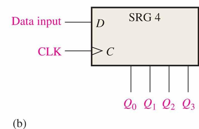
134 Digital Circuits ECS 371 Dr. Prapun Suksompong Shift Registers 1
135 Register Flip-flops are used in a variety of application circuits, the most common among these being counting circuits and frequency division and data storage and transfer (data movement) circuits. Counters and registers Belong to the category of MSI sequential logic circuits. Similar architecture: both comprise a cascaded arrangement of more than one FFs. Both constitute very important building blocks of sequential logic 2
136 Register A register, unlike a counter, has no specified sequence of states, except in certain very specialized applications. Application Counters are mainly used in counting applications, where they either measure the time interval between two unknown time instants or measure the frequency of a given signal. Registers are primarily used for the temporary storage of data present at the output of a digital circuit before they are fed to another digital circuit. 3
137 Register and Shift Register The storage capacity of a register is the total number of bits (1s and 0s) of digital data it can retain. Since each FF can store one bit of data, the storage capacity of the shift register equals the number of FFs used. The shift capability of a register permits the movement of data from stage to stage within the register or into or out of the register upon application of clock pulses. 4
138 Shift Register A shift register is an arrangement of flip-flops with important applications in storage and movement of data. Some basic data movements are illustrated here. Data in Data in Data out Data out Data in Data out Serial in/shift right/serial out Serial in/shift left/serial out Parallel in/serial out SISO SISO PISO Data in Data in 5 SIPO PIPO Data out Data out Serial in/parallel out Parallel in/parallel out Rotate right Rotate left The basic building block in all shift registers is the FF, mainly a D-FF. Although in many of the commercial shift register ICs their internal circuit diagram might indicate the use of S-R FFs, a careful examination will reveal that these S- R FFs have been wired as D FFs only.
139 Serial-in/Serial out Shift Register Accept data serially: one bit at a time on a single line. Each clock pulse will move an input bit to the next FF. For example, a 1 is shown as it moves across. Five-bit serial-in serial-out register. Serial data input FF0 FF1 FF2 FF3 FF4 Serial D 0 Q 0 D 1 Q 1 D 2 Q 2 D 3 Q 3 D 4 Q 4 data output C C C C C CLK CLK 6
140 Basic Application: SIPO An application of shift registers is conversion of serial data to parallel form. For example, assume the binary number 1101 is loaded sequentially, one bit at each clock pulse. Serial data input FF0 FF1 FF2 D 0 Q 0 D 1 Q 1 D 2 Q 2 D 3 Q 3 C C C C FF3 X CLK CLK After 4 clock pulses, the data is available at the parallel output. They can be stored for any length of time as long as the FFs have dc power.

141 8 SIPO Shift Register
142 9 PISO Shift Register

143 10 PIPO Shift Register
144 Digital Circuits ECS 371 Dr. Prapun Suksompong Memory and Storage 1
145 Memory Memory is the portion of a computer or other system that stores binary data. The smallest unit of binary data, as you know, is the bit. In many applications, data are handled in an 8-bit unit called a byte. Each storage element in a memory can retain either a 1 or a 0 and is called a cell. 2
146 Memory Capacity The term word can have two meanings in computer terminology. In memories, it is defined as a group of bits or bytes that acts as a single entity that can be stored in one memory location. In assembly language, a word is specifically defined as two bytes. A memory is identified by the number of words it can store times the word size. A 16k 8 memory can store 16,384 words of eight bits each. The capacity of a memory is the total number of data units that can be stored. 3

147 64 1 Memory Address The location of a unit of data in a memory is called the address

148 Memory Address (2) 64 8 The address depends on how the memory is organized into units of data. Personal computers have random-access memories organized in bytes. The smallest group of bits that can be addressed is eight. 5
149 Basic Memory Operations The write operation puts data into a specified address in the memory. The read operation copies data out of a specified address in the memory. The addressing operation, which is part of both the write and the read operations, selects the specified memory address. 6
150 Data Bus Data units go into the memory during a write operation and come out of the memory during a read operation on a set of lines called the data bus. The data bus is bidirectional, which means that data can go in either direction (into the memory or out of the memory). 7

151 Address Bus For a write or a read operation, an address is selected by placing a binary code representing the desired address on a set of lines called the address bus. The number of lines in the address bus depends on the capacity of the memory bit address code can select 65,536 locations (2 16 ) in the memory 32-bit address code can select 4,294,967,296 (4G) locations (2 32 ) in the memory

152 9 3D Memory Array
153 10 Simplified Write Operation

154 11 Simplified Read Operation
155 Categories RAM DRAM SRAM Memory ROM EPROM PROM EEPROM Hybrid NVRAM Flash EEPROM Mask 12


156 RAM: Random-Access Memory All addresses are accessible in an equal amount of time and can be selected in any order for a read or write operation. This is in contrast to sequential memory devices such as magnetic tapes in which the mechanical movement of the storage medium forces the computer to access data in a fixed order. All RAMs have both read and write capability. Volatile: lose stored data when the power is turned off. Typically used for short-term data storage Two major categories of RAM 1. Static RAM (SRAM) 2. Dynamic RAM (DRAM) 13
157 Computer Memory People in the computer industry commonly use the term memory to refer to RAM A computer uses RAM to hold temporary instructions and data needed to complete tasks. This enables the computer s CPU (Central Processing Unit), to access instructions and data stored in memory very quickly. These days, no matter how much memory your computer has, it never seems to be quite enough. In 1981, referring to computer memory, Bill Gates said, 640K (roughly 1/2 of a megabyte) ought to be enough for anybody. 14

158 15 RAM Family
159 SRAM and DRAM Two major categories of RAM 1. Static RAM (SRAM) Generally use latches as storage elements Can store data indefinitely as long as dc power is applied. 2. Dynamic RAM (DRAM) Use capacitors as storage elements Can not retain data very long without the capacitors being recharged by a process called refreshing. Data can be read much faster from SRAMs DRAMs can store much more data for a given physical size and cost because the DRAM cell is much simpler, and more cells can be crammed into a given chip area than in the SRAM. 16
160 SRAM and DRAM (2) The first SRAM (256-bit) and DRAM (1024-bit) devices were both created in For the next few decades, both types of memory quadrupled their capacities approximately every three years, but by the beginning of the 21st century this had slowed to a doubling every two to three years. These days, DRAM (in its SDRAM incarnation) is used to satisfy the bulk of a system s RAM requirements, while SRAM is used where speed is of the essence; for example, the cache memory inside a CPU. 17
161 Address Multiplexing DRAMs use a technique called address multiplexing to reduce the number of address lines. For example, consider a DRAM which have 10 address lines. The ten address lines are time multiplexed at the beginning of a memory cycle into two separate 10-bit address fields: the row address and the column address. First, the l0-bit row address is latched into the row address latch. Next, the l0-bit column address is latched into the column address latch. The row address and the column address are decoded to select one of the 1,048,576 addresses (2 20 ) in the memory array. 18
162 ROM: Read-only Memory Nonvolatile: Retain stored data even if power is turned off Data are stored permanently or semi-permanently. Data can be read from a ROM, but there is no write operation as in the RAM. The ROM, like the RAM, is a random-access memory but the term RAM traditionally means a random-access read/write memory. 19

163 Memory Expansion: Word-Length Memory can be expanded in either word length or word capacity or both. Word-Length Expansion: the #bits in the data bus is increased Example: One ROM from two ROMs 20

164 Word-Length Expansion (con t) Example: One 2 m 2n RAM from two 2 m n RAMs 21

165 Word-Capacity Expansion When memories are expanded to increase the word capacity, the number of addresses is increased. 22


")
166 Storage Storage media are important, particularly in computer applications, where they are used for mass nonvolatile storage of data and programs. Hard disk Magnetic Storage Magnetic Disk Tape Floppy disk Zip disk Storage CD-R (Recordable) Optical (Laser) Storage CD-RW (Rewritable) 23 DVD-ROM
167 Spelling: Disc vs Disk Compact disc (CD) is spelled with a C A computer hard disk is spelled with a K Disks are usually sealed inside a metal or plastic casing (often, a disk and its enclosing mechanism are collectively known as a "hard drive"). In modern technological contexts, A disc refers to optical media, such as an audio CD, CD-ROM, DVD-ROM, DVD-RAM, or DVD-Video disc A disk refers to magnetic media, such as a floppy disk, the disk in your computer's hard drive, an external hard drive. 24
168 CD: Layers All optical media is constructed of layers of different materials. The information is recorded as a series of pits (or bumps) on a polycarbonate substrate roughly 1.2 mm thick The pits are coated with a thin layer of Al or gold (few 100s nm thick) and then protected by a 2-30 m shellac (lacquer) coating. The lacquer coating is screen printed. 25
169 CD: Effect of Scratches The bottom of a CD is made of a relatively thick piece of polycarbonate plastic. Scratches on the polycarbonate are out of focus when the disc is read, and minor scratches are ignored completely. It takes a deep scratch in the polycarbonate to affect the readability of a disc. The top is protected by a thin coat of lacquer. Even a small scratch in the lacquer can damage the reflector. Scratching the top of a disc can render it unreadable, which is something to consider the next time you place a disc on your desk top-down to protect it. 26


170 CD: Pits and Spiral The basic principle of storing data on a CD (and DVD) is the creation of pits and lands, which are translated into ones and zeros by a laser pickup head. Pits are arranged as a single spiral. This spiral is over 3.7 miles (or 6 km) in length on a CD, and 7.8 miles (or 12.5 km) for a DVD. The starting point for the spiral is towards the center of the disc with the spiral extending outward. Outer area: generally more prone to manufacturing defects Facilitate adoption of smaller or larger diameter discs 27
171 CD: Pits and Spiral (2) The disc is read and written from the inside out, which is the opposite of how hard drives organize data. With spiral organization, there are no cylinders or tracks like those on a hard drive. (The term track refers to a grouping of data for optical media.) The information along the spiral is spaced linearly, thus following a predictable timing. Spiral contains more information at the outer edge of the disc than at the beginning. If this information is to be read at a constant speed, the rotation of the disc must change between different points along the spiral. 28
172 CD: Some rough calculation Playing time: 74 minutes and 33 seconds max (4473 sec) Back-of-the-Envelope Calculation: Original audio (data) bit rate bit channel samples bits k channel sample sec sec Disc Capacity bits secs bits bytes sec CD CD CD 9 1.4M M 29
173 CD and DVD Little has changed in CD physics since the origin of CD audio discs in Maintain physical compatibility with an established base of installed units The structure of CD media was both groundbreaking and nearly ideal for this function. DVDs are an evolutionary growth of CD s with slight changes. Considering the development of DVD follows the CD by 14 years, you can see that the CD was truly a revolutionary creation in its time. 30
174 DVD: Introduction No single company owns DVD. The official specification was developed by a consortium of ten companies Hitachi, JVC, Matsushita, Mitsubishi, Philips, Pioneer, Sony, Thomson, Time Warner, and Toshiba. In May 1997, the DVD Consortium was replaced by the DVD Forum Q: What Does DVD Stand For? A: Nothing. The original meaning was digital videodisk. Some members of the DVD Forum have pointed out that DVD goes far beyond video and have offered the painfully contorted phrase digital versatile disc as a solution, but this has never been officially accepted by the DVD Forum. The DVD Forum decreed in 1999 that DVD, as an international standard, is simply three letters. 31

 Hold 4.")

 Reduce the size")


175 DVD: Capacity Increase Introduced in the U.S. in 1997 Use the same diameter platter as a CD (120mm/4.75" diameter) Hold 4.7GB rather than 700MB. Use laser beam with a shorter wavelength (650 or 635 nm, compared with 780 nm for the CD) Reduce the size of the beam spot Allow the laser to focus on a smaller pit size and a closer track pitch Pit length and track pitch are about half of CD s 4x capacity More efficient recording algorithms (Mathematics) more capacity increase 32

176 DVD: Capacity (2) Unlike the CD, which has one substrate, the DVD consists of two 0.6-mm thick substrates bonded back-to-back, which gives it the necessary stiffness to avoid disc wobble or tilt. DVDs may record data on one side only (single-sided) or on both sides (double-sided). Each side may have a single layer of recording or two layers (dual-layer) 33
177 34 DVD Mastering and Stamping


178 Blu-ray Disc Introduced in 2006 The Blu-ray name is a combination of "blue," for the color of the laser that is used, and "ray," for optical ray. The "e" in "blue" was purposefully left off because an everyday word cannot be trademarked. 35

179 Electromagnetic Spectrum nm 400 nm

 instead of a red laser")
180 Blu-Ray Disc DVD: 5x to 10x storage capacity of CD Blu-ray Disc: 5x to 10x storage capacity of DVD Use of a blue laser (which is where the format gets its name) instead of a red laser 37
181 Digital Circuits ECS 371 Dr. Prapun Suksompong Digitization 1


182 Converting Analog Signals to Digital The real world is analog! Interfacing between analog and digital is important. Digitization 1. Sampling (and hold): Discretize the time Get sampled values of the analog signal. 2. Quantization: Discretize quantity values Convert each sampled value to a binary code. 2
183 Digitization (analog to digital) Vertical lines are used for sampling Horizontal lines are used for quantization Time

184 Simplified block diagram of a digital cellular phone 4
185 Digitization = loss of information? At first glance, digitization of a continuous signal (audio, image) appears to be an enormous loss of information, because a continuous function is reduced to a function on a grid of points. Therefore the crucial question arises as to which criterion we can use to ensure that the sampled points are a valid representation of the continuous signal, i.e., there is no loss of information. 5
186 Sampling Sampling is the process of taking a sufficient number of discrete values of points on a waveform that will define the shape of wave form. Suppose that we sample a signal at a uniform rate, once every T s seconds. We refer to Ts as the sampling period, and to its reciprocal f s = 1/T s as the sampling rate. The more samples you take, the more accurately you can define a waveform. Caution: If the sampling rate is too low, your may experience distortion (aliasing). 6
187 Example This is the plot of sin(100 t). What s wrong with it? t 7
188 Example (con t) Signal of the form sin 2 ft 0 So, the frequency of sin 100 t is 50 Hz. have frequency f f0 Hz. From time 0 to 1, it should have completed 50 cycles. However, our plot has only one cycle. It looks more like a plot of sin 2 t t
189 Example (con t) 1 Aliasing causes high-frequency signal to be seen as low frequency t t
190 Spectrum We have been an example of a signal which contains only one frequency. Analog signals (sound, image, etc) usually contain a spectrum of component frequencies. Periodic signal can be expressed in terms of its components via Fourier series. In general, signal can be expressed in terms of its components via Fourier transform. 10
191 Fourier Series 11
192 Example Consider the following analog signal Time 12
193 Example It can be written as cos 2 2cos 4 sin 2 x t t t t Time 13
194 Component Frequencies f 1 f 2 f 1 cos 2 2cos 4 sin 2 x t t t t Time


195 Spectrum: Light A source of light can have many colors mixed together and in different amounts (intensities). 15 A rainbow, or prism, sends the different frequencies in different directions, making them individually visible at different angles.
196 Power/frequency (db/hz) Frequency (Hz) Spectrum: Sound 1 sin(c*erf(t)) sin(c*erf(t)) Time in seconds sin(c*erf(t)) Time MATLAB s demo Frequency (khz)

197 Spectrum: Voice 17
198 Sampling Theorem In order to (correctly and completely) represent an analog signal, the sampling frequency, f s, must be at least twice the highest frequency component of the analog signal. Given a sampling frequency, f s, the Nyquist frequency is defined as f s /2. If you've ever watched a film and seen the wheel of a rolling wagon appear to be going backwards, you've witnessed aliasing. The movie's frame rate isn't adequate to describe the rotational frequency of the wheel, and our eyes are deceived by the misinformation! 18
199 Example (revisited) Signal of the form sin 2 ft 0 So, the frequency of sin 100 t is 50 Hz. have frequency f f0 Hz. We need to sample at least 100 times per time unit. Here, the number of sample per time unit is 49, which is too small to avoid aliasing t

200 Demonstration of Aliasing of a Sinusoidal Signal 20
201 Quantization 21

202 22 Quantization
Digital Circuits ECS 371
 Digital Circuits ECS 371 Dr. Prapun Suksompong prapun@siit.tu.ac.th Lecture 18 Office Hours: BKD 3601-7 Monday 9:00-10:30, 1:30-3:30 Tuesday 10:30-11:30 1 Announcement Reading Assignment: Chapter 7: 7-1,
CHW 261: Logic Design
 CHW 26: Logic Design Instructors: Prof. Hala Zayed Dr. Ahmed Shalaby http://www.bu.edu.eg/staff/halazayed4 http://bu.edu.eg/staff/ahmedshalaby4# Slide Digital Fundamentals CHAPTER 8 Counters Slide 2 Counting
Digital Fundamentals
 Digital Fundamentals Tenth Edition Floyd Chapter 9 Sections 9-1 thru 9-5 2009 Pearson Education, Upper 2008 Pearson Saddle River, Education NJ 07458. All Rights Reserved ET285 Agenda Week 2 Quiz 0: Covered
PGT104 Digital Electronics. PGT104 Digital Electronics
 1 Part 6 Sequential Logic ircuits Disclaimer: Most of the contents (if not all) are extracted from resources available for Digital Fundamentals 10 th Edition 2 Basic Shift Register Operations A shift register
LOGIC CIRCUITS. Basic Experiment and Design of Electronics
 Basic Experiment and Design of Electronics LOGIC CIRCUITS Ho Kyung Kim, Ph.D. hokyung@pusan.ac.kr School of Mechanical Engineering Pusan National University Outline Combinational logic circuits Output
LOGIC CIRCUITS. Basic Experiment and Design of Electronics. Ho Kyung Kim, Ph.D.
 Basic Experiment and Design of Electronics LOGIC CIRCUITS Ho Kyung Kim, Ph.D. hokyung@pusan.ac.kr School of Mechanical Engineering Pusan National University Digital IC packages TTL (transistor-transistor
Digital Fundamentals
 Digital Fundamentals Tenth Edition Floyd hapter 8 Modified by Yuttapong Jiraraksopakun Floyd, Digital Fundamentals, 10 th 2008 Pearson Education ENE, KMUTT ed 2009 ounting in Binary As you know, the binary
Chapter 7. Sequential Circuits Registers, Counters, RAM
 Chapter 7. Sequential Circuits Registers, Counters, RAM Register - a group of binary storage elements suitable for holding binary info A group of FFs constitutes a register Commonly used as temporary storage
S.Y. Diploma : Sem. III [CO/CM/IF/CD/CW] Digital Techniques
![S.Y. Diploma : Sem. III [CO/CM/IF/CD/CW] Digital Techniques](/thumbs/90/103932933.jpg "S.Y. Diploma : Sem. III [CO/CM/IF/CD/CW] Digital Techniques") S.Y. Diploma : Sem. III [CO/CM/IF/CD/CW] Digital Techniques Time: 3 Hrs.] Prelim Question Paper Solution [Marks : 100 Q.1(a) Attempt any SIX of the following : [12] Q.1(a) (i) Derive AND gate and OR gate
S.Y. Diploma : Sem. III [CO/CM/IF/CD/CW] Digital Techniques Time: 3 Hrs.] Prelim Question Paper Solution [Marks : 100 Q.1(a) Attempt any SIX of the following : [12] Q.1(a) (i) Derive AND gate and OR gate
Design of Sequential Circuits
 Design of Sequential Circuits Seven Steps: Construct a state diagram (showing contents of flip flop and inputs with next state) Assign letter variables to each flip flop and each input and output variable
ELCT201: DIGITAL LOGIC DESIGN
 ELCT201: DIGITAL LOGIC DESIGN Dr. Eng. Haitham Omran, haitham.omran@guc.edu.eg Dr. Eng. Wassim Alexan, wassim.joseph@guc.edu.eg Lecture 6 Following the slides of Dr. Ahmed H. Madian محرم 1439 ه Winter
Computers also need devices capable of Storing data and information Performing mathematical operations on such data
 Sequential Machines Introduction Logic devices examined so far Combinational Output function of input only Output valid as long as input true Change input change output Computers also need devices capable
S.Y. Diploma : Sem. III [DE/ED/EI/EJ/EN/ET/EV/EX/IC/IE/IS/IU/MU] Principles of Digital Techniques
![S.Y. Diploma : Sem. III [DE/ED/EI/EJ/EN/ET/EV/EX/IC/IE/IS/IU/MU] Principles of Digital Techniques](/thumbs/82/86792063.jpg "S.Y. Diploma : Sem. III [DE/ED/EI/EJ/EN/ET/EV/EX/IC/IE/IS/IU/MU] Principles of Digital Techniques") S.Y. Diploma : Sem. III [DE/ED/EI/EJ/EN/ET/EV/EX/IC/IE/IS/IU/MU] Principles of Digital Techniques Time: 3 Hrs.] Prelim Question Paper Solution [Marks : 100 Q.1(a) Attempt any SIX of the following : [12]
S.Y. Diploma : Sem. III [DE/ED/EI/EJ/EN/ET/EV/EX/IC/IE/IS/IU/MU] Principles of Digital Techniques Time: 3 Hrs.] Prelim Question Paper Solution [Marks : 100 Q.1(a) Attempt any SIX of the following : [12]
ALU A functional unit
 ALU A functional unit that performs arithmetic operations such as ADD, SUB, MPY logical operations such as AND, OR, XOR, NOT on given data types: 8-,16-,32-, or 64-bit values A n-1 A n-2... A 1 A 0 B n-1
CHW 261: Logic Design
 CHW 26: Logic Design Instructors: Prof. Hala Zayed Dr. Ahmed Shalaby http://www.bu.edu.eg/staff/halazayed4 http://bu.edu.eg/staff/ahmedshalaby4# Slide Digital Fundamentals Digital Concepts Slide 2 What?
ECEN 248: INTRODUCTION TO DIGITAL SYSTEMS DESIGN. Week 9 Dr. Srinivas Shakkottai Dept. of Electrical and Computer Engineering
 ECEN 248: INTRODUCTION TO DIGITAL SYSTEMS DESIGN Week 9 Dr. Srinivas Shakkottai Dept. of Electrical and Computer Engineering TIMING ANALYSIS Overview Circuits do not respond instantaneously to input changes
Unit II Chapter 4:- Digital Logic Contents 4.1 Introduction... 4
 Unit II Chapter 4:- Digital Logic Contents 4.1 Introduction... 4 4.1.1 Signal... 4 4.1.2 Comparison of Analog and Digital Signal... 7 4.2 Number Systems... 7 4.2.1 Decimal Number System... 7 4.2.2 Binary
Digital Electronics Circuits 2017
 JSS SCIENCE AND TECHNOLOGY UNIVERSITY Digital Electronics Circuits (EC37L) Lab in-charge: Dr. Shankraiah Course outcomes: After the completion of laboratory the student will be able to, 1. Simplify, design
Memory, Latches, & Registers
 Memory, Latches, & Registers 1) Structured Logic Arrays 2) Memory Arrays 3) Transparent Latches 4) How to save a few bucks at toll booths 5) Edge-triggered Registers L13 Memory 1 General Table Lookup Synthesis
MAHARASHTRA STATE BOARD OF TECHNICAL EDUCATION (Autonomous) (ISO/IEC Certified)
 (ISO/IEC Certified)") WINTER 17 EXAMINATION Subject Name: Digital Techniques Model Answer Subject Code: 17333 Important Instructions to examiners: 1) The answers should be examined by key words and not as word-to-word as given
WINTER 17 EXAMINATION Subject Name: Digital Techniques Model Answer Subject Code: 17333 Important Instructions to examiners: 1) The answers should be examined by key words and not as word-to-word as given
on candidate s understanding. 7) For programming language papers, credit may be given to any other program based on equivalent concept.
 For programming language papers, credit may be given to any other program based on equivalent concept.") WINTER 17 EXAMINATION Subject Name: Digital Techniques Model Answer Subject Code: 17333 Important Instructions to examiners: 1) The answers should be examined by key words and not as word-to-word as given
WINTER 17 EXAMINATION Subject Name: Digital Techniques Model Answer Subject Code: 17333 Important Instructions to examiners: 1) The answers should be examined by key words and not as word-to-word as given
Sequential vs. Combinational
 Sequential Circuits Sequential vs. Combinational Combinational Logic: Output depends only on current input TV channel selector (-9) inputs system outputs Sequential Logic: Output depends not only on current
MODEL ANSWER SUMMER 17 EXAMINATION Subject Title: Principles of Digital Techniques
 MODEL ANSWER SUMMER 17 EXAMINATION Subject Title: Principles of Digital Techniques Subject Code: Important Instructions to examiners: 1) The answers should be examined by key words and not as word-to-word
Synchronous Sequential Logic
 1 IT 201 DIGITAL SYSTEMS DESIGN MODULE4 NOTES Synchronous Sequential Logic Sequential Circuits - A sequential circuit consists of a combinational circuit and a feedback through the storage elements in
MAHARASHTRA STATE BOARD OF TECHNICAL EDUCATION (Autonomous) (ISO/IEC Certified) State any two Boolean laws. (Any 2 laws 1 mark each)
 (ISO/IEC Certified) State any two Boolean laws. (Any 2 laws 1 mark each)") Subject Code: 17333 Model Answer Page 1/ 27 Important Instructions to examiners: 1) The answers should be examined by key words and not as word-to-word as given in the model answer scheme. 2) The model
Subject Code: 17333 Model Answer Page 1/ 27 Important Instructions to examiners: 1) The answers should be examined by key words and not as word-to-word as given in the model answer scheme. 2) The model
Introduction to Computer Engineering. CS/ECE 252, Fall 2012 Prof. Guri Sohi Computer Sciences Department University of Wisconsin Madison
 Introduction to Computer Engineering CS/ECE 252, Fall 2012 Prof. Guri Sohi Computer Sciences Department University of Wisconsin Madison Chapter 3 Digital Logic Structures Slides based on set prepared by
Vidyalankar S.E. Sem. III [CMPN] Digital Logic Design and Analysis Prelim Question Paper Solution
![Vidyalankar S.E. Sem. III [CMPN] Digital Logic Design and Analysis Prelim Question Paper Solution](/thumbs/90/103673562.jpg "Vidyalankar S.E. Sem. III [CMPN] Digital Logic Design and Analysis Prelim Question Paper Solution") . (a) (i) ( B C 5) H (A 2 B D) H S.E. Sem. III [CMPN] Digital Logic Design and Analysis Prelim Question Paper Solution ( B C 5) H (A 2 B D) H = (FFFF 698) H (ii) (2.3) 4 + (22.3) 4 2 2. 3 2. 3 2 3. 2 (2.3)
. (a) (i) ( B C 5) H (A 2 B D) H S.E. Sem. III [CMPN] Digital Logic Design and Analysis Prelim Question Paper Solution ( B C 5) H (A 2 B D) H = (FFFF 698) H (ii) (2.3) 4 + (22.3) 4 2 2. 3 2. 3 2 3. 2 (2.3)
Topic 8: Sequential Circuits
 Topic 8: Sequential Circuits Readings : Patterson & Hennesy, Appendix B.4 - B.6 Goals Basic Principles behind Memory Elements Clocks Applications of sequential circuits Introduction to the concept of the
Boolean Algebra and Digital Logic 2009, University of Colombo School of Computing
 IT 204 Section 3.0 Boolean Algebra and Digital Logic Boolean Algebra 2 Logic Equations to Truth Tables X = A. B + A. B + AB A B X 0 0 0 0 3 Sum of Products The OR operation performed on the products of
SUMMER 18 EXAMINATION Subject Name: Principles of Digital Techniques Model Answer Subject Code:
 Important Instructions to examiners: 1) The answers should be examined by key words and not as word-to-word as given in the model answer scheme. 2) The model answer and the answer written by candidate
EET 310 Flip-Flops 11/17/2011 1
 EET 310 Flip-Flops 11/17/2011 1 FF s and some Definitions Clock Input: FF s are controlled by a trigger or Clock signal. All FF s have a clock input. If a device which attempts to do a FF s task does not
EE40 Lec 15. Logic Synthesis and Sequential Logic Circuits
 EE40 Lec 15 Logic Synthesis and Sequential Logic Circuits Prof. Nathan Cheung 10/20/2009 Reading: Hambley Chapters 7.4-7.6 Karnaugh Maps: Read following before reading textbook http://www.facstaff.bucknell.edu/mastascu/elessonshtml/logic/logic3.html
ECEN 248: INTRODUCTION TO DIGITAL SYSTEMS DESIGN. Week 7 Dr. Srinivas Shakkottai Dept. of Electrical and Computer Engineering
 ECEN 248: INTRODUCTION TO DIGITAL SYSTEMS DESIGN Week 7 Dr. Srinivas Shakkottai Dept. of Electrical and Computer Engineering SEQUENTIAL CIRCUITS: LATCHES Overview Circuits require memory to store intermediate
Shift Register Counters
 Shift Register Counters Shift register counter: a shift register with the serial output connected back to the serial input. They are classified as counters because they give a specified sequence of states.
Sample Test Paper - I
 Scheme G Sample Test Paper - I Course Name : Computer Engineering Group Marks : 25 Hours: 1 Hrs. Q.1) Attempt any THREE: 09 Marks a) Define i) Propagation delay ii) Fan-in iii) Fan-out b) Convert the following:
Sequential Logic. Rab Nawaz Khan Jadoon DCS. Lecturer COMSATS Lahore Pakistan. Department of Computer Science
 Sequential Logic Rab Nawaz Khan Jadoon DCS COMSATS Institute of Information Technology Lecturer COMSATS Lahore Pakistan Digital Logic and Computer Design Sequential Logic Combinational circuits with memory
King Fahd University of Petroleum and Minerals College of Computer Science and Engineering Computer Engineering Department
 King Fahd University of Petroleum and Minerals College of Computer Science and Engineering Computer Engineering Department Page 1 of 13 COE 202: Digital Logic Design (3-0-3) Term 112 (Spring 2012) Final
SAU1A FUNDAMENTALS OF DIGITAL COMPUTERS
 SAU1A FUNDAMENTALS OF DIGITAL COMPUTERS Unit : I - V Unit : I Overview Fundamentals of Computers Characteristics of Computers Computer Language Operating Systems Generation of Computers 2 Definition of
ECE/Comp Sci 352 Digital Systems Fundamentals. Charles R. Kime Section 2 Fall Logic and Computer Design Fundamentals
 University of Wisconsin - Madison ECE/Comp Sci 352 Digital Systems Fundamentals Charles R. Kime Section 2 Fall 2001 Lecture 5 Registers & Counters Part 2 Charles Kime Counters Counters are sequential circuits
CSE140: Components and Design Techniques for Digital Systems. Midterm Information. Instructor: Mohsen Imani. Sources: TSR, Katz, Boriello & Vahid
 CSE140: Components and Design Techniques for Digital Systems Midterm Information Instructor: Mohsen Imani Midterm Topics In general: everything that was covered in homework 1 and 2 and related lectures,
Digital Logic Appendix A
 Digital Logic Appendix A Boolean Algebra Gates Combinatorial Circuits Sequential Circuits 1 Boolean Algebra George Boole ideas 1854 Claude Shannon, apply to circuit design, 1938 Describe digital circuitry
SIR C.R.REDDY COLLEGE OF ENGINEERING ELURU DIGITAL INTEGRATED CIRCUITS (DIC) LABORATORY MANUAL III / IV B.E. (ECE) : I - SEMESTER
 LABORATORY MANUAL III / IV B.E. (ECE) : I - SEMESTER") SIR C.R.REDDY COLLEGE OF ENGINEERING ELURU 534 007 DIGITAL INTEGRATED CIRCUITS (DIC) LABORATORY MANUAL III / IV B.E. (ECE) : I - SEMESTER DEPARTMENT OF ELECTRONICS AND COMMUNICATION ENGINEERING DIGITAL
SIR C.R.REDDY COLLEGE OF ENGINEERING ELURU 534 007 DIGITAL INTEGRATED CIRCUITS (DIC) LABORATORY MANUAL III / IV B.E. (ECE) : I - SEMESTER DEPARTMENT OF ELECTRONICS AND COMMUNICATION ENGINEERING DIGITAL
Digital Electronics Sequential Logic
 /5/27 igital Electronics Sequential Logic r. I. J. Wassell Sequential Logic The logic circuits discussed previously are known as combinational, in that the output depends only on the condition of the latest
Adders, subtractors comparators, multipliers and other ALU elements
 CSE4: Components and Design Techniques for Digital Systems Adders, subtractors comparators, multipliers and other ALU elements Adders 2 Circuit Delay Transistors have instrinsic resistance and capacitance
Reg. No. Question Paper Code : B.E./B.Tech. DEGREE EXAMINATION, NOVEMBER/DECEMBER Second Semester. Computer Science and Engineering
 Sp 6 Reg. No. Question Paper Code : 27156 B.E./B.Tech. DEGREE EXAMINATION, NOVEMBER/DECEMBER 2015. Second Semester Computer Science and Engineering CS 6201 DIGITAL PRINCIPLES AND SYSTEM DESIGN (Common
Department of Electrical & Electronics EE-333 DIGITAL SYSTEMS
 Department of Electrical & Electronics EE-333 DIGITAL SYSTEMS 1) Given the two binary numbers X = 1010100 and Y = 1000011, perform the subtraction (a) X -Y and (b) Y - X using 2's complements. a) X = 1010100
Lab 3 Revisited. Zener diodes IAP 2008 Lecture 4 1
 Lab 3 Revisited Zener diodes R C 6.091 IAP 2008 Lecture 4 1 Lab 3 Revisited +15 Voltage regulators 555 timers 270 1N758 0.1uf 5K pot V+ V- 2N2222 0.1uf V o. V CC V Vin s = 5 V Vc V c Vs 1 e t = RC Threshold
Boolean Algebra. Digital Logic Appendix A. Postulates, Identities in Boolean Algebra How can I manipulate expressions?
 Digital Logic Appendix A Gates Combinatorial Circuits Sequential Circuits Other operations NAND A NAND B = NOT ( A ANDB) = AB NOR A NOR B = NOT ( A ORB) = A + B Truth tables What is the result of the operation
Chapter 5. Digital systems. 5.1 Boolean algebra Negation, conjunction and disjunction
 Chapter 5 igital systems digital system is any machine that processes information encoded in the form of digits. Modern digital systems use binary digits, encoded as voltage levels. Two voltage levels,
The Design Procedure. Output Equation Determination - Derive output equations from the state table
 The Design Procedure Specification Formulation - Obtain a state diagram or state table State Assignment - Assign binary codes to the states Flip-Flop Input Equation Determination - Select flipflop types
ALU, Latches and Flip-Flops
 CSE14: Components and Design Techniques for Digital Systems ALU, Latches and Flip-Flops Tajana Simunic Rosing Where we are. Last time: ALUs Plan for today: ALU example, latches and flip flops Exam #1 grades
Vidyalankar S.E. Sem. III [EXTC] Digital Electronics Prelim Question Paper Solution ABCD ABCD ABCD ABCD ABCD ABCD ABCD ABCD = B
![Vidyalankar S.E. Sem. III [EXTC] Digital Electronics Prelim Question Paper Solution ABCD ABCD ABCD ABCD ABCD ABCD ABCD ABCD = B](/thumbs/84/91058397.jpg "Vidyalankar S.E. Sem. III [EXTC] Digital Electronics Prelim Question Paper Solution ABCD ABCD ABCD ABCD ABCD ABCD ABCD ABCD = B") . (a). (b). (c) S.E. Sem. III [EXTC] igital Electronics Prelim Question Paper Solution ABC ABC ABC ABC ABC ABC ABC ABC = B LHS = ABC ABC ABC ABC ABC ABC ABC ABC But ( ) = = ABC( ) ABC( ) ABC( ) ABC( )
. (a). (b). (c) S.E. Sem. III [EXTC] igital Electronics Prelim Question Paper Solution ABC ABC ABC ABC ABC ABC ABC ABC = B LHS = ABC ABC ABC ABC ABC ABC ABC ABC But ( ) = = ABC( ) ABC( ) ABC( ) ABC( )
Vidyalankar S.E. Sem. III [ETRX] Digital Circuits and Design Prelim Question Paper Solution
![Vidyalankar S.E. Sem. III [ETRX] Digital Circuits and Design Prelim Question Paper Solution](/thumbs/79/79145081.jpg "Vidyalankar S.E. Sem. III [ETRX] Digital Circuits and Design Prelim Question Paper Solution") S.E. Sem. III [ETRX] Digital Circuits and Design Prelim uestion Paper Solution. (a) Static Hazard Static hazards have two cases: static and static. static- hazard exists when the output variable should
S.E. Sem. III [ETRX] Digital Circuits and Design Prelim uestion Paper Solution. (a) Static Hazard Static hazards have two cases: static and static. static- hazard exists when the output variable should
ELEC Digital Logic Circuits Fall 2014 Sequential Circuits (Chapter 6) Finite State Machines (Ch. 7-10)
 Finite State Machines (Ch. 7-10)") ELEC 2200-002 Digital Logic Circuits Fall 2014 Sequential Circuits (Chapter 6) Finite State Machines (Ch. 7-10) Vishwani D. Agrawal James J. Danaher Professor Department of Electrical and Computer Engineering
ELEC 2200-002 Digital Logic Circuits Fall 2014 Sequential Circuits (Chapter 6) Finite State Machines (Ch. 7-10) Vishwani D. Agrawal James J. Danaher Professor Department of Electrical and Computer Engineering
Chapter 9 Asynchronous Sequential Logic
 9.1 Introduction EEA051 - Digital Logic 數位邏輯 Chapter 9 Asynchronous Sequential Logic 吳俊興高雄大學資訊工程學系 December 2004 Two major types of sequential circuits: depending on timing of their signals Asynchronous
Chapter 6 Flip-Flops, and Registers
 Flip-Flops, and Registers Chapter Overview Up to this point we have focused on combinational circuits, which do not have memory. We now focus on circuits that have state or memory. These are called sequential
Boolean Algebra. Digital Logic Appendix A. Boolean Algebra Other operations. Boolean Algebra. Postulates, Identities in Boolean Algebra
 Digital Logic Appendix A Gates Combinatorial Circuits Sequential Circuits George Boole ideas 1854 Claude Shannon, apply to circuit design, 1938 (piirisuunnittelu) Describe digital circuitry function programming
ESE 570: Digital Integrated Circuits and VLSI Fundamentals
 ESE 570: Digital Integrated Circuits and VLSI Fundamentals Lec 19: March 29, 2018 Memory Overview, Memory Core Cells Today! Charge Leakage/Charge Sharing " Domino Logic Design Considerations! Logic Comparisons!
Adders, subtractors comparators, multipliers and other ALU elements
 CSE4: Components and Design Techniques for Digital Systems Adders, subtractors comparators, multipliers and other ALU elements Instructor: Mohsen Imani UC San Diego Slides from: Prof.Tajana Simunic Rosing
Different encodings generate different circuits
 FSM State Encoding Different encodings generate different circuits no easy way to find best encoding with fewest logic gates or shortest propagation delay. Binary encoding: K states need log 2 K bits i.e.,
of Digital Electronics
 26 Digital Electronics 729 Digital Electronics 26.1 Analog and Digital Signals 26.3 Binary Number System 26.5 Decimal to Binary Conversion 26.7 Octal Number System 26.9 Binary-Coded Decimal Code (BCD Code)
 vidyarthiplus.com vidyarthiplus.com vidyarthiplus.com ANNA UNIVERSITY- COMBATORE B.E./ B.TECH. DEGREE EXAMINATION - JUNE 2009. ELECTRICAL & ELECTONICS ENGG. - FOURTH SEMESTER DIGITAL LOGIC CIRCUITS PART-A
King Fahd University of Petroleum and Minerals College of Computer Science and Engineering Computer Engineering Department
 King Fahd University of Petroleum and Minerals College of Computer Science and Engineering Computer Engineering Department Page of COE 22: Digital Logic Design (3--3) Term (Fall 22) Final Exam Sunday January
Combinational vs. Sequential. Summary of Combinational Logic. Combinational device/circuit: any circuit built using the basic gates Expressed as
 Summary of Combinational Logic : Computer Architecture I Instructor: Prof. Bhagi Narahari Dept. of Computer Science Course URL: www.seas.gwu.edu/~bhagiweb/cs3/ Combinational device/circuit: any circuit
Introduction EE 224: INTRODUCTION TO DIGITAL CIRCUITS & COMPUTER DESIGN. Lecture 6: Sequential Logic 3 Registers & Counters 5/9/2010
 EE 224: INTROUCTION TO IGITAL CIRCUITS & COMPUTER ESIGN Lecture 6: Sequential Logic 3 Registers & Counters 05/10/2010 Avinash Kodi, kodi@ohio.edu Introduction 2 A Flip-Flop stores one bit of information
! Charge Leakage/Charge Sharing. " Domino Logic Design Considerations. ! Logic Comparisons. ! Memory. " Classification. " ROM Memories.
 ESE 57: Digital Integrated Circuits and VLSI Fundamentals Lec 9: March 9, 8 Memory Overview, Memory Core Cells Today! Charge Leakage/ " Domino Logic Design Considerations! Logic Comparisons! Memory " Classification
3 Logic Function Realization with MSI Circuits
 3 Logic Function Realization with MSI Circuits Half adder A half-adder is a combinational circuit with two binary inputs (augund and addend bits) and two binary outputs (sum and carry bits). It adds the
Topic 8: Sequential Circuits. Bistable Devices. S-R Latches. Consider the following element. Readings : Patterson & Hennesy, Appendix B.4 - B.
 Topic 8: Sequential Circuits Bistable Devices Readings : Consider the following element Patterson & Hennesy, Appendix B.4 - B.6 Goals Basic Principles behind Memory Elements Clocks Applications of sequential
PAST EXAM PAPER & MEMO N3 ABOUT THE QUESTION PAPERS:
 EKURHULENI TECH COLLEGE. No. 3 Mogale Square, Krugersdorp. Website: www. ekurhulenitech.co.za Email: info@ekurhulenitech.co.za TEL: 011 040 7343 CELL: 073 770 3028/060 715 4529 PAST EXAM PAPER & MEMO N3
Sequential Circuits Sequential circuits combinational circuits state gate delay
 Sequential Circuits Sequential circuits are those with memory, also called feedback. In this, they differ from combinational circuits, which have no memory. The stable output of a combinational circuit
ECE 341. Lecture # 3
 ECE 341 Lecture # 3 Instructor: Zeshan Chishti zeshan@ece.pdx.edu October 7, 2013 Portland State University Lecture Topics Counters Finite State Machines Decoders Multiplexers Reference: Appendix A of
Review: Designing with FSM. EECS Components and Design Techniques for Digital Systems. Lec09 Counters Outline.
 Review: Designing with FSM EECS 150 - Components and Design Techniques for Digital Systems Lec09 Counters 9-28-04 David Culler Electrical Engineering and Computer Sciences University of California, Berkeley
DE58/DC58 LOGIC DESIGN DEC 2014
 Q.2 a. In a base-5 number system, 3 digit representations is used. Find out (i) Number of distinct quantities that can be represented.(ii) Representation of highest decimal number in base-5. Since, r=5
Let s now begin to formalize our analysis of sequential machines Powerful methods for designing machines for System control Pattern recognition Etc.
 Finite State Machines Introduction Let s now begin to formalize our analysis of sequential machines Powerful methods for designing machines for System control Pattern recognition Etc. Such devices form
Review for B33DV2-Digital Design. Digital Design
 Review for B33DV2 The Elements of Modern Behaviours Design Representations Blocks Waveforms Gates Truth Tables Boolean Algebra Switches Rapid Prototyping Technologies Circuit Technologies TTL MOS Simulation
Module - 19 Gated Latches
 Digital Circuits and Systems Prof. Shankar Balachandran Department of Electrical Engineering Indian Institute of Technology, Bombay And Department of Computer Science and Engineering Indian Institute of
Roger L. Tokheim. Chapter 8 Counters Glencoe/McGraw-Hill
 Digital Electronics Principles & Applications Sixth Edition Roger L. Tokheim Chapter 8 Counters 2003 Glencoe/McGraw-Hill INTRODUCTION Overview of Counters Characteristics of Counters Ripple Up Counter
Topics. Dynamic CMOS Sequential Design Memory and Control. John A. Chandy Dept. of Electrical and Computer Engineering University of Connecticut
 Topics Dynamic CMOS Sequential Design Memory and Control Dynamic CMOS In static circuits at every point in time (except when switching) the output is connected to either GND or V DD via a low resistance
EECS150 - Digital Design Lecture 23 - FFs revisited, FIFOs, ECCs, LSFRs. Cross-coupled NOR gates
 EECS150 - Digital Design Lecture 23 - FFs revisited, FIFOs, ECCs, LSFRs April 16, 2009 John Wawrzynek Spring 2009 EECS150 - Lec24-blocks Page 1 Cross-coupled NOR gates remember, If both R=0 & S=0, then
Fundamentals of Computer Systems
 Fundamentals of Computer Systems Review for the Final Stephen A. Edwards Columbia University Summer 25 The Final 2 hours 8 problems Closed book Simple calculators are OK, but unnecessary One double-sided
Lecture 14: State Tables, Diagrams, Latches, and Flip Flop
 EE210: Switching Systems Lecture 14: State Tables, Diagrams, Latches, and Flip Flop Prof. YingLi Tian Nov. 6, 2017 Department of Electrical Engineering The City College of New York The City University
CMSC 313 Lecture 25 Registers Memory Organization DRAM
 CMSC 33 Lecture 25 Registers Memory Organization DRAM UMBC, CMSC33, Richard Chang A-75 Four-Bit Register Appendix A: Digital Logic Makes use of tri-state buffers so that multiple registers
The Digital Logic Level
 The Digital Logic Level Wolfgang Schreiner Research Institute for Symbolic Computation (RISC-Linz) Johannes Kepler University Wolfgang.Schreiner@risc.uni-linz.ac.at http://www.risc.uni-linz.ac.at/people/schreine
EE141- Fall 2002 Lecture 27. Memory EE141. Announcements. We finished all the labs No homework this week Projects are due next Tuesday 9am EE141
 - Fall 2002 Lecture 27 Memory Announcements We finished all the labs No homework this week Projects are due next Tuesday 9am 1 Today s Lecture Memory:» SRAM» DRAM» Flash Memory 2 Floating-gate transistor
11.1 As mentioned in Experiment 10, sequential logic circuits are a type of logic circuit where the output of
 EE 2449 Experiment 11 Jack Levine and Nancy Warter-Perez CALIFORNIA STATE UNIVERSITY LOS ANGELES Department of Electrical and Computer Engineering EE-2449 Digital Logic Lab EXPERIMENT 11 SEQUENTIAL CIRCUITS
MOSIS REPORT. Spring MOSIS Report 1. MOSIS Report 2. MOSIS Report 3
 MOSIS REPORT Spring 2010 MOSIS Report 1 MOSIS Report 2 MOSIS Report 3 MOSIS Report 1 Design of 4-bit counter using J-K flip flop I. Objective The purpose of this project is to design one 4-bit counter
Synchronous Sequential Circuit
 Synchronous Sequential Circuit The change of internal state occurs in response to the synchronized clock pulses. Data are read during the clock pulse (e.g. rising-edge triggered) It is supposed to wait
WORKBOOK. Try Yourself Questions. Electrical Engineering Digital Electronics. Detailed Explanations of
 27 WORKBOOK Detailed Eplanations of Try Yourself Questions Electrical Engineering Digital Electronics Number Systems and Codes T : Solution Converting into decimal number system 2 + 3 + 5 + 8 2 + 4 8 +
L4: Sequential Building Blocks (Flip-flops, Latches and Registers)
") L4: Sequential Building Blocks (Flip-flops, Latches and Registers) Acknowledgements: Lecture material adapted from R. Katz, G. Borriello, Contemporary Logic esign (second edition), Prentice-Hall/Pearson
L4: Sequential Building Blocks (Flip-flops, Latches and Registers) Acknowledgements: Lecture material adapted from R. Katz, G. Borriello, Contemporary Logic esign (second edition), Prentice-Hall/Pearson
I. Motivation & Examples
 I. Motivation & Examples Output depends on current input and past history of inputs. State embodies all the information about the past needed to predict current output based on current input. State variables,
CMOS Digital Integrated Circuits Lec 13 Semiconductor Memories
 Lec 13 Semiconductor Memories 1 Semiconductor Memory Types Semiconductor Memories Read/Write (R/W) Memory or Random Access Memory (RAM) Read-Only Memory (ROM) Dynamic RAM (DRAM) Static RAM (SRAM) 1. Mask
MAHARASHTRA STATE BOARD OF TECHNICAL EDUCATION (Autonomous) (ISO/IEC Certified) SUMMER 14 EXAMINATION Model Answer
 (ISO/IEC Certified) SUMMER 14 EXAMINATION Model Answer") MAHARASHTRA STATE BOARD OF TECHNICAL EDUCATION (Autonomous) (ISO/IEC 27001 2005 Certified) SUMMER 14 EXAMINATION Model Answer Subject Code : 17320 Page No: 1/34 Important Instructions to examiners: 1)
MAHARASHTRA STATE BOARD OF TECHNICAL EDUCATION (Autonomous) (ISO/IEC 27001 2005 Certified) SUMMER 14 EXAMINATION Model Answer Subject Code : 17320 Page No: 1/34 Important Instructions to examiners: 1)
Review: Designing with FSM. EECS Components and Design Techniques for Digital Systems. Lec 09 Counters Outline.
 Review: esigning with FSM EECS 150 - Components and esign Techniques for igital Systems Lec 09 Counters 9-28-0 avid Culler Electrical Engineering and Computer Sciences University of California, Berkeley
Written reexam with solutions for IE1204/5 Digital Design Monday 14/
 Written reexam with solutions for IE204/5 Digital Design Monday 4/3 206 4.-8. General Information Examiner: Ingo Sander. Teacher: William Sandqvist phone 08-7904487 Exam text does not have to be returned
EE 209 Logic Cumulative Exam Name:
 EE 209 Logic Cumulative Exam Name: 1.) Answer the following questions as True or False a.) A 4-to-1 multiplexer requires at least 4 select lines: true / false b.) An 8-to-1 mux and no other logi can be
Experiment 9 Sequential Circuits
 Introduction to Counters Experiment 9 Sequential Circuits The aim of this experiment is to familiarize you, frst with the basic sequential circuit device called a fip fop, and then, with the design and
MAHALAKSHMI ENGINEERING COLLEGE TIRUCHIRAPALLI
 DEPARTMENT: ECE MAHALAKSHMI ENGINEERING COLLEGE TIRUCHIRAPALLI 6 QUESTION BANK SUBJECT NAME: DIGITAL ELECTRONICS UNIT : Design of Sequential Circuits PART A ( Marks). Draw the logic diagram 4: Multiplexer.(AUC
Fundamentals of Boolean Algebra
 UNIT-II 1 Fundamentals of Boolean Algebra Basic Postulates Postulate 1 (Definition): A Boolean algebra is a closed algebraic system containing a set K of two or more elements and the two operators and
DHANALAKSHMI COLLEGE OF ENGINEERING, CHENNAI DEPARTMENT OF COMPUTER SCIENCE AND ENGINEERING CS6201 DIGITAL PRINCIPLES AND SYSTEM DESIGN
 DHANALAKSHMI COLLEGE OF ENGINEERING, CHENNAI DEPARTMENT OF COMPUTER SCIENCE AND ENGINEERING CS6201 DIGITAL PRINCIPLES AND SYSTEM DESIGN UNIT I : BOOLEAN ALGEBRA AND LOGIC GATES PART - A (2 MARKS) Number
Vidyalankar. S.E. Sem. III [EXTC] Digital System Design. Q.1 Solve following : [20] Q.1(a) Explain the following decimals in gray code form
![Vidyalankar. S.E. Sem. III [EXTC] Digital System Design. Q.1 Solve following : [20] Q.1(a) Explain the following decimals in gray code form](/thumbs/96/126594189.jpg "Vidyalankar. S.E. Sem. III [EXTC] Digital System Design. Q.1 Solve following : [20] Q.1(a) Explain the following decimals in gray code form") S.E. Sem. III [EXTC] Digital System Design Time : 3 Hrs.] Prelim Paper Solution [Marks : 80 Q.1 Solve following : [20] Q.1(a) Explain the following decimals in gray code form [5] (i) (42) 10 (ii) (17)
S.E. Sem. III [EXTC] Digital System Design Time : 3 Hrs.] Prelim Paper Solution [Marks : 80 Q.1 Solve following : [20] Q.1(a) Explain the following decimals in gray code form [5] (i) (42) 10 (ii) (17)