Different encodings generate different circuits
|
|
|
- Camron Wells
- 6 years ago
- Views:
Transcription
1 FSM State Encoding Different encodings generate different circuits no easy way to find best encoding with fewest logic gates or shortest propagation delay. Binary encoding: K states need log 2 K bits i.e., for four states, 00, 01, 10, 11 One-hot encoding One state bit per state each state bit stored in one flip-flop. Only one state bit HIGH at once for 4 states, 0001, 0010, 0100, 1000 Requires more flip-flops Often next state and output logic is simpler So fewer gates are required. Chapter 3 <53>
2 Example: one-hot encoding Divide-by-3 counter: output Y is HIGH for one clock cycle out of every 3 cycles. Chapter 3 <54> 54


3 state transition table. output table. state transition with binary encodings state transition with one-hot encodings Chapter 3 <55> 55


4 state transition with binary encodings state transition with one-hot encodings output table. Chapter 3 <56> 56

5 Circuits with binary encoding and one-hot encoding Chapter 3 <57> 57
6 FSM Design Procedure 1. Identify inputs and outputs 2. Sketch state transition diagram 3. Write state transition table 4. Select state encodings 5. For Moore machine: a. Rewrite state transition table with state encodings b. Write output table 5. For a Mealy machine: Rewrite combined state transition and output table with state encodings 6. Write Boolean equations for next state and output logic 7. Sketch the circuit schematic Chapter 3 <58>
7 Moore vs. Mealy FSM Alyssa P. Hacker has a snail that crawls down a paper tape with 1 s and 0 s on it. The snail smiles whenever the last two digits it has crawled over are 01. Design Moore and Mealy FSMs to compute when the snail should smile. input? a sequence of bits output? smile or not. states? consider both Moore or Mealy Chapter 3 <59>
8 State Transition Diagrams Moore FSM Reset 0 1 S S S2 1 Draw first the success path to find out how many states are needed. Chapter 3 <60>
9 State Transition Diagrams Mealy FSM Reset 0/0 S0 1/0 0/0 S1 1/1 Mealy Digital Design FSM: and Computer arcs Architecture: indicate ARM input/output Edition 2015 Chapter 3 <61>
10 State Transition Diagrams Moore FSM Reset 0 1 S S S2 1 Mealy FSM Reset 0/0 S0 1/0 0/0 S1 1/1 Mealy FSM: arcs indicate input/output Chapter 3 <62>
11 Moore FSM State Transition Table Current State Inputs Next State S 1 S 0 A S' 1 S' State Encoding S0 00 S1 01 S2 10 Moore FSM Reset 0 1 six arcs corresponds to six rows in the state transition table. S S1 0 Chapter 3 <63> 0 1 S2 1
12 Moore FSM State Transition Table Current State Inputs Next State State Encoding S 1 S 0 A S' 1 S' S0 00 S1 01 S S 1 = S 0 A S 0 = A Chapter 3 <64>
13 Moore FSM Output Table Current State Output S 1 S 0 Y Y = S 1 Chapter 3 <65>
14 Mealy FSM State Transition & Output Table Current State Input Next State Output S 0 A S' 0 Y S 0 = A Y = S 0 A State Encoding S0 0 S1 1 Mealy FSM Reset 0/0 S0 1/0 0/0 S1 1/1 Chapter 3 <66>
15 Moore FSM Schematic A CLK S' 1 S 1 Y S' 0 S 0 r Reset S 1 = S 0 A S 0 = A Y = S 1 Chapter 3 <67>
16 Mealy FSM Schematic A CLK S' 0 S 0 Y r Reset S 0 = A Y = S 0 A Chapter 3 <68>
17 Moore & Mealy Timing Diagram Cycle 1 Cycle 2 Cycle 3 Cycle 4 Cycle 5 Cycle 6 Cycle 7 Cycle 8 Cycle 9 Cycle 10 Cycle 11 CLK Reset A S Y S Moore Machine?? S0 S1 S2 S1 S2 S0 S1 S2 S0 Mealy Machine?? S0 S1 S0 S1 S0 S1 S0 Y Chapter 3 <69>
18 More on Flip-Flops Chapter 3 <70> 70

19 SR Latch NOR and NAND implementations S (set) SR latch Q R (reset) Q S=0, R=0, then Q=Q prev S=1, R=1, then Q=0, Q =0 S=1, R=1, then Q=Q prev Active low v.s. active high. They can be used for both implementations. Reset can also be called CLEAR. 71
20 Variations of Flip-Flop (recall homework) JK flip-flop: when JK=11, toggles: 1à0, 0à1 T flip-flop: Toggles on every rising clock edge Equivalent to JK FF with inputs tied together C J K Q next 0 x x No change No change (reset) (set) Q current C T Q next 0 x No change 1 0 No change 1 1 Q current C=1 in the above tables means rising edge. C=0 in the above tables means LOW. 72
21 Characteristic tables & equations D Q(t+1) Operation 0 0 Reset 1 1 Set J K Q(t+1) Operation 0 0 Q(t) No change Reset Set 1 1 Q (t) Complement T Q(t+1) Operation 0 Q(t) No change 1 Q (t) Complement Q(t+1) = D Q(t+1) = K Q(t) + JQ (t) Q(t+1) = T Q(t) + TQ (t) = T Å Q(t) Q(t) current state; Q(t+1) next state. Or sometimes, we use Q for current state; Q + for next state. 73

22 Summary of three FFs X X X X

23 Example, partial state transition table, and its wavedrom code. {signal: [ { name: "Clock", wave: ' ', node: '...'}, {name: 'X', wave: '01...', node: '.a...'}, {name: 'Q_1*', wave: '0...1.', node: '..b.f..'}, {name: 'Q_0*', wave: '0.1.0.', node: '..c.g.'}, {name: 'Q_1', wave: '0...1', node: '...d...'}, {name: 'Q_0', wave: '0..1.0', node: '...e...'}, ], edge: ['a~>b', 'a~>c', 'b~>d', 'c~>e','d~>f', 'e~>g',] } Chapter 3 <75> 75
24 TimingAnalyzer Demo to draw timing diagram Chapter 3 <76> 76
25 More on FSM Design Recall the procedure: 1. Identify inputs and outputs 2. Sketch state transition diagram 3. Write state transition table 4. Select state encodings 5. For Moore machine: a. Rewrite state transition table with state encodings b. Write output table 5. For a Mealy machine: Rewrite combined state transition and output table with state encodings 6. Write Boolean equations for next state and output logic 7. Sketch the circuit schematic Chapter 3 <77>

26 Example: Chapter 3 <78> 78
27 Chapter 3 <79> 79
28 Example: A snail smiles whenever she slides over the pattern 1101 or the pattern Then, draw a combined state transition and output table with binary encodings Chapter 3 <80> 80
29 Chapter 3 <81> 81
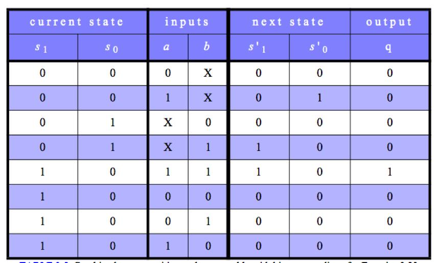
30 Deriving the state transition diagram from a schematic A reverse process of FSM design. q Examine circuit, stating inputs, outputs, and state bits. q Write next state and output equations. q Create next state and output tables. q Reduce the next state table to eliminate unreachable states. q Assign each valid state bit combination a name. q Rewrite next state and output tables with state names. q Draw state transition diagram. q State Digital Design in words and Computer what Architecture: the ARM FSM Edition does Chapter 3 <82> 82

31 The input is A 1:0 and the output is Unlock. The state bits are already labeled. This is a Moore machine because the output depends only on the state bits. Write down the next state and output equations directly: Chapter 3 <83> 83


32 writes down the next state and output tables from the equations. Chapter 3 <84> 84

33 Remove unused states and combine rows using don t cares. The S 1:0 = 11 state is never listed as a possible next state, so rows with this current state are removed. For current state S 1:0 = 10, the next state is always S 1:0 = 00, independent of the inputs, so don t cares are inserted for the inputs. Assign names to each state bit combination: S0 is S 1:0 = 00, S1 is S 1:0 = 01, and S2 is S 1:0 = 10. Chapter 3 <85> 85

34 Chapter 3 <86> 86
35 More Examples Problem 1. Analyze the following FSM. Write down the state transition and output tables, and sketch the state transition diagram. The output is Y. You should use binary state encoding, and list all possible states in your state transition table and diagram. Then, you should remove redundant states, and derive a simplified state table and diagram. 87
36 Problem 2. Output Y Analyze the following FSM that consists of two T flip flops and two AND gates. Write down the state transition and output tables, and sketch the state transition diagram. Note that this problem uses a T flip-flop instead of a D flip-flop in the FSM. 88
37 Problem 3. Design an FSM with one input A and one output Y. Y should be 1 if A has been 1 during at least three most recent consecutive clock cycles. Show your state transition diagram, encoded state transition table (you should use binary encoding), and the next state and output Boolean equations if you use D flip-flops in your FSM (as we usually do in Chapter 3 of the textbook). Problem 4. Redo the previous problem assume that you use J-K flip-flops in your FSM, instead of D flip-flops. Note that if you need two J-K flip-flops A and B, then you need to write down Boolean equations for J A, K A, J B, and K B. 89
38 Exercise Analyze the FSM shown below. Write the state transition and output tables and sketch the state transition diagram. Describe in words what the FSM does. 2-<90>
39 Textbook exercise <91>
40 Problem. Provide the Q output signal using a J-K flip-flop, which has an active low Set and an active low Reset and they are asynchronous. The asynchronous inputs take precedence over the synchronous inputs. Assume that propagation delays are negligent Chapter 3 <92> 92
41 Factoring State Machines Break a complex FSM into smaller interacting FSMs outputs of some machines are the inputs of some other machines Example: Modify traffic light controller to have Parade Mode. Two more inputs: P, R When assert P, i.e., P = 1, for at least one cycle, enter Parade Mode & Bravado Blvd light stays green. Once put into parade mode, controller proceeds through its usual sequence till L B turns green, then remains in that state with L B green until parade mode ends. When asserting R, i.e., R = 1, for at least one cycle, leave Parade Mode. Chapter 3 <93>
42 Parade FSM Step 1: Unfactored FSM P R T A T B Controller FSM L A L B Step 2: Factored FSM P R Mode FSM M Mode FSM asserts M when in parade mode. T A T B Lights FSM L A L B Controller FSM Chapter 3 <94>
43 Factored FSM Reset S0 L A : green L B : red T A TA S1 L A : yellow L B : red S3 L A : red L B : yellow MT B S2 L A : red L B : green Reset S0 M: 0 P P R S1 M: 1 M + T B R Lights FSM Mode FSM Chapter 3 <95>
44 Unfactored FSM S0, S1, S2, S3 handle normal mode. S4, S5, S6, S7 handle parade mode. Chapter 3 <96>
45 Compare Reset T A TA S0 L A : green L B : red S1 L A : yellow L B : red S3 L A : red L B : yellow MT B S2 L A : red L B : green Reset S0 M: 0 P P R S1 M: 1 M + T B Lights FSM Mode FSM R Reset T A TA S0 L A : green L B : red S1 L A : yellow L B : red original FSM S3 L A : red L B : yellow S2 L A : red L B : green T B Chapter 3 <97> T B
Finite State Machine (FSM)
") Finite State Machine (FSM) Consists of: State register Stores current state Loads next state at clock edge Combinational logic Computes the next state Computes the outputs S S Next State CLK Current State
Finite State Machine (FSM) Consists of: State register Stores current state Loads next state at clock edge Combinational logic Computes the next state Computes the outputs S S Next State CLK Current State
Synchronous Sequential Circuit Design. Digital Computer Design
 Synchronous Sequential Circuit Design Digital Computer Design Races and Instability Combinational logic has no cyclic paths and no races If inputs are applied to combinational logic, the outputs will always
Chapter 3. Digital Design and Computer Architecture, 2 nd Edition. David Money Harris and Sarah L. Harris. Chapter 3 <1>
 Chapter 3 Digital Design and Computer Architecture, 2 nd Edition David Money Harris and Sarah L. Harris Chapter 3 Chapter 3 :: Topics Introduction Latches and Flip-Flops Synchronous Logic Design Finite
Synchronous Sequential Logic
 1 IT 201 DIGITAL SYSTEMS DESIGN MODULE4 NOTES Synchronous Sequential Logic Sequential Circuits - A sequential circuit consists of a combinational circuit and a feedback through the storage elements in
Chapter 3. Chapter 3 :: Topics. Introduction. Sequential Circuits
 Chapter 3 Chapter 3 :: Topics igital esign and Computer Architecture, 2 nd Edition avid Money Harris and Sarah L. Harris Introduction Latches and Flip Flops Synchronous Logic esign Finite State Machines
CPE100: Digital Logic Design I
 Chapter 3 Professor Brendan Morris, SEB 3216, brendan.morris@unlv.edu http://www.ee.unlv.edu/~b1morris/cpe1/ CPE1: Digital Logic Design I Section 14: Dr. Morris Sequential Logic Design Chapter 3 Chapter
ECEN 248: INTRODUCTION TO DIGITAL SYSTEMS DESIGN. Week 7 Dr. Srinivas Shakkottai Dept. of Electrical and Computer Engineering
 ECEN 248: INTRODUCTION TO DIGITAL SYSTEMS DESIGN Week 7 Dr. Srinivas Shakkottai Dept. of Electrical and Computer Engineering SEQUENTIAL CIRCUITS: LATCHES Overview Circuits require memory to store intermediate
Week-5. Sequential Circuit Design. Acknowledgement: Most of the following slides are adapted from Prof. Kale's slides at UIUC, USA.
 Week-5 Sequential Circuit Design Acknowledgement: Most of the following slides are adapted from Prof. Kale's slides at UIUC, USA. Storing a value: SR = 00 What if S = 0 and R = 0? The equations on the
Ch 7. Finite State Machines. VII - Finite State Machines Contemporary Logic Design 1
 Ch 7. Finite State Machines VII - Finite State Machines Contemporary Logic esign 1 Finite State Machines Sequential circuits primitive sequential elements combinational logic Models for representing sequential
CprE 281: Digital Logic
 CprE 281: Digital Logic Instructor: Alexander Stoytchev http://www.ece.iastate.edu/~alexs/classes/ Synchronous Sequential Circuits Basic Design Steps CprE 281: Digital Logic Iowa State University, Ames,
CPE100: Digital Logic Design I
 Professor Brendan Morris, SEB 3216, brendan.morris@unlv.edu CPE100: Digital Logic Design I Midterm02 Review http://www.ee.unlv.edu/~b1morris/cpe100/ 2 Logistics Thursday Nov. 16 th In normal lecture (13:00-14:15)
Models for representing sequential circuits
 Sequential Circuits Models for representing sequential circuits Finite-state machines (Moore and Mealy) Representation of memory (states) Changes in state (transitions) Design procedure State diagrams
Synchronous Sequential Circuit Design. Dr. Ehab A. H. AL-Hialy Page 1
 Synchronous Sequential Circuit Design Dr. Ehab A. H. AL-Hialy Page Motivation Analysis of a few simple circuits Generalizes to Synchronous Sequential Circuits (SSC) Outputs are Function of State (and Inputs)
UNIVERSITY OF BOLTON SCHOOL OF ENGINEERING BENG (HONS) ELECTRICAL & ELECTRONICS ENGINEERING EXAMINATION SEMESTER /2017
 ELECTRICAL & ELECTRONICS ENGINEERING EXAMINATION SEMESTER /2017") UNIVERSITY OF BOLTON TW35 SCHOOL OF ENGINEERING BENG (HONS) ELECTRICAL & ELECTRONICS ENGINEERING EXAMINATION SEMESTER 2-2016/2017 INTERMEDIATE DIGITAL ELECTRONICS AND COMMUNICATIONS MODULE NO: EEE5002
UNIVERSITY OF BOLTON TW35 SCHOOL OF ENGINEERING BENG (HONS) ELECTRICAL & ELECTRONICS ENGINEERING EXAMINATION SEMESTER 2-2016/2017 INTERMEDIATE DIGITAL ELECTRONICS AND COMMUNICATIONS MODULE NO: EEE5002
CPE100: Digital Logic Design I
 Professor Brendan Morris, SEB 3216, brendan.morris@unlv.edu CPE100: Digital Logic Design I Final Review http://www.ee.unlv.edu/~b1morris/cpe100/ 2 Logistics Tuesday Dec 12 th 13:00-15:00 (1-3pm) 2 hour
Sequential Circuit Design
 Sequential Circuit esign esign Procedure. Specification 2. Formulation Obtain a state diagram or state table 3. State Assignment Assign binary codes to the states 4. Flip-Flop Input Equation etermination
Digital Logic and Design (Course Code: EE222) Lecture 19: Sequential Circuits Contd..
 Lecture 19: Sequential Circuits Contd..") Indian Institute of Technology Jodhpur, Year 2017-2018 Digital Logic and Design (Course Code: EE222) Lecture 19: Sequential Circuits Contd.. Course Instructor: Shree Prakash Tiwari Email: sptiwari@iitj.ac.in
Indian Institute of Technology Jodhpur, Year 2017-2018 Digital Logic and Design (Course Code: EE222) Lecture 19: Sequential Circuits Contd.. Course Instructor: Shree Prakash Tiwari Email: sptiwari@iitj.ac.in
EECS Components and Design Techniques for Digital Systems. FSMs 9/11/2007
 EECS 150 - Components and Design Techniques for Digital Systems FSMs 9/11/2007 Sarah Bird Electrical Engineering and Computer Sciences University of California, Berkeley Slides borrowed from David Culler
The Design Procedure. Output Equation Determination - Derive output equations from the state table
 The Design Procedure Specification Formulation - Obtain a state diagram or state table State Assignment - Assign binary codes to the states Flip-Flop Input Equation Determination - Select flipflop types
Synchronous Sequential Circuit Design
 Synchronous Sequential Circuit Design 1 Sequential circuit design In sequential circuit design, we turn some description into a working circuit We first make a state table or diagram to express the computation
Lecture 17: Designing Sequential Systems Using Flip Flops
 EE210: Switching Systems Lecture 17: Designing Sequential Systems Using Flip Flops Prof. YingLi Tian April 11, 2019 Department of Electrical Engineering The City College of New York The City University
COE 202: Digital Logic Design Sequential Circuits Part 3. Dr. Ahmad Almulhem ahmadsm AT kfupm Phone: Office:
 COE 202: Digital Logic Design Sequential Circuits Part 3 Dr. Ahmad Almulhem Email: ahmadsm AT kfupm Phone: 860-7554 Office: 22-324 Objectives Important Design Concepts State Reduction and Assignment Design
ENGG 1203 Tutorial _03 Laboratory 3 Build a ball counter. Lab 3. Lab 3 Gate Timing. Lab 3 Steps in designing a State Machine. Timing diagram of a DFF
 ENGG 1203 Tutorial _03 Laboratory 3 Build a ball counter Timing diagram of a DFF Lab 3 Gate Timing difference timing for difference kind of gate, cost dependence (1) Setup Time = t2-t1 (2) Propagation
COE 202: Digital Logic Design Sequential Circuits Part 3. Dr. Ahmad Almulhem ahmadsm AT kfupm Phone: Office:
 COE 202: Digital Logic Design Sequential Circuits Part 3 Dr. Ahmad Almulhem Email: ahmadsm AT kfupm Phone: 860-7554 Office: 22-324 Objectives State Reduction and Assignment Design of Synchronous Sequential
Sequential Synchronous Circuit Analysis
 Sequential Synchronous Circuit Analysis General Model Current State at time (t) is stored in an array of flip-flops. Next State at time (t+1) is a Boolean function of State and Inputs. Outputs at time
Sequential Logic. Rab Nawaz Khan Jadoon DCS. Lecturer COMSATS Lahore Pakistan. Department of Computer Science
 Sequential Logic Rab Nawaz Khan Jadoon DCS COMSATS Institute of Information Technology Lecturer COMSATS Lahore Pakistan Digital Logic and Computer Design Sequential Logic Combinational circuits with memory
ELCT201: DIGITAL LOGIC DESIGN
 ELCT201: DIGITAL LOGIC DESIGN Dr. Eng. Haitham Omran, haitham.omran@guc.edu.eg Dr. Eng. Wassim Alexan, wassim.joseph@guc.edu.eg Lecture 6 Following the slides of Dr. Ahmed H. Madian محرم 1439 ه Winter
Chapter 4 Part 2 Sequential Circuits
 University of Wisconsin - Madison ECE/Comp Sci 352 Digital Systems Fundamentals Kewal K. Saluja and Yu Hen Hu Spring 2002 Chapter 4 Part 2 Sequential Circuits Originals by: Charles R. Kime and Tom Kamisnski
ELEC Digital Logic Circuits Fall 2014 Sequential Circuits (Chapter 6) Finite State Machines (Ch. 7-10)
 Finite State Machines (Ch. 7-10)") ELEC 2200-002 Digital Logic Circuits Fall 2014 Sequential Circuits (Chapter 6) Finite State Machines (Ch. 7-10) Vishwani D. Agrawal James J. Danaher Professor Department of Electrical and Computer Engineering
ELEC 2200-002 Digital Logic Circuits Fall 2014 Sequential Circuits (Chapter 6) Finite State Machines (Ch. 7-10) Vishwani D. Agrawal James J. Danaher Professor Department of Electrical and Computer Engineering
Synchronous Sequential Logic Part I. BME208 Logic Circuits Yalçın İŞLER
 Synchronous Sequential Logic Part I BME28 Logic Circuits Yalçın İŞLER islerya@yahoo.com http://me.islerya.com Sequential Logic Digital circuits we have learned, so far, have been combinational no memory,
CS221: Digital Design. Dr. A. Sahu. Indian Institute of Technology Guwahati
 CS221: Digital Design Counter&Registers Dr. A. Sahu DeptofComp.Sc.&Engg. Indian Institute of Technology Guwahati Outline Counter : Synchronous Vs Asynchronous Counter: Finite it State t Machine Mhi A register
King Fahd University of Petroleum and Minerals College of Computer Science and Engineering Computer Engineering Department
 King Fahd University of Petroleum and Minerals College of Computer Science and Engineering Computer Engineering Department Page 1 of 13 COE 202: Digital Logic Design (3-0-3) Term 112 (Spring 2012) Final
COEN 312 DIGITAL SYSTEMS DESIGN - LECTURE NOTES Concordia University
 1 OEN 312 DIGIAL SYSEMS DESIGN - LEURE NOES oncordia University hapter 6: Registers and ounters NOE: For more examples and detailed description of the material in the lecture notes, please refer to the
Sequential Circuit Analysis
 Sequential Circuit Analysis Last time we started talking about latches and flip-flops, which are basic one-bit memory units. Today we ll talk about sequential circuit analysis and design. First, we ll
15.1 Elimination of Redundant States
 15.1 Elimination of Redundant States In Ch. 14 we tried not to have unnecessary states What if we have extra states in the state graph/table? Complete the table then eliminate the redundant states Chapter
ELE2120 Digital Circuits and Systems. Tutorial Note 9
 ELE2120 Digital Circuits and Systems Tutorial Note 9 Outline 1. Exercise(1) Sequential Circuit Analysis 2. Exercise (2) Sequential Circuit Analysis 3. Exercise (3) Sequential Circuit Analysis 4. Ref. Construction
Sequential vs. Combinational
 Sequential Circuits Sequential vs. Combinational Combinational Logic: Output depends only on current input TV channel selector (-9) inputs system outputs Sequential Logic: Output depends not only on current
Synchronous Sequential Logic Part I
 Synchronous Sequential Logic Part I Mantıksal Tasarım BBM23 section instructor: Ufuk Çelikcan Sequential Logic Digital circuits we have learned, so far, have been combinational no memory, outputs are entirely
Problem Set 9 Solutions
 CSE 26 Digital Computers: Organization and Logical Design - 27 Jon Turner Problem Set 9 Solutions. For each of the sequential circuits shown below, draw in the missing parts of the timing diagrams. You
EE40 Lec 15. Logic Synthesis and Sequential Logic Circuits
 EE40 Lec 15 Logic Synthesis and Sequential Logic Circuits Prof. Nathan Cheung 10/20/2009 Reading: Hambley Chapters 7.4-7.6 Karnaugh Maps: Read following before reading textbook http://www.facstaff.bucknell.edu/mastascu/elessonshtml/logic/logic3.html
Digital Circuits ECS 371
 Digital Circuits ECS 371 Dr. Prapun Suksompong prapun@siit.tu.ac.th Lecture 18 Office Hours: BKD 3601-7 Monday 9:00-10:30, 1:30-3:30 Tuesday 10:30-11:30 1 Announcement Reading Assignment: Chapter 7: 7-1,
ELCT201: DIGITAL LOGIC DESIGN
 ELCT201: DIGITAL LOGIC DESIGN Dr. Eng. Haitham Omran, haitham.omran@guc.edu.eg Dr. Eng. Wassim Alexan, wassim.joseph@guc.edu.eg Following the slides of Dr. Ahmed H. Madian Lecture 10 محرم 1439 ه Winter
Lecture 14: State Tables, Diagrams, Latches, and Flip Flop
 EE210: Switching Systems Lecture 14: State Tables, Diagrams, Latches, and Flip Flop Prof. YingLi Tian Nov. 6, 2017 Department of Electrical Engineering The City College of New York The City University
EEE2135 Digital Logic Design
 EEE2135 Digital Logic Design Chapter 7. Sequential Circuits Design 서강대학교 전자공학과 1. Model of Sequential Circuits 1) Sequential vs. Combinational Circuits a. Sequential circuits: Outputs depend on both the
Synchronous Sequential Circuit
 Synchronous Sequential Circuit The change of internal state occurs in response to the synchronized clock pulses. Data are read during the clock pulse (e.g. rising-edge triggered) It is supposed to wait
Digital Electronics Sequential Logic
 /5/27 igital Electronics Sequential Logic r. I. J. Wassell Sequential Logic The logic circuits discussed previously are known as combinational, in that the output depends only on the condition of the latest
Digital Logic Design - Chapter 5
 Digital Logic Design - Chapter 5 S. Design a 2-bit binary up counter a) using positive-edge-triggered D flip-flops. b) using positive-edge-triggered T flip-flops. c) using positive-edge-triggered JK flip-flops.
Chapter 6 Introduction to state machines
 9..7 hapter 6 Introduction to state machines Dr.-Ing. Stefan Werner Table of content hapter : Switching Algebra hapter : Logical Levels, Timing & Delays hapter 3: Karnaugh-Veitch-Maps hapter 4: ombinational
Finite State Machine. By : Ali Mustafa
 Finite State Machine By : Ali Mustafa So Far We have covered the memory elements issue and we are ready to implement the sequential circuits. We need to know how to Deal(analyze) with a sequential circuit?
Sequential Circuits Sequential circuits combinational circuits state gate delay
 Sequential Circuits Sequential circuits are those with memory, also called feedback. In this, they differ from combinational circuits, which have no memory. The stable output of a combinational circuit
Sequential logic and design
 Principles Of Digital Design Sequential logic and design Analysis State-based (Moore) Input-based (Mealy) FSM definition Synthesis State minimization Encoding Optimization and timing Copyright 20-20by
Appendix B. Review of Digital Logic. Baback Izadi Division of Engineering Programs
 Appendix B Review of Digital Logic Baback Izadi Division of Engineering Programs bai@engr.newpaltz.edu Elect. & Comp. Eng. 2 DeMorgan Symbols NAND (A.B) = A +B NOR (A+B) = A.B AND A.B = A.B = (A +B ) OR
3. Complete the following table of equivalent values. Use binary numbers with a sign bit and 7 bits for the value
 EGC22 Digital Logic Fundamental Additional Practice Problems. Complete the following table of equivalent values. Binary. Octal 35.77 33.23.875 29.99 27 9 64 Hexadecimal B.3 D.FD B.4C 2. Calculate the following
Fundamentals of Computer Systems
 Fundamentals of Computer Systems Review for the Midterm Stephen A. Edwards Columbia University Spring 22 The Midterm 75 minutes 4 5 problems Closed book Simple calculators are OK, but unnecessary One double-sided
Lecture (08) Synchronous Sequential Logic
 Synchronous Sequential Logic") Lecture (08) Synchronous Sequential Logic By: Dr. Ahmed ElShafee ١ Dr. Ahmed ElShafee, ACU : Spring 2018, CSE303 Logic design II Analysis of Clocked Sequential Circuits The behavior of a clocked sequential
Lecture (08) Synchronous Sequential Logic By: Dr. Ahmed ElShafee ١ Dr. Ahmed ElShafee, ACU : Spring 2018, CSE303 Logic design II Analysis of Clocked Sequential Circuits The behavior of a clocked sequential
State Machines ELCTEC-131
 State Machines ELCTEC-131 Switch Debouncer A digital circuit that is used to remove the mechanical bounce from a switch contact. When a switch is closed, the contacts bounce from open to closed to cause
14.1. Unit 14. State Machine Design
 4. Unit 4 State Machine Design 4.2 Outcomes I can create a state diagram to solve a sequential problem I can implement a working state machine given a state diagram STATE MACHINES OVERVIEW 4.3 4.4 Review
Fundamentals of Computer Systems
 Fundamentals of Computer Systems Review for the Final Stephen A. Edwards Columbia University Summer 25 The Final 2 hours 8 problems Closed book Simple calculators are OK, but unnecessary One double-sided
Synchronous Sequential Logic. Chapter 5
 Synchronous Sequential Logic Chapter 5 Other Flip Flops D flip flops requires smallest number of gates. Thus, they are commonly used Other flip flops are JK flip flops T flip flops
Final Exam. ECE 25, Spring 2008 Thursday, June 12, Problem Points Score Total 90
 Final Exam ECE 25, Spring 2008 Thursday, June 12, 2008 Name: PID: Problem Points Score 1 10 2 10 3 10 4 10 5 10 6 10 7 10 8 10 9 10 Total 90 1) Number representation (10 pts) a) For each binary vector
EE 209 Logic Cumulative Exam Name:
 EE 209 Logic Cumulative Exam Name: 1.) Answer the following questions as True or False a.) A 4-to-1 multiplexer requires at least 4 select lines: true / false b.) An 8-to-1 mux and no other logi can be
Lecture 10: Synchronous Sequential Circuits Design
 Lecture 0: Synchronous Sequential Circuits Design. General Form Input Combinational Flip-flops Combinational Output Circuit Circuit Clock.. Moore type has outputs dependent only on the state, e.g. ripple
Mealy & Moore Machines
 Mealy & Moore Machines Moore Machine is a finite-state machine whose output values are determined solely by its current state and can be defined as six elements (S, S 0, Σ, Λ, T, G), consisting of the
Digital Design. Sequential Logic
 Principles Of igital esign Chapter 6 Sequential Logic Chapter preview Boolean algebra 3 Logic gates and flip-flops 3 Finite-state machine 6 Logic design techniques 4 Sequential design techniques 6 Binary
University of Minnesota Department of Electrical and Computer Engineering
 University of Minnesota Department of Electrical and Computer Engineering EE2301 Fall 2008 Introduction to Digital System Design L. L. Kinney Final Eam (Closed Book) Solutions Please enter your name, ID
EET 310 Flip-Flops 11/17/2011 1
 EET 310 Flip-Flops 11/17/2011 1 FF s and some Definitions Clock Input: FF s are controlled by a trigger or Clock signal. All FF s have a clock input. If a device which attempts to do a FF s task does not
Fundamentals of Digital Design
 Fundamentals of Digital Design Digital Radiation Measurement and Spectroscopy NE/RHP 537 1 Binary Number System The binary numeral system, or base-2 number system, is a numeral system that represents numeric
EGR224 F 18 Assignment #4
 EGR224 F 18 Assignment #4 ------------------------------------------------------------------------------------------------------------- Due Date: Friday (Section 10), October 19, by 5 pm (slide it under
Latches. October 13, 2003 Latches 1
 Latches The second part of CS231 focuses on sequential circuits, where we add memory to the hardware that we ve already seen. Our schedule will be very similar to before: We first show how primitive memory
Written reexam with solutions for IE1204/5 Digital Design Monday 14/
 Written reexam with solutions for IE204/5 Digital Design Monday 4/3 206 4.-8. General Information Examiner: Ingo Sander. Teacher: William Sandqvist phone 08-7904487 Exam text does not have to be returned
Parity Checker Example. EECS150 - Digital Design Lecture 9 - Finite State Machines 1. Formal Design Process. Formal Design Process
 Parity Checker Example A string of bits has even parity if the number of 1 s in the string is even. Design a circuit that accepts a bit-serial stream of bits and outputs a 0 if the parity thus far is even
Clocked Synchronous State-machine Analysis
 Clocked Synchronous State-machine Analysis Given the circuit diagram of a state machine: Analyze the combinational logic to determine flip-flop input (excitation) equations: D i = F i (Q, inputs) The input
Department of Electrical & Electronics EE-333 DIGITAL SYSTEMS
 Department of Electrical & Electronics EE-333 DIGITAL SYSTEMS 1) Given the two binary numbers X = 1010100 and Y = 1000011, perform the subtraction (a) X -Y and (b) Y - X using 2's complements. a) X = 1010100
Lecture 3 Review on Digital Logic (Part 2)
") Lecture 3 Review on Digital Logic (Part 2) Xuan Silvia Zhang Washington University in St. Louis http://classes.engineering.wustl.edu/ese461/ ircuit Optimization Simplest implementation ost criterion literal
Lecture 3 Review on Digital Logic (Part 2) Xuan Silvia Zhang Washington University in St. Louis http://classes.engineering.wustl.edu/ese461/ ircuit Optimization Simplest implementation ost criterion literal
LOGIC CIRCUITS. Basic Experiment and Design of Electronics
 Basic Experiment and Design of Electronics LOGIC CIRCUITS Ho Kyung Kim, Ph.D. hokyung@pusan.ac.kr School of Mechanical Engineering Pusan National University Outline Combinational logic circuits Output
ECE 341. Lecture # 3
 ECE 341 Lecture # 3 Instructor: Zeshan Chishti zeshan@ece.pdx.edu October 7, 2013 Portland State University Lecture Topics Counters Finite State Machines Decoders Multiplexers Reference: Appendix A of
Counters. We ll look at different kinds of counters and discuss how to build them
 Counters We ll look at different kinds of counters and discuss how to build them These are not only examples of sequential analysis and design, but also real devices used in larger circuits 1 Introducing
BER KELEY D AV IS IR VINE LOS AN GELES RIVERS IDE SAN D IEGO S AN FRANCISCO
 UN IVERSIT Y O F CA LIFO RNI A AT BERKELEY BER KELEY D AV IS IR VINE LOS AN GELES RIVERS IDE SAN D IEGO S AN FRANCISCO SAN TA BARBA RA S AN TA CRUZ De p a r tm en t of Ele ctr i ca l En gin e e rin g a
Simplify the following Boolean expressions and minimize the number of literals:
 Boolean Algebra Task 1 Simplify the following Boolean expressions and minimize the number of literals: 1.1 1.2 1.3 Task 2 Convert the following expressions into sum of products and product of sums: 2.1
Overview of Chapter 4
 Overview of hapter 4 Types of Sequential ircuits Storage Elements Latches Flip-Flops Sequential ircuit Analysis State Tables State Diagrams Sequential ircuit Design Specification Assignment of State odes
Sequential Logic Circuits
 Chapter 4 Sequential Logic Circuits 4 1 The defining characteristic of a combinational circuit is that its output depends only on the current inputs applied to the circuit. The output of a sequential circuit,
Chapter 7 Sequential Logic
 Chapter 7 Sequential Logic SKEE2263 Digital Systems Mun im/ismahani/izam {munim@utm.my,e-izam@utm.my,ismahani@fke.utm.my} March 28, 2016 Table of Contents 1 Intro 2 Bistable Circuits 3 FF Characteristics
EECS150 - Digital Design Lecture 23 - FSMs & Counters
 EECS150 - Digital Design Lecture 23 - FSMs & Counters April 8, 2010 John Wawrzynek Spring 2010 EECS150 - Lec22-counters Page 1 One-hot encoding of states. One FF per state. State Encoding Why one-hot encoding?
Chapter 14 Sequential logic, Latches and Flip-Flops
 Chapter 14 Sequential logic, Latches and Flip-Flops Flops Lesson 4 JK Flip Flop Ch14L4-"Digital Principles and Design", Raj Kamal, Pearson Education, 2006 2 JK Flip-Flop ve edge triggered Output Q and
Chapter 5 Synchronous Sequential Logic
 Chapter 5 Synchronous Sequential Logic Sequential circuit: A circuit that includes memory elements. In this case the output depends not only on the current input but also on the past inputs. Memory A synchronous
Lecture 7: Logic design. Combinational logic circuits
 /24/28 Lecture 7: Logic design Binary digital circuits: Two voltage levels: and (ground and supply voltage) Built from transistors used as on/off switches Analog circuits not very suitable for generic
State Graphs FSMs. Page 1
 State Graphs FSMs Page 1 Binary Counter State Graph 00 Q1 Q0 N1 N0 0 0 0 1 0 1 1 0 1 0 1 1 1 1 0 0 11 01 State graphs are graphical representations of TT s They contain the same information: no more, no
Digital Control of Electric Drives
 Digital Control of Electric Drives Logic Circuits - equential Description Form, Finite tate Machine (FM) Czech Technical University in Prague Faculty of Electrical Engineering Ver.. J. Zdenek 27 Logic
I. Motivation & Examples
 I. Motivation & Examples Output depends on current input and past history of inputs. State embodies all the information about the past needed to predict current output based on current input. State variables,
State & Finite State Machines
 State & Finite State Machines Hakim Weatherspoon CS 3410, Spring 2012 Computer Science Cornell University See P&H Appendix C.7. C.8, C.10, C.11 Stateful Components Until now is combinatorial logic Output
Homework #4. CSE 140 Summer Session Instructor: Mohsen Imani. Only a subset of questions will be graded
 Homework #4 CSE 140 Summer Session 2 2017 Instructor: Mohsen Imani Only a subset of questions will be graded 1) For the circuit shown below, do the following: a. Write a logic equation for the output P
ECEN 248: INTRODUCTION TO DIGITAL SYSTEMS DESIGN. Week 9 Dr. Srinivas Shakkottai Dept. of Electrical and Computer Engineering
 ECEN 248: INTRODUCTION TO DIGITAL SYSTEMS DESIGN Week 9 Dr. Srinivas Shakkottai Dept. of Electrical and Computer Engineering TIMING ANALYSIS Overview Circuits do not respond instantaneously to input changes
Analysis of Clocked Sequential Circuits
 Objectives Analysis of Clocked Sequential Circuits The objectives of this lesson are as follows: Analysis of clocked sequential circuits with an example State Reduction with an example State assignment
ASYNCHRONOUS SEQUENTIAL CIRCUITS
 ASYNCHRONOUS SEQUENTIAL CIRCUITS Sequential circuits that are not snchronized b a clock Asnchronous circuits Analsis of Asnchronous circuits Snthesis of Asnchronous circuits Hazards that cause incorrect
Lecture 14 Finite state machines
 Lecture 14 Finite state machines Finite state machines are the foundation of nearly all digital computation. The state diagram captures the desired system behavior A formulaic process turns this diagram
CHW 261: Logic Design
 CHW 26: Logic Design Instructors: Prof. Hala Zayed Dr. Ahmed Shalaby http://www.bu.edu.eg/staff/halazayed4 http://bu.edu.eg/staff/ahmedshalaby4# Slide Digital Fundamentals CHAPTER 8 Counters Slide 2 Counting
6. Finite State Machines
 6. Finite State Machines 6.4x Computation Structures Part Digital Circuits Copyright 25 MIT EECS 6.4 Computation Structures L6: Finite State Machines, Slide # Our New Machine Clock State Registers k Current
ELE2120 Digital Circuits and Systems. Tutorial Note 10
 ELE2120 Digital Circuits and Systems Tutorial Note 10 Outline 1. 1. Sequential Circuit Design 2. 2. Design procedure: a complete example illustration Sequential circuit analysis & design In sequential
11.1 As mentioned in Experiment 10, sequential logic circuits are a type of logic circuit where the output of
 EE 2449 Experiment 11 Jack Levine and Nancy Warter-Perez CALIFORNIA STATE UNIVERSITY LOS ANGELES Department of Electrical and Computer Engineering EE-2449 Digital Logic Lab EXPERIMENT 11 SEQUENTIAL CIRCUITS
Chapter 4. Sequential Logic Circuits
 Chapter 4 Sequential Logic Circuits 1 2 Chapter 4 4 1 The defining characteristic of a combinational circuit is that its output depends only on the current inputs applied to the circuit. The output of