DDR4 Board Design and Signal Integrity Verification Challenges
|
|
|
- Roy Webb
- 5 years ago
- Views:
Transcription


1 DDR4 Board Design and Signal Integrity Verification Challenges
2 Outline Enabling DDR4 Pseudo Open Drain Driver - Benefit POD SI effects VrefDQ Calculation Data Eye Simulating SSN
3 New Drive Standards Difference DDR4 (Pseudo Open Drain) DDR3 (Stub Series Terminated Logic)
4 Current still flows when driving low New Drive Standards Why? DDR4 DDR3


5 New Drive Standards Why? No current draw when driving a high DDR4 DDR3
6 Power Savings with DBI Ensure more 1 s than 0 s with POD If more than 4 bits in a byte are 0, toggle bits DBI shared with DM => only one feature enabled DBI pin is I/O (effects both reads and writes)
7 Implications for SI What does asymmetric termination mean for reference threshold voltage ( center voltage of eye )? Take average voltage of high and low at receiver Assume a very short trace for sake of simple calculations Assume balanced high and low drive strength Rt = Termination Resistance Zo = Transmission Line Impedance Zd = Driver Output Impedance
8 DDR3 Center Voltage When Driving High When Driving Low
9 DDR4 Center Voltage When Driving High When Driving Low
10 DDR3, Vcent = Vdd/2 DDR3 vs. DDR4 Vcent Comparison Constant, regardless of setup DDR4, Vcent = f(rt, Zd) Varies from setup to setup Varies from read to write Varies across access to different DRAMs


11 Input Threshold Levels DDR3 Absolute Vinh/vinl thresholds stayed constant in DDR3 across designs DDR4 Absolute Vih/Vil threshold levels can change in DDR4

12 Simple Comparison Controller 50 Ohm Transmission Line DRAM Vary DRAM s ODT to see center level of eye 2400Mbps Datarate

13 DDR3 Sweeping Rx ODT No change in Center of eye with ODT

14 DDR4 Eye Shifting Eye center shifts with ODT change
15 Vref for a Device Need Precision programmable reference voltage Center voltage can vary across pins Individual Vref per pin may be too expensive Silicon and power How to determine voltage used for all pins?
16 Determining Vref Avg 8 bit device, one Vref resource Eye-center of bits different, as below 800mV 750mV 730mV 725mV 720mV 710mV 705mV 700mV
17 Determining Vref Margin Loss Margin Loss for a given bit V d = Vref(device) V x = Vref(pin_x) Margin Loss = M p M d = V d V x Note: (The margin loss will be negative on the low side waveform in this case i.e. a margin gain) 17
18 Average Margin Loss Option 1 Margin Loss = M p M d = V d V x V d = V x. (Device Vref is average of all pins) n (V d V x ) Average Margin Loss = = V d n V x n = nv d n V d = 0 As intuitively expected! n
19 Average Margin Loss Option 2 Average Margin Loss = = V d V max + V d V min n Margin Loss = M p M d = V d V x V d = V max+v min. (Device Vref is average of extreme pins) 2 (V d V x ) n + x max,min (V d V x ) n = 2V d n V max + V min n + x max,min n V d V x = 2 n V max + V min 2 V max + V min n + x max,min n V d V x = x max,min (V d V x ) n
20 Average Margin Loss Comparison Option 1 always has average margin loss of 0 Option 2 has average margin loss (on one side) of 0 Shouldn t we choose Option 1? No! Consider worst case pins.
 730-68 = 662mV (Vinl) 750mV 750+68 = 818mV (Vinh) 750-68 =")
21 Average Margin Loss Comparison Option 1: Average of all signals Option 2: Average of extreme signals 730mV = 798mV (Vinh) = 662mV (Vinl) 750mV = 818mV (Vinh) = 682mV (Vinl)
22 Average Margin Loss Comparison 800mV 750mV 730mV 725mV 720mV 710mV 705mV 700mV Assume eye height same at all pins, Eye height of 260mV (Vcenter +/- 130mV) (Not strictly true, but 800mV is still worst case) 800mV center signal swings between 670mV to 930mV Option = 798mV (Vinh) = 662mV (Vinl) 930mV 800mV mV Option = 818mV (Vinh) = 682mV (Vinl)


23 Average Margin Loss Comparison Do you really want to spread out the margin of your worst case signal to the non-critical signals? Margin Margin If worst case signals work, all other signals will work.

24 Vref for DDR4 DRAM Single Voltage, regardless of x4, x8 or x16 JC-42.3C, Ballot A

25 Vref for DDR4 DRAM Range from 45% of Vdd to 92.5% of Vdd Step size can be between 0.5%Vddq to 0.8%Vddq Exact value will be specific to the DRAM and should be in the datasheet
26 Vref for Controller (Read) Single Vref for entire channel Inexpensive, easy for controller to implement Greater similarity required in DQ signal characteristics
27 Vref for Controller (Read) Single Vref for each DRAM in the rank Allows for grouping of signals going to each DRAM
28 Vref for Controller (Read) Single Vref for each Lane in the rank Allows for grouping of signals going to each Lane Differs from previous setup only for x16 DRAMs
29 Vref for Controller (Read) Single vs. Multi-Rank support Cost vs. layoutability
30 Generating the Eye Concept of Eye borrowed from SerDes No self-clocking, or clock recovery scheme Explicit clock or strobe at play In simulation run, cannot just specify frequency Must incorporate clock/strobe
31 Eye - What the Strobe Sees Double Counted Not Counted

32 Eye Generation - Folding vs. Strobe Data running at 2400MT/s Clock P/N slightly offset to simulate poor trace design.


33 Compare Folding vs. Strobing DQ Eye Sampled at Strobe DQ Eye Wrapped at ps
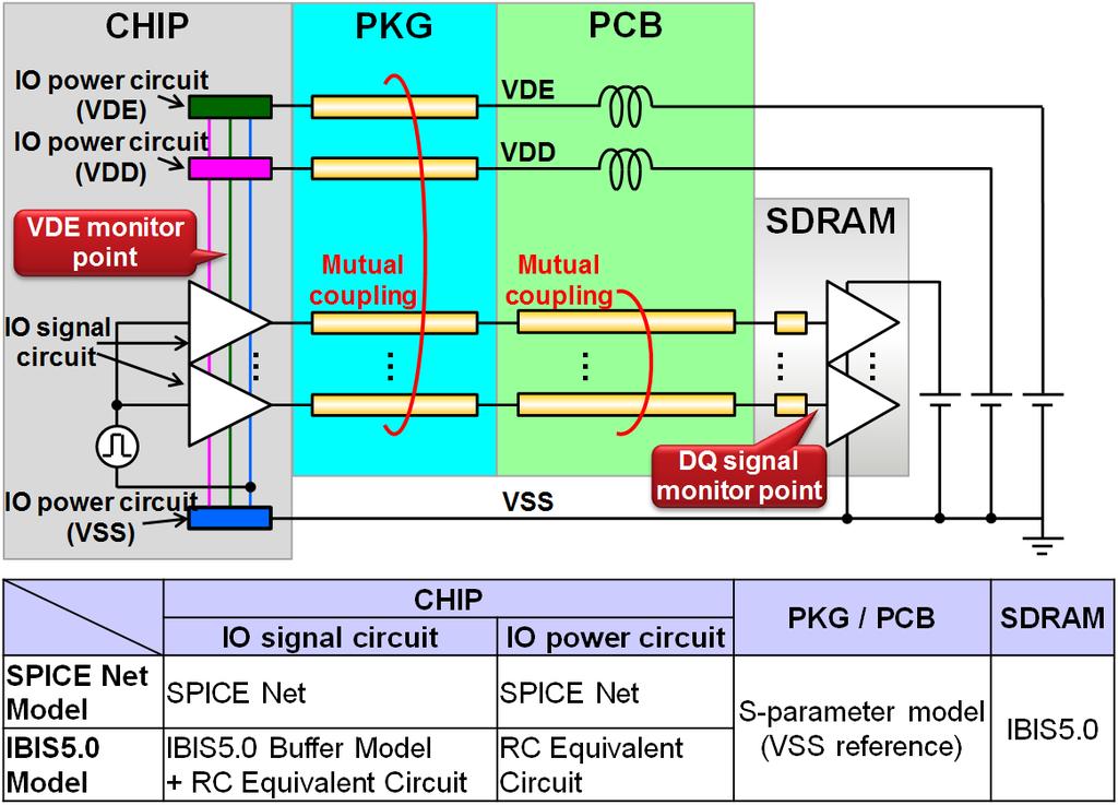
34 Enabling DDR4 Simulation with Power Aware IBIS

35 Simulating SSO is a desired part of system PDN design Choice of I/O model directly relates to simulation time and accuracy of SI and PI results Common choices include Spice, IBIS 4.2 and IBIS 5.0. I/O Modeling Options

36 Simulation Model Trade-offs SPICE Netlist IBIS 4.2 IBIS 5.0 Simulation time SI simulation accuracy PI simulation accuracy Longer Shorter Shorter High High High High Low High

37 Traditional IBIS model algorithms assume max operating frequency related to length of V-T waveforms Length of a half cycle Length of Initial Delay + Length of Active Area Initial Delay cannot be removed in IBIS 5.0 due to pre-driver switching currents IBIS Model Overclocking Concerns

38 Correcting Overclocking in the EDA Software Pre-driver and driver currents must be correctly summed relative to each switching event Must support Length of a half cycle = Length of Active Area

39 Correcting Overclocking in the EDA Software Improved simulation algorithms generate correct results at every valid datarate

40 System Level Simulation

41 Includes Controller, x32 DQ bus, Address/ Command Simulation Schematic
42 Simulation Results Single net simulation Excludes SSO and Crosstalk 2400 Mbps Comparison at SDRAM die pad Eye Widths (TdiVW) within 7ps (1.9%)

43 Simulation includes SSO noise 32 DQs and 4 DQ/DQS# pairs switching 2400 Mbps Simulation Results Comparison of VDE at controller die Comparison of DQ at SDRAM die pad SSO noise simulated accurately
 within 22ps (7.")
44 Simulation Results Simulation includes SSO and Crosstalk 1 DQ as Victim net 31 DQs and 4 DQ/DQS# pairs as Aggressor nets 2400 Mbps Comparison at SDRAM die pad Eye Widths (TdiVW) within 22ps (7.3%) Some mismatch from un-modeled pre-driver delay sensitivity
 98.")
45 EDA software is critical for DDR4 analysis Use of DBI Setting valid Vref levels Rx masks for timing verification Generate data eyes with correct jitter contributions Conclusions IBIS 5.0 power aware models useful for system level analysis Significantly speed up simulation time Reasonable accuracy of SSO jitter effects 60ns simulation duration (one cycle of PRBS7) 98.6% sim time reduction!
AN B. Basic PCB traces transmission line effects causing signal integrity degradation simulation using Altium DXP version 6.
 AN200805-01B Basic PCB traces transmission line effects causing signal integrity degradation simulation using Altium DXP version 6.9 By Denis Lachapelle eng. and Anne Marie Coutu. May 2008 The objective
TITLE. In-depth Analysis of DDR3/DDR4 Channel with Active Termination. Image. Topic: Topic: Changwook Yoon, (Intel)
") TITLE Topic: o Nam elementum commodo mattis. Pellentesque In-depth Analysis of DDR3/DDR4 Channel with Active Termination malesuada blandit euismod. Topic: Changwook Yoon, (Intel) o Nam elementum commodo
TITLE Topic: o Nam elementum commodo mattis. Pellentesque In-depth Analysis of DDR3/DDR4 Channel with Active Termination malesuada blandit euismod. Topic: Changwook Yoon, (Intel) o Nam elementum commodo
IBIS EBD Modeling, Usage and Enhancement An Example of Memory Channel Multi-board Simulation
 IBIS EBD Modeling, Usage and Enhancement An Example of Memory Channel Multi-board Simulation Tao Xu Asian IBIS Summit taoxu@sigrity.com Shanghai China November 11, 2008 Agenda Memory channel simulation
Digital Integrated Circuits A Design Perspective
 Semiconductor Memories Adapted from Chapter 12 of Digital Integrated Circuits A Design Perspective Jan M. Rabaey et al. Copyright 2003 Prentice Hall/Pearson Outline Memory Classification Memory Architectures
The first printing of this book was produced with a few minor printing errors. We apologize for any confusion this might cause you.
 The first printing of this book was produced with a few minor printing errors. We apologize for any confusion this might cause you. Page Correction Sentence added before Figure 2.3: "R 6 out is typically
ESE 570: Digital Integrated Circuits and VLSI Fundamentals
 ESE 570: Digital Integrated Circuits and VLSI Fundamentals Lec 24: April 19, 2018 Crosstalk and Wiring, Transmission Lines Lecture Outline! Crosstalk! Repeaters in Wiring! Transmission Lines " Where transmission
! Crosstalk. ! Repeaters in Wiring. ! Transmission Lines. " Where transmission lines arise? " Lossless Transmission Line.
 ESE 570: Digital Integrated Circuits and VLSI Fundamentals Lec 24: April 19, 2018 Crosstalk and Wiring, Transmission Lines Lecture Outline! Crosstalk! Repeaters in Wiring! Transmission Lines " Where transmission
Using Digitally Controlled Impedance: Signal Integrity vs. Power Dissipation Considerations
 XAPP863 (v1.0) June 1, 007 Application Note:, Virtex-4, and Spartan-3 Generation Devices Using Digitally Controlled Impedance: Signal Integrity vs. Power Dissipation Considerations Author: David Banas
Lecture 23. Dealing with Interconnect. Impact of Interconnect Parasitics
 Lecture 23 Dealing with Interconnect Impact of Interconnect Parasitics Reduce Reliability Affect Performance Classes of Parasitics Capacitive Resistive Inductive 1 INTERCONNECT Dealing with Capacitance
Transient Response of Transmission Lines and TDR/TDT
 Transient Response of Transmission Lines and TDR/TDT Tzong-Lin Wu, Ph.D. EMC Lab. Department of Electrical Engineering National Sun Yat-sen University Outlines Why do we learn the transient response of
Early SSN Estimator User Guide for Altera Programmable Devices
 Early SSN Estimator User Guide for Altera Programmable Devices 101 Innovation Drive San Jose, CA 95134 www.altera.com Document Version: 1.0 Document Date: November 2009 Copyright 2009 Altera Corporation.
Achieve Your Best Design with SI
 Achieve Your Best Design with SI and PI concerns SIPro and PIPro Application Engineer / Keysight Technologies Nash TU 2018.06.11 Taipei Contents Signal Integrity Design Cycle SIPro PIPro Power-aware SI
ULTRASCALE FPGA DDR MT/S SYSTEM LEVEL DESIGN OPTIMIZATION AND VALIDATION
 ULTRASCALE FPGA DDR4 2400 MT/S SYSTEM LEVEL DESIGN OPTIMIZATION AND VALIDATION Authors Thomas To, Xilinx Inc. Penglin Niu, Xilinx Inc. Juan Wang, Xilinx Inc. Changyi Su, Xilinx Inc. Chong Ling Khoo, Xilinx
SEMICONDUCTOR MEMORIES
 SEMICONDUCTOR MEMORIES Semiconductor Memory Classification RWM NVRWM ROM Random Access Non-Random Access EPROM E 2 PROM Mask-Programmed Programmable (PROM) SRAM FIFO FLASH DRAM LIFO Shift Register CAM
GMII Electrical Specification Options. cisco Systems, Inc.
 DC Specifications GMII Electrical Specification Options Mandatory - Communication between the transmitter and receiver can not occur at any bit rate without DC specifications. AC Specifications OPTION
Lecture 25. Semiconductor Memories. Issues in Memory
 Lecture 25 Semiconductor Memories Issues in Memory Memory Classification Memory Architectures TheMemoryCore Periphery 1 Semiconductor Memory Classification RWM NVRWM ROM Random Access Non-Random Access
A Process and Temperature Tolerant Low Power Semi-Self Calibration of High Speed Transceiver for DRAM Interface
 A Process and Temperature Tolerant Low Power Semi-Self Calibration of High Speed Transceiver for DRAM Interface A Dissertation Presented by Ho Joon Lee to The Department of Electrical and Computer Engineering
Pre Silicon to Post Silicon Overview. Adam Norman Intel Corp. PCCG
 Pre Silicon to Post Silicon Overview Adam Norman Intel Corp. PCCG What is Pre-Silicon? It is the design Phase of a platform, which is done before silicon/packages/boards have been fabricated. It can take
Design for Manufacturability and Power Estimation. Physical issues verification (DSM)
") Design for Manufacturability and Power Estimation Lecture 25 Alessandra Nardi Thanks to Prof. Jan Rabaey and Prof. K. Keutzer Physical issues verification (DSM) Interconnects Signal Integrity P/G integrity
Design for Manufacturability and Power Estimation Lecture 25 Alessandra Nardi Thanks to Prof. Jan Rabaey and Prof. K. Keutzer Physical issues verification (DSM) Interconnects Signal Integrity P/G integrity
Signal integrity in deep-sub-micron integrated circuits
 Signal integrity in deep-sub-micron integrated circuits Alessandro Bogliolo abogliolo@ing.unife.it Outline Introduction General signaling scheme Noise sources and effects in DSM ICs Supply noise Synchronization
Topics. Dynamic CMOS Sequential Design Memory and Control. John A. Chandy Dept. of Electrical and Computer Engineering University of Connecticut
 Topics Dynamic CMOS Sequential Design Memory and Control Dynamic CMOS In static circuits at every point in time (except when switching) the output is connected to either GND or V DD via a low resistance
SI/PI PCB Design Considerations for Thermal
 SI/PI PCB Design Considerations for Thermal HEESOO LEE Lead Application Developer PIPro Power Integrity Professional Agenda Thermal effects on Signal Integrity and Power Integrity Case study Conclusion
Reducing EMI Noise by Suppressing Power-Distribution Resonances. Istvan Novak Distinguished Engineer, Signal and Power Integrity Sun Microsystems 1
 Reducing EMI Noise by Suppressing Power-Distribution Resonances Istvan Novak Distinguished Engineer, Signal and Power Integrity Sun Microsystems 1 Outline Introduction: revisiting the definition of EMI
NTE4514B & NTE4515B Integrated Circuit CMOS, 4 Bit Latch/4 to 16 Line Decoder
 NTE4514B & NTE4515B Integrated Circuit CMOS, 4 Bit Latch/4 to 16 Line Decoder Description: The NTE4514B (output active high option) and NTE4515B (output active low option) are two output options of a 4
NTE74HC299 Integrated Circuit TTL High Speed CMOS, 8 Bit Universal Shift Register with 3 State Output
 NTE74HC299 Integrated Circuit TTL High Speed CMOS, 8 Bit Universal Shift Register with 3 State Output Description: The NTE74HC299 is an 8 bit shift/storage register with three state bus interface capability
Improving Power Delivery Networks (PDNs) Using Polyimide-based Thin Laminates
 Using Polyimide-based Thin Laminates") Improving Power Delivery Networks (PDNs) Using Polyimide-based Thin Laminates 2017. 7. 19. 1 Contents 1. Embedded passives technology 2. Thin laminates: material choices and applications 3. Buried capacitance
Improving Power Delivery Networks (PDNs) Using Polyimide-based Thin Laminates 2017. 7. 19. 1 Contents 1. Embedded passives technology 2. Thin laminates: material choices and applications 3. Buried capacitance
The Linear-Feedback Shift Register
 EECS 141 S02 Timing Project 2: A Random Number Generator R R R S 0 S 1 S 2 1 0 0 0 1 0 1 0 1 1 1 0 1 1 1 0 1 1 0 0 1 1 0 0 The Linear-Feedback Shift Register 1 Project Goal Design a 4-bit LFSR SPEED, SPEED,
SRAM System Design Guidelines
 Introduction This application note examines some of the important system design considerations an engineer should keep in mind when designing with Cypress SRAMs. It is important to note that while they
Digital Integrated Circuits A Design Perspective. Semiconductor. Memories. Memories
 Digital Integrated Circuits A Design Perspective Semiconductor Chapter Overview Memory Classification Memory Architectures The Memory Core Periphery Reliability Case Studies Semiconductor Memory Classification
Datasheet for ADTEC DDR4 Simplified Version
 Datasheet for ADTEC DDR4 Simplified Version Note: ADTEC Corporation reserves the right to change products and specifications without notice. This document and any information herein cannot not be reproduced
Properties of CMOS Gates Snapshot
 MOS logic 1 Properties of MOS Gates Snapshot High noise margins: V OH and V OL are at V DD and GND, respectively. No static power consumption: There never exists a direct path between V DD and V SS (GND)
PC100 Memory Driver Competitive Comparisons
 Fairchild Semiconductor Application Note March 1999 Revised December 2000 PC100 Memory Driver Competitive Comparisons Introduction The latest developments in chipset and motherboard design have taken memory
Announcements. EE141- Fall 2002 Lecture 25. Interconnect Effects I/O, Power Distribution
 - Fall 2002 Lecture 25 Interconnect Effects I/O, Power Distribution Announcements Homework 9 due next Tuesday Hardware lab this week Project phase 2 due in two weeks 1 Today s Lecture Impact of interconnects»
14 Gb/s AC Coupled Receiver in 90 nm CMOS. Masum Hossain & Tony Chan Carusone University of Toronto
 14 Gb/s AC Coupled Receiver in 90 nm CMOS Masum Hossain & Tony Chan Carusone University of Toronto masum@eecg.utoronto.ca OUTLINE Chip-to-Chip link overview AC interconnects Link modelling ISI & sensitivity
Semiconductor Memories
 Semiconductor References: Adapted from: Digital Integrated Circuits: A Design Perspective, J. Rabaey UCB Principles of CMOS VLSI Design: A Systems Perspective, 2nd Ed., N. H. E. Weste and K. Eshraghian
ESE 570: Digital Integrated Circuits and VLSI Fundamentals
 ESE 570: Digital Integrated Circuits and VLSI Fundamentals Lec 23: April 17, 2018 I/O Circuits, Inductive Noise, CLK Generation Lecture Outline! Packaging! Variation and Testing! I/O Circuits! Inductive
GMU, ECE 680 Physical VLSI Design 1
 ECE680: Physical VLSI Design Chapter VIII Semiconductor Memory (chapter 12 in textbook) 1 Chapter Overview Memory Classification Memory Architectures The Memory Core Periphery Reliability Case Studies
ECE414/514 Electronics Packaging Spring 2012 Lecture 6 Electrical D: Transmission lines (Crosstalk) Lecture topics
 Lecture topics") ECE414/514 Electronics Packaging Spring 2012 Lecture 6 Electrical D: Transmission lines (Crosstalk) James E. Morris Dept of Electrical & Computer Engineering Portland State University 1 Lecture topics
ECE414/514 Electronics Packaging Spring 2012 Lecture 6 Electrical D: Transmission lines (Crosstalk) James E. Morris Dept of Electrical & Computer Engineering Portland State University 1 Lecture topics
Semiconductor memories
 Semiconductor memories Semiconductor Memories Data in Write Memory cell Read Data out Some design issues : How many cells? Function? Power consuption? Access type? How fast are read/write operations? Semiconductor
KH600. 1GHz, Differential Input/Output Amplifier. Features. Description. Applications. Typical Application
 KH 1GHz, Differential Input/Output Amplifier www.cadeka.com Features DC - 1GHz bandwidth Fixed 1dB (V/V) gain 1Ω (differential) inputs and outputs -7/-dBc nd/3rd HD at MHz ma output current 9V pp into
EE141Microelettronica. CMOS Logic
 Microelettronica CMOS Logic CMOS logic Power consumption in CMOS logic gates Where Does Power Go in CMOS? Dynamic Power Consumption Charging and Discharging Capacitors Short Circuit Currents Short Circuit
Semiconductor Memories
 !"#"$%&'()$*#+%$*,' -"+./"$0 1'!*0"#)'2*+03*.$"4* Jan M. Rabaey Anantha Chandrakasan Borivoje Nikolic Semiconductor Memories December 20, 2002 !"#$%&'()*&'*+&, Memory Classification Memory Architectures
Topics to be Covered. capacitance inductance transmission lines
 Topics to be Covered Circuit Elements Switching Characteristics Power Dissipation Conductor Sizes Charge Sharing Design Margins Yield resistance capacitance inductance transmission lines Resistance of
Chapter 9. Estimating circuit speed. 9.1 Counting gate delays
 Chapter 9 Estimating circuit speed 9.1 Counting gate delays The simplest method for estimating the speed of a VLSI circuit is to count the number of VLSI logic gates that the input signals must propagate
POWER-UP SEQUENCE AND DEVICE INITIALIZATION
 1. Power-Up Sequence 2. Burst Read and Burst Write 3. Burst Read followed by Burst Read 4. Burst Write followed by Burst Write 5. Burst Read followed by Burst Write 6. Burst Write followed by Burst Read
Electrical Characterization of 3D Through-Silicon-Vias
 Electrical Characterization of 3D Through-Silicon-Vias F. Liu, X. u, K. A. Jenkins, E. A. Cartier, Y. Liu, P. Song, and S. J. Koester IBM T. J. Watson Research Center Yorktown Heights, NY 1598, USA Phone:
UNIVERSITY OF CALIFORNIA, BERKELEY College of Engineering Department of Electrical Engineering and Computer Sciences
 UNIVERSITY OF LIFORNI, ERKELEY ollege of Engineering Department of Electrical Engineering and omputer Sciences Elad lon Homework #3 EE141 Due Thursday, September 13 th, 5pm, box outside 125 ory PROLEM
Preliminary Datasheet
 Macroblock Preliminary Datasheet Features 3 output channels for RGB D lamps Output current invariant to load voltage change Programmable output current for each channel Built-in brightness control Constant
N-Channel Enhancement-Mode Vertical DMOS FET
 N-Channel Enhancement-Mode Vertical DMOS FET Features Free from secondary breakdown Low power drive requirement Ease of paralleling Low C ISS and fast switching speeds Excellent thermal stability Integral
Supertex inc. TN0104. N-Channel Enhancement-Mode Vertical DMOS FET. Features. General Description. Applications. Ordering Information.
 TN1 N-Channel Enhancement-Mode Vertical DMOS FET Features Low threshold (1.6V max.) High input impedance Low input capacitance Fast switching speeds Low on-resistance Free from secondary breakdown Low
1.35V DDR3L SDRAM Addendum
 1.35R3L SDRAM Addendum MT41K256M4 32 Meg x 4 x 8 banks MT41K128M8 16 Meg x 8 x 8 banks MT41K64M16 8 Meg x 16 x 8 banks 1Gb: x4, x8, x16 DDR3L SDRAM Addendum Description Description DDR3L SDRAM 1.35V is
MM74C150 MM82C19 16-Line to 1-Line Multiplexer 3-STATE 16-Line to 1-Line Multiplexer
 MM74C150 MM82C19 16-Line to 1-Line Multiplexer 3-STATE 16-Line to 1-Line Multiplexer General Description The MM74C150 and MM82C19 multiplex 16 digital lines to 1 output. A 4-bit address code determines
COMBINATIONAL LOGIC. Combinational Logic
 COMINTIONL LOGIC Overview Static CMOS Conventional Static CMOS Logic Ratioed Logic Pass Transistor/Transmission Gate Logic Dynamic CMOS Logic Domino np-cmos Combinational vs. Sequential Logic In Logic
RECENT ADVANCES in NETWORKING, VLSI and SIGNAL PROCESSING
 Optimization of Reflection Issues in High Speed Printed Circuit Boards ROHITA JAGDALE, A.VENU GOPAL REDDY, K.SUNDEEP Department of Microelectronics and VLSI Design International Institute of Information
Cover Sheet and Revision Status. 發行人 (Rev.) 變更說明 Jul New issue Hank Lin
 變更說明 Jul New issue Hank Lin") Cover Sheet and Revision Status 版別 DCC 生效日 變更說明 發行人 (Rev.) No (Eff. Date) (Change Description) (Originator) 1.0 20180020 Jul. 30-2018 New issue Hank Lin 1. DDR3 Sync DRAM Features:... 1 2. Ball Assignments
Cover Sheet and Revision Status 版別 DCC 生效日 變更說明 發行人 (Rev.) No (Eff. Date) (Change Description) (Originator) 1.0 20180020 Jul. 30-2018 New issue Hank Lin 1. DDR3 Sync DRAM Features:... 1 2. Ball Assignments
EE115C Winter 2017 Digital Electronic Circuits. Lecture 19: Timing Analysis
 EE115C Winter 2017 Digital Electronic Circuits Lecture 19: Timing Analysis Outline Timing parameters Clock nonidealities (skew and jitter) Impact of Clk skew on timing Impact of Clk jitter on timing Flip-flop-
PDN Planning and Capacitor Selection, Part 1
 by Barry Olney column BEYOND DESIGN PDN Planning and Capacitor Selection, Part 1 In my first column on power distribution network (PDN) planning, Beyond Design: Power Distribution Network Planning, I described
DS0026 Dual High-Speed MOS Driver
 Dual High-Speed MOS Driver General Description DS0026 is a low cost monolithic high speed two phase MOS clock driver and interface circuit. Unique circuit design provides both very high speed operation
ESE 570: Digital Integrated Circuits and VLSI Fundamentals
 ESE 570: Digital Integrated Circuits and VLSI Fundamentals Lec 19: March 29, 2018 Memory Overview, Memory Core Cells Today! Charge Leakage/Charge Sharing " Domino Logic Design Considerations! Logic Comparisons!
 Distributed by: www.jameco.com 1-800-831-4242 The content and copyrights of the attached material are the property of its owner. DS0026 Dual High-Speed MOS Driver General Description DS0026 is a low cost
AP Scalable Pads. Valid for Microcontrollers: TC1766, TC1767, TC1796, TC1797. Microcontrollers
 Application Note, V1.1, September 26 AP32111 Scalable Pads Electrical Specification of Scalable Output Drivers in 13nm CMOS Technology Valid for Microcontrollers: TC1766, TC1767, TC1796, TC1797 Microcontrollers
Accurate Estimating Simultaneous Switching Noises by Using Application Specific Device Modeling
 Accurate Estimating Simultaneous Switching Noises by Using Application Specific Device Modeling Li Ding and Pinaki Mazumder Department of Electrical Engineering and Computer Science The University of Michigan,
Chapter 2 Fault Modeling
 Chapter 2 Fault Modeling Jin-Fu Li Advanced Reliable Systems (ARES) Lab. Department of Electrical Engineering National Central University Jungli, Taiwan Outline Why Model Faults? Fault Models (Faults)
Interconnects. Wire Resistance Wire Capacitance Wire RC Delay Crosstalk Wire Engineering Repeaters. ECE 261 James Morizio 1
 Interconnects Wire Resistance Wire Capacitance Wire RC Delay Crosstalk Wire Engineering Repeaters ECE 261 James Morizio 1 Introduction Chips are mostly made of wires called interconnect In stick diagram,
NTE74177 Integrated Circuit TTL 35Mhz Presettable Binary Counter/Latch
 NTE74177 Integrated Circuit TTL 35Mhz Presettable Binary Counter/Latch Description: The NTE74177 is a high speed monolithic counter in a 14 Lead plastic DIP type package consisting of four DC coupled master
SerDes_Channel_Impulse_Modeling_with_Rambus
 SerDes_Channel_Impulse_Modeling_with_Rambus Author: John Baprawski; John Baprawski Inc. (JB) Email: John.baprawski@gmail.com Web sites: https://www.johnbaprawski.com; https://www.serdesdesign.com Date:
N-Channel Enhancement-Mode Vertical DMOS FET
 N-Channel Enhancement-Mode Vertical DMOS FET Features Free from secondary breakdown Low power drive requirement Ease of paralleling Low C ISS and fast switching speeds Excellent thermal stability Integral
KINGS COLLEGE OF ENGINEERING DEPARTMENT OF ELECTRONICS AND COMMUNICATION ENGINEERING QUESTION BANK
 KINGS COLLEGE OF ENGINEERING DEPARTMENT OF ELECTRONICS AND COMMUNICATION ENGINEERING QUESTION BANK SUBJECT CODE: EC 1354 SUB.NAME : VLSI DESIGN YEAR / SEMESTER: III / VI UNIT I MOS TRANSISTOR THEORY AND
EM48AM3284LBB. Revision History. Revision 0.1 (May. 2010) - First release.
 - First release.") Revision History Revision 0.1 (May. 2010) - First release. Revision 0.2 (Sep. 2010) - Delete CL=2 parameters - Input Leakage Current = -2μA ~ +2μA - Change Supply Voltage Rating = -0.5 ~ +2.3 - Delete
Revision History Revision 0.1 (May. 2010) - First release. Revision 0.2 (Sep. 2010) - Delete CL=2 parameters - Input Leakage Current = -2μA ~ +2μA - Change Supply Voltage Rating = -0.5 ~ +2.3 - Delete
DC and Transient. Courtesy of Dr. Daehyun Dr. Dr. Shmuel and Dr.
 DC and Transient Courtesy of Dr. Daehyun Lim@WSU, Dr. Harris@HMC, Dr. Shmuel Wimer@BIU and Dr. Choi@PSU http://csce.uark.edu +1 (479) 575-604 yrpeng@uark.edu Pass Transistors We have assumed source is
Accurate GHz channel simulation and statistical analysis for SSE(Solution Space Exploration)
") Accurate GHz channel simulation and statistical analysis for SSE(Solution Space Exploration) Asian IBIS Summit Shanghai China Nov11, 2008 Baolong Li, Ansoft Corp. Baolong.li@ansoft.com.cn; Hou Weiping,
Accurate GHz channel simulation and statistical analysis for SSE(Solution Space Exploration) Asian IBIS Summit Shanghai China Nov11, 2008 Baolong Li, Ansoft Corp. Baolong.li@ansoft.com.cn; Hou Weiping,
! Charge Leakage/Charge Sharing. " Domino Logic Design Considerations. ! Logic Comparisons. ! Memory. " Classification. " ROM Memories.
 ESE 57: Digital Integrated Circuits and VLSI Fundamentals Lec 9: March 9, 8 Memory Overview, Memory Core Cells Today! Charge Leakage/ " Domino Logic Design Considerations! Logic Comparisons! Memory " Classification
Electromagnetic Modeling and Signal Integrity Simulation of Power/Ground Networks in High Speed Digital Packages and Printed Circuit Boards
 Electromagnetic Modeling and Signal Integrity Simulation of Power/Ground Networks in High Speed Digital Packages and Printed Circuit Boards Frank Y. Yuan Viewlogic Systems Group, Inc. 385 Del Norte Road
74F193 Up/Down Binary Counter with Separate Up/Down Clocks
 April 1988 Revised September 2000 Up/Down Binary Counter with Separate Up/Down Clocks General Description The is an up/down modulo-16 binary counter. Separate Count Up and Count Down Clocks are used, and
N-Channel Enhancement-Mode Vertical DMOS FETs
 VN16 N-Channel Enhancement-Mode Vertical DMOS FETs Features Free from secondary breakdown Low power drive requirement Ease of paralleling Low C ISS and fast switching speeds High input impedance and high
ECEN720: High-Speed Links Circuits and Systems Spring 2017
 ECEN70: High-Speed Links Circuits and Systems Spring 07 Lecture : Channel Components, Wires, & Transmission Lines Sam Palermo Analog & Mixed-Signal Center Texas A&M University Announcements Lab Lab begins
NTE74176 Integrated Circuit TTL 35Mhz Presettable Decade Counter/Latch
 NTE74176 Integrated Circuit TTL 35Mhz Presettable Decade Counter/Latch Description: The NTE74176 is a high speed monolithic counter in a 14 Lead plastic DIP type package consisting of four DC coupled master
Efficient Optimization of In-Package Decoupling Capacitors for I/O Power Integrity
 1 Efficient Optimization of In-Package Decoupling Capacitors for I/O Power Integrity Jun Chen and Lei He Electrical Engineering Department, University of California, Los Angeles Abstract With high integration
EE290C Spring Motivation. Lecture 6: Link Performance Analysis. Elad Alon Dept. of EECS. Does eqn. above predict everything? EE290C Lecture 5 2
 EE29C Spring 2 Lecture 6: Link Performance Analysis Elad Alon Dept. of EECS Motivation V in, ampl Voff BER = 2 erfc 2σ noise Does eqn. above predict everything? EE29C Lecture 5 2 Traditional Approach Borrowed
EE 560 CHIP INPUT AND OUTPUT (I/0) CIRCUITS. Kenneth R. Laker, University of Pennsylvania
 CIRCUITS. Kenneth R. Laker, University of Pennsylvania") 1 EE 560 CHIP INPUT AND OUTPUT (I/0) CIRCUITS 2 -> ESD PROTECTION CIRCUITS (INPUT PADS) -> ON-CHIP CLOCK GENERATION & DISTRIBUTION -> OUTPUT PADS -> ON-CHIP NOISE DUE TO PARASITIC INDUCTANCE -> SUPER BUFFER
1 EE 560 CHIP INPUT AND OUTPUT (I/0) CIRCUITS 2 -> ESD PROTECTION CIRCUITS (INPUT PADS) -> ON-CHIP CLOCK GENERATION & DISTRIBUTION -> OUTPUT PADS -> ON-CHIP NOISE DUE TO PARASITIC INDUCTANCE -> SUPER BUFFER
9-Channel 64steps Constant-Current LED Driver with SPI Control. Features
 BCT3119 with SPI Control General Description The BCT3119 is a constant current driver incorporating shift register and data latch. This CMOS device is designed for LED display applications. The max output
Keysight Technologies Heidi Barnes
 Keysight Technologies 2018.03.29 Heidi Barnes 1 S I G N A L I N T E G R I T Y A N D P O W E R I N T E G R I T Y Hewlett-Packard Agilent Technologies Keysight Technologies Bill and Dave s Company and the
MILITARY SPECIFICATION MICROCIRCUITS, LINEAR, CMOS/ANALOG MULTIPLEXERS/DEMULTIPLEXERS WITH OVERVOLTAGE PROTECTION, MONOLITHIC SILICON, POSITIVE LOGIC
 INCH-POUND 12 October 2005 SUPERSEDING MIL-M-38510/190C 22 October 1986 MILITARY SPECIFICATION MICROCIRCUITS, LINEAR, CMOS/ANALOG MULTIPLEXERS/DEMULTIPLEXERS WITH OVERVOLTAGE PROTECTION, MONOLITHIC SILICON,
SCSI Connector and Cable Modeling from TDR Measurements
 SCSI Connector and Cable Modeling from TDR Measurements Dima Smolyansky TDA Systems, Inc. http://www.tdasystems.com Presented at SCSI Signal Modeling Study Group Rochester, MN, December 1, 1999 Outline
Digital Integrated Circuits A Design Perspective
 Digital Integrated Circuits Design Perspective Designing Combinational Logic Circuits Fuyuzhuo School of Microelectronics,SJTU Introduction Digital IC Dynamic Logic Introduction Digital IC 2 EE141 Dynamic
IH5341, IH5352. Dual SPST, Quad SPST CMOS RF/Video Switches. Description. Features. Ordering Information. Applications. Pinouts.
 SEMICONDUCTOR IH, IH2 December Features Description Dual SPST, Quad SPST CMOS RF/Video Switches R DS(ON) < Ω Switch Attenuation Varies Less Than db From DC to 00MHz "OFF" Isolation > 0dB Typical at 0MHz
Memory Thermal Management 101
 Memory Thermal Management 101 Overview With the continuing industry trends towards smaller, faster, and higher power memories, thermal management is becoming increasingly important. Not only are device
CMOS Digital Integrated Circuits Lec 13 Semiconductor Memories
 Lec 13 Semiconductor Memories 1 Semiconductor Memory Types Semiconductor Memories Read/Write (R/W) Memory or Random Access Memory (RAM) Read-Only Memory (ROM) Dynamic RAM (DRAM) Static RAM (SRAM) 1. Mask
CPE/EE 427, CPE 527 VLSI Design I L18: Circuit Families. Outline
 CPE/EE 47, CPE 57 VLI Design I L8: Circuit Families Department of Electrical and Computer Engineering University of labama in Huntsville leksandar Milenkovic ( www.ece.uah.edu/~milenka ) www.ece.uah.edu/~milenka/cpe57-05f
Name: Answers. Mean: 83, Standard Deviation: 12 Q1 Q2 Q3 Q4 Q5 Q6 Total. ESE370 Fall 2015
 University of Pennsylvania Department of Electrical and System Engineering Circuit-Level Modeling, Design, and Optimization for Digital Systems ESE370, Fall 2015 Final Tuesday, December 15 Problem weightings
DDR II SDRAM. Bi-directional differential data strobe (DQS, DQS ); DQS can be disabled for single-ended data strobe operation.
; DQS can be disabled for single-ended data strobe operation.") DDR II SDRAM 2M x 16 Bit x 4 Banks DDR II SDRAM Features JEDEC Standard V DD = 1.8V ± 0.1V, V DDQ = 1.8V ± 0.1V Internal pipelined double-data-rate architecture; two data access per clock cycle Bi-directional
DDR II SDRAM 2M x 16 Bit x 4 Banks DDR II SDRAM Features JEDEC Standard V DD = 1.8V ± 0.1V, V DDQ = 1.8V ± 0.1V Internal pipelined double-data-rate architecture; two data access per clock cycle Bi-directional
Integrated Circuits & Systems
 Federal University of Santa Catarina Center for Technology Computer Science & Electronics Engineering Integrated Circuits & Systems INE 5442 Lecture 16 CMOS Combinational Circuits - 2 guntzel@inf.ufsc.br
Characterization of a Printed Circuit Board Via
 Characterization of a Printed Circuit Board Via Brock J. LaMeres Thesis Defense May 25, 2000 Department of Electrical and Computer Engineering University of Colorado Colorado Springs, CO Objective To Develop
SGM7227 High Speed USB 2.0 (480Mbps) DPDT Analog Switch
 DPDT Analog Switch") GENERAL DECRIPTION The GM7227 is a high-speed, low-power double-pole/ double-throw (DPDT) analog switch that operates from a single 1.8V to 4.3V power supply. GM7227 is designed for the switching of high-speed
GENERAL DECRIPTION The GM7227 is a high-speed, low-power double-pole/ double-throw (DPDT) analog switch that operates from a single 1.8V to 4.3V power supply. GM7227 is designed for the switching of high-speed
University of Toronto. Final Exam
 University of Toronto Final Exam Date - Apr 18, 011 Duration:.5 hrs ECE334 Digital Electronics Lecturer - D. Johns ANSWER QUESTIONS ON THESE SHEETS USING BACKS IF NECESSARY 1. Equation sheet is on last
ESE 570: Digital Integrated Circuits and VLSI Fundamentals
 ESE 570: Digital Integrated Circuits and VLSI Fundamentals Lec 23: April 13, 2017 Variation; I/O Circuits, Inductive Noise Lecture Outline! Design Quality " Variation! Packaging! Variation and Testing!
Electrical and Thermal Packaging Challenges for GaN Devices. Paul L. Brohlin Texas Instruments Inc. October 3, 2016
 Electrical and Thermal Packaging Challenges for GaN Devices Paul L. Brohlin Texas Instruments Inc. October 3, 2016 1 Outline Why GaN? Hard-Switching Losses Parasitic Inductance Effects on Switching Thermal
Spiral 2 7. Capacitance, Delay and Sizing. Mark Redekopp
 2-7.1 Spiral 2 7 Capacitance, Delay and Sizing Mark Redekopp 2-7.2 Learning Outcomes I understand the sources of capacitance in CMOS circuits I understand how delay scales with resistance, capacitance
FSUSB31 Low-Power 1-Port Hi-Speed USB 2.0 (480Mbps) Switch
 Switch") Low-Power 1-Port Hi-Speed USB 2.0 (480Mbps) Switch Features Low On capacitance, 3.7pF (typical) Low On resistance, 6.5Ω (typical) Low power consumption (1µA maximum) 10µA maximum I CCT over and expanded
Low-Power 1-Port Hi-Speed USB 2.0 (480Mbps) Switch Features Low On capacitance, 3.7pF (typical) Low On resistance, 6.5Ω (typical) Low power consumption (1µA maximum) 10µA maximum I CCT over and expanded
EPC2107 Enhancement-Mode GaN Power Transistor Half-Bridge with Integrated Synchronous Bootstrap
 Enhancement-Mode GaN Power Transistor Half-Bridge with Integrated Synchronous Bootstrap V DSS, V R DS(on), 9 mω I D,.7 A EFFICIENT POWER CONVERSION HAL Gallium Nitride is grown on Silicon Wafers and processed