Process window analysis for contact hole shrinking: A simulation study
|
|
|
- Allison Hawkins
- 5 years ago
- Views:
Transcription

1 Process window analysis for contact hole shrinking: A simulation study Andreas Erdmann 1, Przemysław Michalak 1, Mohamed Ismail 1,2, Tim Fühner 1, Maxime Argoud 3, Raluca Tiron 3, Ahmed Gharbi 3, Juan Carlos Orozco Rey 4, Ulrich Welling 4, Marcus Müller 4 1 Fraunhofer IISB, Schottkystr. 10, Erlangen, Germany 2 Friedrich-Alexander-Universität Erlangen-Nürnberg, MAOT, Paul Gordan Strasse 6, Erlangen, Germany 3 CEA-LETI, MINATEC, 17 Rue des Martyrs, Grenoble, cedex 9, France 3 Institut für Theoretische Physik, Georg-August-Universität, Göttingen, Germany
2 Outline Introduction Modeling approaches for DSA, Ohta-Kawasaki model, experimental process flow, coupled litho-dsa simulations Contact hole shrink Parameter calibration and comparison with experiment Contact multiplication Comparison with experimentally observed morphologies, multiple runs with random initial conditions, impact of segregation strength on process windows Conclusions 2


3 Introduction Modeling approaches for DSA equilibrium 1s 1ms time scale atomistic models continuum models 1ps C H reduced models coarse-grained models length scale 1nm 100 nm 1 mm see: 3
, 2621-2632. O. Wodo et al: J. of Computational Physics 230 (2011), 6037 6060 K. Yoshimoto et al.: J. of Photopolymer Science and Technology 26 (2013), 809-816.")
4 Introduction Ohta-Kawasaki model local interactions nonlocal interactions external (guiding pattern) T. Ohta & K. Kawasaki, Macromolecules 19 (1986), O. Wodo et al: J. of Computational Physics 230 (2011), K. Yoshimoto et al.: J. of Photopolymer Science and Technology 26 (2013),


5 Introduction Process flow for contact shrinking SiARC SOC SiARC SOC Resist SiARC SOC SiARC SOC e-beam Si Double SiARC/SOC stack coating Si Resist for guiding pattern litho coating Guiding pattern litho Resist SiARC SOC BCP self-assembly BCP BCP part A BCP part B BCP self assembly Chemical surface affinity control and BCP coating Guiding pattern etching see R. Tiron et al: Proc. SPIE 8680 (2013)


:")


6 Introduction Coupled litho- and DSA simulations e-beam exposure: convolution with a triple Gaussian PSF OK-model: sidewalls: minority attractive substrate: neutral volume fraction: 0.31 photoresist (CAR): roadrunner model D. Flagello et. al., Proc. SPIE 8326 (2012) 83260R T. Fühner et al., Fraunhofer Simulation Workshop, Behringersmühle, September
7 Outline Introduction Modeling approaches for DSA, Ohta-Kawasaki model, experimental process flow, coupled litho-dsa simulations Contact hole shrink Parameter calibration and comparison with experiment Contact multiplication Comparison with experimentally observed morphologies, multiple runs with random initial conditions, impact of segregation strength on process windows Conclusions 7
 of the BCP and the experimentally observed patterns e 2 = 1.")
8 Single Contact Shrink Impact of a-parameter extraction of CD after DSA for single cylinder morphologies a can be tuned to match the length scale (natural period L 0 ) of the BCP and the experimentally observed patterns e 2 = 1.0 8


9 Single Contact Shrink Comparison with experimental data tuning of a and e provides good agreement with the experimentally observed process window a = e 2 = after DSA Ohta-Kawasaki model 9

10 Single Contact Shrink Is there a unique set of a and e? a = e 2 = 1.4 a = s e 2 = s 1.4 almost no impact on observed morphology & length scale impacts segregation strength -cn parameter 10
 and template error enhancement factor (TEEF) Y. Ma, L. Lei, A. Torres et al., J. Micro/Nanolith. MEMS MOEMS., 2015, 14, 031216 11")
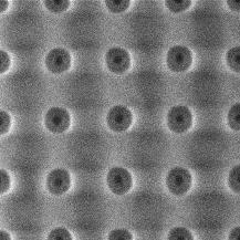
11 Single Contact Shrink Quantitative evaluation for multiple runs with random initial conditions opening yield: probability to obtain a single cylinder diameter of cylinder of minority block (CD) and template error enhancement factor (TEEF) Y. Ma, L. Lei, A. Torres et al., J. Micro/Nanolith. MEMS MOEMS., 2015, 14,
12 Outline Introduction Modeling approaches for DSA, Ohta-Kawasaki model, experimental process flow, coupled litho-dsa simulations Contact hole shrink Parameter calibration and comparison with experiment Contact multiplication Comparison with experimentally observed morphologies, multiple runs with random initial conditions, impact of segregation strength on process windows Conclusions 12
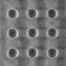
13 Contact Multiplication Basic phenomenon Resist profile / Guiding pattern after litho Block copolymer after DSA annealing previous modeling studies: A. Latypov et al.: Jpn. J. Appl. Phys. 53 (2014) 06JC01. M. Muramatsu et al.: Proc. SPIE 9049 (2014) N. Laachi et al.: Journal of Polymer Science Part B: Polymer Physics 53 (2015) here: focus on impact of guiding pattern neutral affinity of substrate mostly 2D 13
14 Contact Multiplication Comparison to experiment: calibrated model single contact shrink a = e 2 = 1.4 A. A. Gharbi, R. Tiron, M. Argoud et al., SPIE Advanced Lithography


15 Contact Multiplication Multiple runs with random initial conditions fluctuations of the number of cylinders: increase with aspect ratio very high in transition regions 15

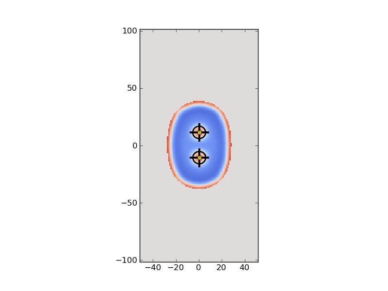

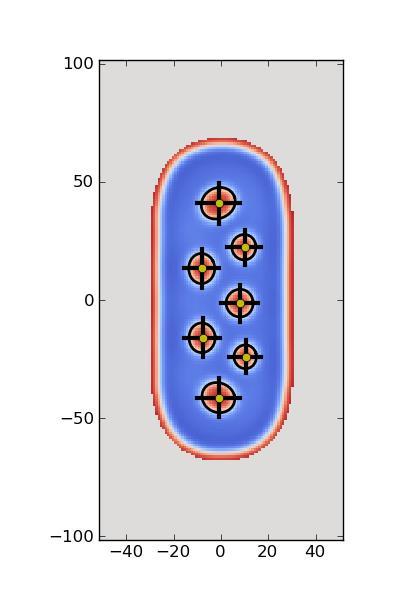

16 Contact Multiplication Metrology extraction of number, positions and sizes of cylinders 16
17 Contact Multiplication Quantitative evaluation for multiple runs with random initial conditions number of cylinders position (y) + CD (x/y), position (x) process windows width guiding pattern: 55nm scaling factor: s=1.0 17


18 Contact Multiplication Impact of scaling factor / segregation strength large process windows require: appropriate L 0 and cn width guiding pattern: 55nm 18


19 Contact Multiplication Impact of width of guiding pattern scaling factor: s=1.2 19
 low segregation (s=2.")
20 Contact Multiplication Prediction of 3D Ohta-Kawasaki model high segregation (s=1.0) low segregation (s=2.0) 20
 of the block copolymers OK model can predict morphologies and their sensitivities to variation of")

21 Conclusions DSA process windows are determined by the natural period L 0 and by the segregation strength (cn) of the block copolymers OK model can predict morphologies and their sensitivities to variation of the lithographically fabricated guiding pattern Quantitative predictability of OK-model depends on: natural period L 0 : a combination of a and e with segregation strength: scaling factor s surface affinities 21

22 Acknowledgements Thanks to the CoLiSA.MMP project consortium The research leading to these results has received funding from the European Union Seventh Framework Programme (FP7/ ) under grant agreement no CoLiSA.MMP. 22
 low segregation (s=2.")
23 Single Contact Shrink Prediction of 3D Ohta-Kawasaki model high segregation (s=1.0) low segregation (s=2.0) 23
TEMPLATE AFFINITY ROLE IN CONTACT SHRINK BY DSA PLANARIZATION
 TEMPLATE AFFINITY ROLE IN CONTACT SHRINK BY DSA PLANARIZATION A. Gharbi, R. Tiron, M. Argoud, P. Pimenta Barros, S. Bos, G. Chamiotmaitral, I. Servin, A. Fouquet, J. Hazart (CEA-LETI) X. Chevalier, C.
Technologies VII. Alternative Lithographic PROCEEDINGS OF SPIE. Douglas J. Resnick Christopher Bencher. Sponsored by. Cosponsored by.
 PROCEEDINGS OF SPIE Alternative Lithographic Technologies VII Douglas J. Resnick Christopher Bencher Editors 23-26 February 2015 San Jose, California, United States Sponsored by SPIE Cosponsored by DNS
SEMATECH Knowledge Series 2010
 SEMATECH Knowledge Series 2010 Summary of the SEMATECH Workshop on Directed Self Assembly Lloyd Litt SEMATECH/GF Bill Hinsberg - IBM 20 October 2010 Kobe, Japan Copyright 2010 Advanced Materials Research
Lithography Challenges Moore s Law Rising Costs and Challenges of Advanced Patterning
 Lithography Challenges Moore s Law Rising Costs and Challenges of Advanced Patterning SEMI Texas Spring Forum May 21, 2013 Austin, Texas Author / Company / Division / Rev. / Date A smartphone today has
Introduction to / Status of Directed Self- Assembly
 Introduction to / Status of Directed Self- Assembly DSA Workshop, Kobe Japan, October 2010 Bill Hinsberg IBM Almaden Research Center San Jose CA 95120 hnsbrg@almaden.ibm.com 2010 IBM Corporation from Bringing
Metrology for block copolymer directed self-assembly structures using Mueller matrix-based scatterometry
 Metrology for block copolymer directed self-assembly structures using Mueller matrix-based scatterometry Dhairya J. Dixit Vimal Kamineni Richard Farrell Erik R. Hosler Moshe Preil Joseph Race Brennan Peterson
Spectroscopic Critical Dimension technology (SCD) for Directed Self Assembly
 for Directed Self Assembly") Spectroscopic Critical Dimension technology (SCD) for Directed Self Assembly Senichi Nishibe a, Thaddeus Dziura a, Venkat Nagaswami a, Roel Gronheid b a KLA-Tencor Corporation, 1 Technology Drive, Milpitas
Spectroscopic Critical Dimension technology (SCD) for Directed Self Assembly Senichi Nishibe a, Thaddeus Dziura a, Venkat Nagaswami a, Roel Gronheid b a KLA-Tencor Corporation, 1 Technology Drive, Milpitas
Applicable Simulation Methods for Directed Self-Assembly -Advantages and Disadvantages of These Methods
 Review Applicable Simulation Methods for Directed Self-Assembly -Advantages and Disadvantages of These Methods Hiroshi Morita Journal of Photopolymer Science and Technology Volume 26, Number 6 (2013) 801
Techniken der Oberflächenphysik (Techniques of Surface Physics)
") Techniken der Oberflächenphysik (Techniques of Surface Physics) Prof. Yong Lei & Dr. Yang Xu (& Liying Liang) Fachgebiet 3D-Nanostrukturierung, Institut für Physik Contact: yong.lei@tu-ilmenau.de; yang.xu@tu-ilmenau.de;
Techniken der Oberflächenphysik (Techniques of Surface Physics) Prof. Yong Lei & Dr. Yang Xu (& Liying Liang) Fachgebiet 3D-Nanostrukturierung, Institut für Physik Contact: yong.lei@tu-ilmenau.de; yang.xu@tu-ilmenau.de;
Nanostructured Materials and New Processing Strategies Through Polymer Chemistry
 Nanostructured Materials and New Processing Strategies Through Polymer Chemistry Professor Christopher J. Ellison McKetta Department of Chemical Engineering and Texas Materials Institute The University
Variability-Aware Compact Model Strategy for 20-nm Bulk MOSFET
 Variability-Aware Compact Model Strategy for 20-nm Bulk MOSFET X. Wang 1, D. Reid 2, L. Wang 1, A. Burenkov 3, C. Millar 2, B. Cheng 2, A. Lange 4, J. Lorenz 3, E. Baer 3, A. Asenov 1,2! 1 Device Modelling
Optical characterization of highly inhomogeneous thin films
 Optical characterization of highly inhomogeneous thin films D.M. Rosu, A. Hertwig, P. Petrik, U. Beck Department 6.7 - Surface Modification and Measurement Technique BAM - Federal Institute for Materials
ALIGNMENT ACCURACY IN A MA/BA8 GEN3 USING SUBSTRATE CONFORMAL IMPRINT LITHOGRAPHY (SCIL)
") ALIGNMENT ACCURACY IN A MA/BA8 GEN3 USING SUBSTRATE CONFORMAL IMPRINT LITHOGRAPHY (SCIL) Robert Fader Fraunhofer Institute for Integrated Systems and Device Technology (IISB) Germany Ulrike Schömbs SUSS
ALIGNMENT ACCURACY IN A MA/BA8 GEN3 USING SUBSTRATE CONFORMAL IMPRINT LITHOGRAPHY (SCIL) Robert Fader Fraunhofer Institute for Integrated Systems and Device Technology (IISB) Germany Ulrike Schömbs SUSS
Supporting Online Material. Directed Assembly of Block Copolymer Blends into Non-regular Device Oriented Structures
 Supporting Online Material Directed Assembly of Block Copolymer Blends into Non-regular Device Oriented Structures Mark P. Stoykovich, 1 Marcus Müller, 2 Sang Ouk Kim, 1* Harun H. Solak, 3 Erik W. Edwards,
OVERVIEW OF THE SUPERTHEME PROJECT
 OVERVIEW OF THE SUPERTHEME PROJECT Conference Sponsors: OUTLINE 1. Introduction 2. Background pillars: Process and device 3. Consortium and project data 4. Project structure 5. Methodology used 6. Example:
OPTICAL DIAGNOSTICS TO STUDY SUPERCRITICAL CO 2 PROCESSES. A. Braeuer
 OPTICAL DIAGNOSTICS TO STUDY SUPERCRITICAL CO 2 PROCESSES A. Braeuer Lehrstuhl für Technische Thermodynamik (LTT) and Erlangen Graduate School in Advanced Optical Technologies (SAOT), Friedrich-Alexander
Study of Block Copolymer Lithography using SCFT: New Patterns and Methodology
 Study of Block Copolymer Lithography using SCFT: New Patterns and Methodology Su-Mi Hur Glenn Fredrickson Complex Fluids Design Consortium Annual Meeting Monday, February 2, 2009 Materials Research Laboratory
The SMART Process for Directed Block Co-Polymer Self-Assembly
 Journal of Photopolymer Science and Technology Volume 26, Number 5 (2013) 573 579 2013SPST The SMART Process for Directed Block Co-Polymer Self-Assembly Jihoon Kim*, Jingxiu Wan, Shinji Miyazaki, Jian
SUPPLEMENTARY INFORMATION
 SUPPLEMENTARY INFORMATION Towards wafer-size graphene layers by atmospheric pressure graphitization of silicon carbide Supporting online material Konstantin V. Emtsev 1, Aaron Bostwick 2, Karsten Horn
Directed Self-assembly of Topcoat-free Polycarbonate-containing High-χ Block Copolymers
 Directed Self-assembly of Topcoat-free Polycarbonate-containing High-χ Block Copolymers, Kristin Schmidt, Gabriela Alva, Noel Arellano, Teddie Magbitang, Anindarupa Chunder, Melia Tjio, Elizabeth Lofano,
Imaging Polymer Morphology Using Atomic Force Microscopy
 Imaging Polymer Morphology Using Atomic Force Microscopy Russell J. Composto Materials Science and Engineering, and the Laboratory for Research on the Structure of Matter, University of Pennsylvania Agilent
Electron-beam SAFIER process and its application for magnetic thin-film heads
 Electron-beam SAFIER process and its application for magnetic thin-film heads XiaoMin Yang, a) Harold Gentile, Andrew Eckert, and Stanko R. Brankovic Seagate Research Center, 1251 Waterfront Place, Pittsburgh,
We are IntechOpen, the world s leading publisher of Open Access books Built by scientists, for scientists. International authors and editors
 We are IntechOpen, the world s leading publisher of Open Access books Built by scientists, for scientists 3,500 108,000 1.7 M Open access books available International authors and editors Downloads Our
Supplementary Materials for
 advances.sciencemag.org/cgi/content/full/1/10/e1500751/dc1 Supplementary Materials for Uniform metal nanostructures with long-range order via three-step hierarchical self-assembly The PDF file includes:
ADVANCED STORAGE TECHNOLOGY CONSORTIUM RESEARCH PROPOSAL TEMPLATE
 ADVANCED STORAGE TECHNOLOGY CONSORTIUM RESEARCH PROPOSAL TEMPLATE RADIALLY ORDERED BIT PATTERNED MEDIA USING A COMBINATION OF NANOIMPRINT LITHOGRAPHY AND SELF-ASSEMBLY AND FABRICATION OF PATTERN MEDIA
EUREKA: A new Industry EUV Research Center at LBNL
 EUREKA: A new Industry EUV Research Center at LBNL Patrick Naulleau Center for X-ray Optics Lawrence Berkeley National Laboratory Berkeley Lab MSD Materials Sciences Division 1 Operating model Core operational
Pattern Collapse. T h e L i t h o g r a p h y E x p e r t (November 2006) Chris A. Mack, Austin, Texas
 Chris A. Mack, Austin, Texas") Tutor55.doc: Version 8/10/06 T h e L i t h o g r a p h y E x p e r t (November 2006) Pattern Collapse Chris A. Mack, Austin, Texas Not long ago, defining what an acceptable resist profile looked like was
Tutor55.doc: Version 8/10/06 T h e L i t h o g r a p h y E x p e r t (November 2006) Pattern Collapse Chris A. Mack, Austin, Texas Not long ago, defining what an acceptable resist profile looked like was
Field-based Simulations for Block Copolymer Lithography (Self-Assembly of Diblock Copolymer Thin Films in Square Confinement)
") Field-based Simulations for Block Copolymer Lithography (Self-Assembly of Diblock Copolymer Thin Films in Square Confinement) Su-Mi Hur Glenn H. Fredrickson Complex Fluids Design Consortium Annual Meeting
Field-based Simulations for Block Copolymer Lithography (Self-Assembly of Diblock Copolymer Thin Films in Square Confinement) Su-Mi Hur Glenn H. Fredrickson Complex Fluids Design Consortium Annual Meeting
Simulation and characterization of surface and line edge roughness in photoresists before and after etching
 Simulation and characterization of surface and line edge roughness in photoresists before and after etching Motivation of this work : Sub 100nm lithographic features often suffer from roughness. Need to
EUV Resist-Fundamental Research
 EUV Resist-Fundamental Research Akinori Saeki, Hiroki Yamamoto, Takahiro Kozawa, and Seiichi Tagawa The Institute of Scientific and Industrial Research, Osaka University CREST, Japan Science and Technology
Integrated measuring system for MEMS
 Integrated measuring system for MEMS Thermal characterization of gas flows under slip-flow regime Alice Vittoriosi May 16, 2011 I NSTITUTE FOR M ICRO P ROCESS E NGINEERING - T HERMAL P ROCESS E NGINEERING
Positioning, Structuring and Controlling with Nanoprecision
 Positioning, Structuring and Controlling with Nanoprecision Regine Hedderich 1,2, Tobias Heiler 2,3, Roland Gröger 2,3, Thomas Schimmel 2,3 and Stefan Walheim 2,3 1 Network NanoMat 2 Institute of Nanotechnology,
Kim, Sang Ouk
 Directed Block Copolymer Assembly Integrated with Conventional ArF or I-line lithography Kim, ang Ouk (sangouk.kim@kaist.ac.kr) oft Nanomaterials Laboratory (http://snml.kaist.ac.kr) Department of Materials
Low Power Phase Change Memory via Block Copolymer Self-assembly Technology
 Low Power Phase Change Memory via Block Copolymer Self-assembly Technology Beom Ho Mun 1, Woon Ik Park 1, You Yin 2, Byoung Kuk You 1, Jae Jin Yun 1, Kung Ho Kim 1, Yeon Sik Jung 1*, and Keon Jae Lee 1*
2 Current status of the project
 1 Background The current research project started in September 2015 and its objective was to prepare and characterizise supramolecular block copolymer thin lms. Special interest was to study whether it
Variable capacitor energy harvesting based on polymer dielectric and composite electrode
 2.8.215 Variable capacitor energy harvesting based on polymer dielectric and composite electrode Robert Hahn 1*, Yuja Yang 1, Uwe Maaß 1, Leopold Georgi 2, Jörg Bauer 1, and K.- D. Lang 2 1 Fraunhofer
Thermal experimental & simulation investigations on new lead frame based LED packages.
 Thermal experimental & simulation investigations on new lead frame based LED packages. B. Pardo, A. Piveteau, J. Routin, S, A. Gasse, T. van Weelden* CEA-Leti, MINATEC Campus, 17 rue des Martyrs, 38054
Photonic band gaps with layer-by-layer double-etched structures
 Photonic band gaps with layer-by-layer double-etched structures R. Biswas a) Microelectronics Research Center, Ames Laboratory USDOE and Department of Physics and Astronomy, Iowa State University, Ames,
Optical Proximity Correction
 Optical Proximity Correction Mask Wafer *Auxiliary features added on mask 1 Overlay Errors + + alignment mask wafer + + photomask plate Alignment marks from previous masking level 2 (1) Thermal run-in/run-out
Evolution of micro-structures on silicon substrates by surface. Osaka University
 Evolution of micro-structures on silicon substrates by surface diffusion Koichi Sudoh The Institute of Scientific ifi and Industrial Research Osaka University Microstructure Fabrication applying Spontaneous
Positioning, Structuring and Controlling with Nanoprecision
 Positioning, Structuring and Controlling with Nanoprecision Regine Hedderich 1,2, Tobias Heiler 2,3, Roland Gröger 2,3, Thomas Schimmel 2,3, and Stefan Walheim 2,3 1 Network NanoMat 2 Institute of Nanotechnology,
Assessing Temperature Dependence of Drift. Mobility in Methylammonium Lead Iodide
 Supporting Information Assessing Temperature Dependence of Drift Mobility in Methylammonium Lead Iodide Perovskite Single Crystals Shreetu Shrestha, Gebhard J. Matt*, Andres Osvet, Daniel Niesner, Rainer
Supporting Information. A differential Hall effect measurement method with. sub-nanometre resolution for active dopant
 Supporting Information for A differential Hall effect measurement method with sub-nanometre resolution for active dopant concentration profiling in ultrathin doped Si 1 x Ge x and Si layers Richard Daubriac*
Mueller Matrix Polarimetry: A Powerful Tool for Nanostructure Metrology
 ECS Transactions, 6 () 237-242 (24).49/6.237ecst The Electrochemical Society Mueller Matrix Polarimetry: A Powerful Tool for Nanostructure Metrology Shiyuan Liu *, Xiuguo Chen, and Chuanwei Zhang State
Swing Curves. T h e L i t h o g r a p h y T u t o r (Summer 1994) Chris A. Mack, FINLE Technologies, Austin, Texas
 Chris A. Mack, FINLE Technologies, Austin, Texas") T h e L i t h o g r a p h y T u t o r (Summer 1994) Swing Curves Chris A. Mack, FINLE Technologies, Austin, Texas In the last edition of this column, we saw that exposing a photoresist involves the propagation
T h e L i t h o g r a p h y T u t o r (Summer 1994) Swing Curves Chris A. Mack, FINLE Technologies, Austin, Texas In the last edition of this column, we saw that exposing a photoresist involves the propagation
Raman spectroscopy of self-assembled InAs quantum dots in wide-bandgap matrices of AlAs and aluminium oxide
 Mat. Res. Soc. Symp. Proc. Vol. 737 2003 Materials Research Society E13.8.1 Raman spectroscopy of self-assembled InAs quantum dots in wide-bandgap matrices of AlAs and aluminium oxide D. A. Tenne, A. G.
Three Approaches for Nanopatterning
 Three Approaches for Nanopatterning Lithography allows the design of arbitrary pattern geometry but maybe high cost and low throughput Self-Assembly offers high throughput and low cost but limited selections
Scaling up Chemical Vapor Deposition Graphene to 300 mm Si substrates
 Scaling up Chemical Vapor Deposition Graphene to 300 mm Si substrates Co- Authors Aixtron Alex Jouvray Simon Buttress Gavin Dodge Ken Teo The work shown here has received partial funding from the European
High-density data storage: principle
 High-density data storage: principle Current approach High density 1 bit = many domains Information storage driven by domain wall shifts 1 bit = 1 magnetic nanoobject Single-domain needed Single easy axis
Superconducting Ti/TiN thin films for mm wave absorption
 Superconducting /N thin films for mm wave absorption A.Aliane 1, M. Solana 2, V. Goudon 1, C. Vialle 1, S. Pocas 1, E. Baghe 1, L. Carle 1, W. Rabaud 1, L. Saminadayar 2, L. Dussopt 1, P.Agnese 1, N. Lio
Sensors and Metrology. Outline
 Sensors and Metrology A Survey 1 Outline General Issues & the SIA Roadmap Post-Process Sensing (SEM/AFM, placement) In-Process (or potential in-process) Sensors temperature (pyrometry, thermocouples, acoustic
ORION NanoFab: An Overview of Applications. White Paper
 ORION NanoFab: An Overview of Applications White Paper ORION NanoFab: An Overview of Applications Author: Dr. Bipin Singh Carl Zeiss NTS, LLC, USA Date: September 2012 Introduction With the advancement
Südliche Stadtmauerstr. 15a Tel: D Erlangen Fax:
 Curriculum Vitae Lionel Santinacci 19.10.1974 Nationality: French Südliche Stadtmauerstr. 15a Tel: + 49 9131 852 7587 D-91054 Erlangen Fax: + 49 9131 852 7582 Germany e-mail: lionel@ww.uni-erlangen.de
Study of Deprotection Reaction during Exposure in Chemically Amplified Resists for Lithography Simulation
 Study of Deprotection Reaction during Exposure in hemically Amplified Resists for Lithography Simulation Yasuhiro Miyake, Mariko Isono and Atsushi Sekiguchi Litho Tech Japan orporation, 2-6-6-201, Namiki,
Effect of PAG Location on Resists for Next Generation Lithographies
 Effect of PAG Location on Resists for Next Generation Lithographies ber Research Group Materials Science & Engineering Ithaca, NY 14853 Development Trends in Microlithography 10 Contact Printer Architectures
Stochastic modeling of photoresist development in two and three dimensions
 J. Micro/Nanolith. MEMS MOEMS 9(4), 04202 (Oct Dec 200) Stochastic modeling of photoresist development in two and three dimensions Chris A. Mack 605 Watchhill Road Austin, Texas 78703 E-mail: chris@lithoguru.com
Spectroscopic Ellipsometry (SE) in Photovoltaic Applications
 in Photovoltaic Applications") Spectroscopic Ellipsometry (SE) in Photovoltaic Applications Jianing Sun, James Hilfiker, Greg Pribil, and John Woollam c-si PVMC Metrology Workshop July 2012, San Francisco PV key issues Material selection
Spectroscopic Ellipsometry (SE) in Photovoltaic Applications Jianing Sun, James Hilfiker, Greg Pribil, and John Woollam c-si PVMC Metrology Workshop July 2012, San Francisco PV key issues Material selection
PHYSICAL SELF-ASSEMBLY AND NANO-PATTERNING*
 Mater. Res. Soc. Symp. Proc. Vol. 849 2005 Materials Research Society KK8.4.1 PHYSICAL SELF-ASSEMBLY AND NANO-PATTERNING* T.-M. Lu, D.-X. Ye, T. Karabacak, and G.-C. Wang, Department of Physics, Applied
Unconventional Nano-patterning. Peilin Chen
 Unconventional Nano-patterning Peilin Chen Reference Outlines History of patterning Traditional Nano-patterning Unconventional Nano-patterning Ancient Patterning "This is the Elks' land". A greeting at
Characterizing Closure-phase Measurements at IOTA
 Characterizing Closure-phase Measurements at IOTA Ragland, S. 1,2,3, Traub, W. 1, Berger, J.-P. 4, Millan-Gabet, R. 5, Monnier, J. D. 6, Pedretti, E. 6, Schloerb, F. P. 7, Carleton, N. P. 1, Haguenauer,
Fundamental aspects of Photosensitized chemically amplified resist (PSCAR) and CAR: How to overcome RLS trade-off and photon shot noise problems
 and CAR: How to overcome RLS trade-off and photon shot noise problems") Fundamental aspects of Photosensitized chemically amplified resist (PSCAR) and CAR: How to overcome RLS trade-off and photon shot noise problems Seiichi Tagawa The Institute of Scientific and Industrial
Fundamental aspects of Photosensitized chemically amplified resist (PSCAR) and CAR: How to overcome RLS trade-off and photon shot noise problems Seiichi Tagawa The Institute of Scientific and Industrial
Polarons in Narrow Band-Gap Polymers Probed over the Entire IR Range: a Joint. Experimental and Theoretical Investigation
 Supporting Information for Polarons in Narrow Band-Gap Polymers Probed over the Entire IR Range: a Joint Experimental and Theoretical Investigation Simon Kahmann, 1,2 Daniele Fazzi, 3 Gebhard J. Matt,
 Citation Bram Lips, Robert Puers, (2016), Three step deep reactive ion etch for high density trench etching Journal of Physics: Conference Series, 757, 012005. Archived version Author manuscript: the content
Chapter 2 Process Variability. Overview. 2.1 Sources and Types of Variations
 Chapter 2 Process Variability Overview Parameter variability has always been an issue in integrated circuits. However, comparing with the size of devices, it is relatively increasing with technology evolution,
Design Study. Carl Zeiss Microelectronic Systems GmbH Enabling the Nano-Age World
 Carl Zeiss Microelectronic Systems GmbH Enabling the Nano-Age World,AIMS EUV Development Design Study Karl-Heinz Bechstein, Mathias Esselbach, Wolfgang Harnisch, Norbert Rosenkranz, Thomas Scherübl, Holger
A Computationally Efficient Method for Three-Dimensional Simulation of Ion Implantation
 1259 PAPER Special Issue on SISPAD 99 A Computationally Efficient Method for Three-Dimensional Simulation of Ion Implantation Alexander BURENKOV a), Klaus TIETZEL, Andreas HÖSSINGER,Jürgen LORENZ, Heiner
Cost of Ownership Considerations for Maskless Lithography
 Accelerating the next technology revolution Cost of Ownership Considerations for Maskless Lithography Lloyd C. Litt, SEMATECH Andrea F. Wüest, SEMATECH Copyright 2008 SEMATECH, Inc. SEMATECH, and the SEMATECH
Tilted ion implantation as a cost-efficient sublithographic
 Tilted ion implantation as a cost-efficient sublithographic patterning technique Sang Wan Kim 1,a), Peng Zheng 1, Kimihiko Kato 1, Leonard Rubin 2, Tsu-Jae King Liu 1 1 Department of Electrical Engineering
Stable DRIE-patterned SiO 2 /Si 3 N 4 electrets for electret-based vibration energy harvesters
 Stable DRIE-patterned SiO 2 /Si 3 N 4 electrets for electret-based vibration energy harvesters S. Boisseau 1,2, A.B. Duret 1, G. Despesse 1, J.J. Chaillout 1, J.S. Danel 1, A. Sylvestre 2 1 CEA, Leti,
Vassilios Constantoudis 1.2, Vijayakumar M. Kuppuswamy 1, Evangelos Gogolides 1.2
 1 Vassilios Constantoudis 1.2, Vijayakumar M. Kuppuswamy 1, Evangelos Gogolides 1.2 1 Institute of Nanoscience and Nanotechnology, NCSR Demokritos, Greece 2 Nanometrisis Co. Hari Pathangi Sriraman, Roel
Surface and line-edge roughness in solution and plasma developed negative tone resists: Experiment and simulation
 Surface and line-edge roughness in solution and plasma developed negative tone resists: Experiment and simulation G. P. Patsis, A. Tserepi, I. Raptis, N. Glezos, and E. Gogolides a) Institute of Microelectronics,
Functional Materials for Advanced Patterning Robert D. Allen. IBM Almaden Research Center
 Functional Materials for Advanced Patterning Robert D. Allen Business Unit or Product Name IBM Almaden Research Center 2003 IBM Corporation Resists/Materials for Advanced Patterning Trends in Lithography
Development of Lift-off Photoresists with Unique Bottom Profile
 Transactions of The Japan Institute of Electronics Packaging Vol. 8, No. 1, 2015 [Technical Paper] Development of Lift-off Photoresists with Unique Bottom Profile Hirokazu Ito, Kouichi Hasegawa, Tomohiro
Resist material for negative tone development process
 Resist material for negative tone development process FUJIFILM Corporation Electronic Materials Research Laboratories P-1 Outline 1. Advantages of negative tone imaging for DP 2. Process maturity of negative
Enhanced High Aspect Ratio Etch Performance With ANAB Technology. Keywords: High Aspect Ratio, Etch, Neutral Particles, Neutral Beam I.
 Enhanced High Aspect Ratio Etch Performance With ANAB Technology. Keywords: High Aspect Ratio, Etch, Neutral Particles, Neutral Beam I. INTRODUCTION As device density increases according to Moore s law,
Photonics applications 5: photoresists
 IMI-NFG s Mini Course on Chalcogenide Glasses Lecture 11 Photonics applications 5: photoresists Himanshu Jain Department of Materials Science & Engineering Lehigh University, Bethlehem, PA 18015 H.Jain@Lehigh.edu
Alignment of Liquid Crystals by Ion Etched Grooved Glass Surfaces. Yea-Feng Lin, Ming-Chao Tsou, and Ru-Pin Pan
 CHINESE JOURNAL OF PHYSICS VOL. 43, NO. 6 DECEMBER 2005 Alignment of Liquid Crystals by Ion Etched Grooved Glass Surfaces Yea-Feng Lin, Ming-Chao Tsou, and Ru-Pin Pan Department of Electrophysics, National
Ebeam based mask repair as door opener for defect free EUV masks M. Waiblinger a, Tristan Bret a, R. Jonckheere b, D.
 Ebeam based mask repair as door opener for defect free EUV masks M. Waiblinger a, Tristan Bret a, R. Jonckheere b, D. Van den Heuvel b a Carl Zeiss SMS GmbH - Carl-Zeiss-Promenade 10, 07745 Jena, / Industriestraße
Recent progress in nanoparticle photoresist development for EUV lithography
 Recent progress in nanoparticle photoresist development for EUV lithography Kazuki Kasahara ab, Vasiliki Kosma b, Jeremy Odent b, Hong Xu b, Mufei Yu b, Emmanuel P. Giannelis b, Christopher K. Ober b a
Beatrice Beyer ISFOE 2014 Thessaloniki, Greece
 Beatrice Beyer ISFOE 2014 Thessaloniki, Greece What? Graphene which is both highly conductive and transparent Large volume production Process safety Proof of concept for use as transparent electrode Why?
IC Fabrication Technology
 IC Fabrication Technology * History: 1958-59: J. Kilby, Texas Instruments and R. Noyce, Fairchild * Key Idea: batch fabrication of electronic circuits n entire circuit, say 10 7 transistors and 5 levels
Line-Edge Roughness and the Impact of Stochastic Processes on Lithography Scaling for Moore s Law
 Line-Edge Roughness and the Impact of Stochastic Processes on Lithography Scaling for Moore s Law Chris A. Mack Lithoguru.com, 1605 Watchhill Rd, Austin, TX 78703 Abstract Moore s Law, the idea that every
Top down and bottom up fabrication
 Lecture 24 Top down and bottom up fabrication Lithography ( lithos stone / graphein to write) City of words lithograph h (Vito Acconci, 1999) 1930 s lithography press Photolithography d 2( NA) NA=numerical
Arborescent Polymers as Templates for the Preparation of Metallic Nanoparticles
 Arborescent Polymers as Templates for the Preparation of Metallic Nanoparticles Jason Dockendorff Department of Chemistry University of Waterloo Outline 1. 1. Focus and Purpose of of Research 2. 2. The
Optical Measurements of Critical Dimensions at Several Stages of the Mask Fabrication Process
 Optical Measurements of Critical Dimensions at Several Stages of the Mask Fabrication Process John C. Lam, Alexander Gray n&k Technology, Inc., Santa Clara, CA ABSTRACT Critical dimension (CD) metrology
Supplementary Figure 1 SEM images and corresponding Fourier Transformation of nanoparticle arrays before pattern transfer (left), after pattern
, after pattern") Supplementary Figure 1 SEM images and corresponding Fourier Transformation of nanoparticle arrays before pattern transfer (left), after pattern transfer but before pattern shrinkage (middle), and after
Supplementary Figure 1 SEM images and corresponding Fourier Transformation of nanoparticle arrays before pattern transfer (left), after pattern transfer but before pattern shrinkage (middle), and after
Deposition of volatile chlorohydric acid on Copper wafer depending on humidity and HCl airborne concentration
 2018 SPCC Surface Preparation and Cleaning Conference Minh-Phuong TRAN, CEA-Leti, minh-phuong.tran@cea.fr Hervé FONTAINE, CEA-Leti, herve.fontaine@cea.fr Paola GONZÁLEZ-AGUIRRE, Entegris, paola.gonzalez@entegris.com
Selective Processes: Challenges and Opportunities in Semiconductor Scaling
 Selective Processes: Challenges and Opportunities in Semiconductor Scaling June 4, 2018 Kandabara Tapily TEL Technology Center, America, LLC IITC 2018 Selective Deposition Workshop K. Tapily/ IITC 2018
Nucleon form factors and moments of parton distributions in twisted mass lattice QCD
 Nucleon form factors and moments of parton distributions in twisted mass lattice QCD C. Alexandrou (a,b), (a), C. Kallidonis (a), T. Korzec (a,c) (a) Department of Physics, University of Cyprus, P.O. Box
PROCEEDINGS OF SPIE. Scaling rules for the design of a narrow-band grating filter at the focus of a free-space beam
 PROCEEDINGS OF SPIE SPIEDigitalLibrary.org/conference-proceedings-of-spie Scaling rules for the design of a narrow-band grating filter at the focus of a free-space beam Eanuel Bonnet, Alain Cachard, Alexandre
SUPPLEMENTARY NOTES Supplementary Note 1: Fabrication of Scanning Thermal Microscopy Probes
 SUPPLEMENTARY NOTES Supplementary Note 1: Fabrication of Scanning Thermal Microscopy Probes Fabrication of the scanning thermal microscopy (SThM) probes is summarized in Supplementary Fig. 1 and proceeds
Process-Simulation-Flow And Metrology of VLSI Layout Fine- Features
 IOSR Journal of VLSI and Signal Processing (IOSR-JVSP) Volume 7, Issue 6, Ver. I (Nov.-Dec. 2017), PP 23-28 e-issn: 2319 4200, p-issn No. : 2319 4197 www.iosrjournals.org Process-Simulation-Flow And Metrology
IInstitute for. Using Power Line Modems Measurements for Degradation Detection on Power Lines
 Using Power Line Modems Measurements for Degradation Detection on Power Lines Florian Gruber, Andreas M. Lehmann, Johannes B. Huber, Ralf Müller Friedrich-Alexander-Universität Erlangen-Nürnberg Institute
Methodology of modeling and simulating line-end shortening effects in deep-uv resist
 Methodology of modeling and simulating line-end shortening effects in deep-uv resist Mosong Cheng*, Ebo Croffie, Andrew Neureuther Electronics Research Laboratory Department of Electrical Engineering and
Structuring and bonding of glass-wafers. Dr. Anke Sanz-Velasco
 Structuring and bonding of glass-wafers Dr. Anke Sanz-Velasco Outline IMT Why glass? Components for life science Good bond requirements and evaluation Wafer bonding 1. Fusion bonding 2. UV-adhesive bonding
Supplementary Figure S1. AFM images of GraNRs grown with standard growth process. Each of these pictures show GraNRs prepared independently,
 Supplementary Figure S1. AFM images of GraNRs grown with standard growth process. Each of these pictures show GraNRs prepared independently, suggesting that the results is reproducible. Supplementary Figure
Relationships between Stochastic Phenomena and Optical Contrast in Chemically Amplified Resist Process of Extreme Ultraviolet Lithography
 Journal of Photopolymer Science and Technology Volume 7, Number () 9 SPST Relationships between Stochastic Phenomena and Optical Contrast in Chemically Amplified Resist Process of Extreme Ultraviolet Lithography
Selective Manipulation of Molecules by Electrostatic Force and Detection of Single Molecules in Aqueous Solution
 Supporting Information Selective Manipulation of Molecules by Electrostatic Force and Detection of Single Molecules in Aqueous Solution Zhongbo Yan, Ming Xia, Pei Zhang, and Ya-Hong Xie* Department of
Deformable MEMS grating for wide tunability and high operating speed
 Deformable MEMS grating for wide tunability and high operating speed Maurizio Tormen (1), Yves-Alain Peter (2), Philippe Niedermann (1), Arno Hoogerwerf (1), Herbert Shea (3) and Ross Stanley (1) 1 Centre
Split-gate charge trap memories: impact of scaling on performances and consumption for low-power embedded applications
 Split-gate charge trap memories: impact of scaling on performances and consumption for low-power embedded applications Lia Masoero lia.masoero@cea.fr Outline Introduction Technological details Basics of