Characteristics of Neutral Beam Generated by a Low Angle Reflection and Its Etch Characteristics by Halogen-Based Gases
|
|
|
- Leslie Adams
- 6 years ago
- Views:
Transcription

1 Characteristics of Neutral Beam Generated by a Low Angle Reflection and Its Etch Characteristics by Halogen-Based Gases Geun-Young Yeom SungKyunKwan University
2 Problems of Current Etch Technology Scaling down of the device to nano-scale : increased volunability to processing damage - Physical damage - Electrical damage (Charging damage) DRAM Half Pitch Gate Length 2/32 SKKU

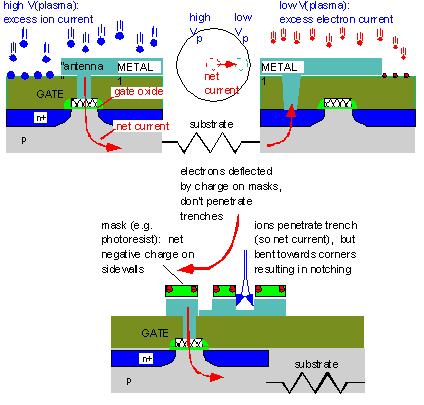
3 Charging Effects 3/32 SKKU

4 Trend of Etching Tools Development 4/32 SKKU
5 Researtch Status of Neutral Beam Etching Technologies 1) Gas dynamics or hyperthermal atomic beam (Heating of gas) - Caltech by Giapis in 2 (laser), PSI Inc. in 2 (laser), NEC by Nishiyama in 1995 (thermal heating), etc. Oklahoma Univ. in 2 (hyperthermal) 2) Ion-neutral scattering (charge exchange process) - Hitach by Mizutani in 1995 (ion removal by retarding grid), NTT by Matuso in 1995 (ion removal by magnetic field), etc. 3) Ion-electron recombination (surface neutralization) - IBM by Chen in 1997 (sheath recombination by ion and electron) - Tohoku University in 22 - Ebara Research Co. in 1995 (capillary hole) - Tokyo Univ. in 2 (focused fast atom beam) 5/32 SKKU

 6/32")
6 Neutral Beam Etching using Gas Dynamics PSI Inc. in 2 (laser) 6/32 SKKU
7 Researtch Status of Neutral Beam Etching Technologies 1) Gas dynamics or hyperthermal atomic beam (Heating of gas) - Caltech by Giapis in 2 (laser), PSI Inc. in 2 (laser), - NEC by Nishiyama in 1995 (thermal heating), etc. - Oklahoma Univ. in 2 (hyperthermal) 2) Ion-neutral scattering (charge exchange process) - Hitach by Mizutani in 1995 (ion removal by retarding grid), - NTT by Matuso in 1995 (ion removal by magnetic field), etc. 3) Ion-electron recombination (surface neutralization) - IBM by Chen in 1997 (sheath recombination by ion and electron) - Tohoku University in 22 - Ebara Research Co. in 1995 (capillary hole) - Tokyo Univ. in 2 (focused fast atom beam) 7/32 SKKU
8 Neutral Beam Etching by Ion - Neutral Scattering (Tatsumi Mizutani et. al, hitachi, 1995) 8/32 SKKU
9 Researtch Status of Neutral Beam Etching Technologies 1) Gas dynamics or hyperthermal atomic beam (Heating of gas) - Caltech by Giapis in 2 (laser), PSI Inc. in 2 (laser), NEC by Nishiyama in 1995 (thermal heating), etc. Oklahoma Univ. in 2 (hyperthermal) 2) Ion-neutral scattering (charge exchange process) - Hitach by Mizutani in 1995 (ion removal by retarding grid), NTT by Matuso in 1995 (ion removal by magnetic field), etc. 3) Ion-electron recombination (surface neutralization) - IBM by Chen in 1997 (sheath recombination by ion and electron) - Tohoku University in 22 - Ebara Research Co. in 1995 (capillary hole) - Tokyo Univ. in 2 (focused fast atom beam) 9/32 SKKU


10 Neutral beam etching by Ion-Electron Recombination (I) (Demetre J. Economou et.al, Houston Univ., 2) 1/32 SKKU

11 Generation of Directional Neutral Beam by Low Angle Reflection Recombination by low angle forward scattering 1~3 retarding grid reflection plate 9 5~15 Neutral beam Ion beam 5~15 Reflection plate : Si Ion gun O 2, SF 6 neutral beam ion beam faraday cup or sample rf coil When the ion beam was reflected by a reflector at the angles lower than 15, most of the ions reflected were neutralized and the lower reflector angle showed the higher degree of neutralization. 11/32 SKKU


12 Experimental Low Angle Reflected Neutral Beam System Quartz Plasma Electromagnet RF Coil Φ4 Acceleration Grid Focusing Grid 6 inch 25 mm Deceleration Grid Ion Beam Flux Plate-type type Reflector 5 o Reflection Angle Neutral Beam Flux Substrate 12/32 SKKU
13 Ion Flux and Neutral Flux as a function of Acceleration Voltage Ion current density (ua/cm 2 ) SF 6 SF 6 5 o reflection NF 3 NF 3 5 o reflection CF 4 CF 4 5 o reflection Ar Ar 5 o reflection Grid hole size:ø2 neutral beam retarding grid reflection plate ion beam rf faraday cup or sample coil Acceleration voltage (volts) 13/32 SKKU
14 SiO 2 Etch Rate as Functions of Acceleration Voltage and Gas Flow Rates for SF 6, NF 3, CF 4, and Ar Condition : reflector angle: 5, rf power: 5W SF 6 gas flow rate: 7 sccm Condition : reflector angle: 5, rf power: 5W Va : 7V SiO 2 etch rate ( nm/min. ) SF 6 NF 3 CF 4 Ar SiO 2 etch rate (nm/min.) SF 6 NF 3 CF 4 Ar Acceleration voltage (Volts) Flow rate (sccm) 14/32 SKKU
15 SiO 2 and Si Etch Rate as a Function of SF 6 Gas Flow Rate Condition : reflector angle: 5, rf power: 4W, distance between reflector and sample : 4 cm, pure SF 6, Va: 4 V, Ve: -1 V SiO Si Etch rate (A/min) Va: 4 V Ve: -1 V Flow rate (seem) Etch rate (A/min) Va: 4 V Ve: -1 V Flow rate (sccm) 15/32 SKKU
16 Etch Rate and Etch Selectivity as a Function of Gas Flow Rate Using the Neutral Beam Etching System Condition : rf power: 3W, acceleration voltage: 4V, reflector angle: 5 o reflector material: Si 5 4 Si SiO 2 PR Si/PR SiO 2 /PR Etch rate(a/min) Selectivity CF 4 flow rate (sccm) CF 4 flow rate (sccm) 16/32 SKKU
17 Etch Rate and Etch Selectivity as a Function of H 2 to CF 4 Using Neutral Beam Etching System Condition : rf power: 3W, CF 4 +H 2 : 15sccm, acceleration voltage: 4V, reflector material: metal, reflector angle: 5 o Etch rate(a/min) Si SiO 2 PR Etch selectivity Si/PR SiO 2 /PR H 2 /(H 2 +CF 4 )% H 2 /(H 2 +CF 4 )% 17/32 SKKU
 Condition : SF 6 2.")

18 SEM Micrograph of SiO 2 Etch Profiles (Neutral Beam Etching) Condition : SF sccm, rf power: 4 W, acceleration voltage: 4V, reflector angle: 5 o etch mask : Cr 18/32 SKKU


19 SEM Micrograph of Si Etch Profiles Condition : CF 4 15sccm, rf power: 3W, acceleration voltage: 4V, reflector material: metal, reflector angle: 5 o 19/32 SKKU
20 Effect of Reflector Angle on Reflected Angle and Flux of the Neutrals Condition : SF 6 1 sccm(.6 mtorr), rf power: 4W, acceleration voltage: 4V reflector material: Si SiO 2 etch depth(a) o 1 o 15 o 2 o SiO 2 etch depth(a) Reflected polar angle θ r ( o ) o 1 o 15 o 2 o Reflected polar angle θ r ( o ) 9 Incident ion energy: 4V SiO 2 etch depth(a) Incident ion energy: 4V 1 o 5 o SiO 2 etch depth(a) o 5 o Reflected azimuthal angle φ r ( o ) 4 5 Incident beam direction Reflected azimuthal angle φ r ( o ) 2/32 SKKU
21 Effect of Reflector Materials on Reflected Angle and Flux Condition : SF 6 1 sccm(.6 mtorr), rf power: 4W, acceleration voltage: 4V reflector angle: 5 o SiO 2 etch depth(a) Incident angle θ i : 5 o DLC Si Metal SiO SF Reflected polar angle θ r ( o ) 4 2 SiO 2 DLC Si Metal Reflected polar angle θ r ( o ) 21/32 SKKU
22 C-V V Characteristics Before and After Neutral Beam & ICP Etch Capacitance (F) 1.2E-1 1.E-1 8.E-11 6.E-11 4.E-11 reference neutral 3 min ICP 2 min Capacitance (F) 5.E-11 4.E-11 3.E-11 2.E-11 reference neutral 3 min ICP 2 min 2.E-11 1.E-11.E Voltage (V) Voltage (V) <Big dot: 3um x 3 um > <middle dot: 2um x2um> Al(5A) Si 3 N 4 (5nm) SiO 2 (2nm) Si p-type, (1)1Ωcm 22/32 SKKU
23 I-V V Characteristics Before and After Neutral Beam & ICP Etch Treatment -ICP plasma power: 5 W, bias voltage: -1 V, gas: O 2, time: 2 min - Neutral beam power: 5 W, acceleration voltage: 4V, extraction voltage: -1V gas: O 2, time: 3 min, distance: 5 cm Current (A) 5.x1-7 4.x1-7 3.x1-7 2.x1-7 1.x1-7. reference neutral beam etching ICP etching Voltage (V) <small dot: 1um x 1um> 5.x1-7 4.x1-7 reference neutral beam etching ICP etching 5.x1-7 4.x1-7 reference neutral beam etching ICP etching Current (A) 3.x1-7 2.x1-7 Current (A) 3.x1-7 2.x1-7 1.x1-7 1.x Voltage (V) <middle dot: 2um x2um> Voltage (V) <Big dot: 3um x 3 um > 23/32 SKKU
 condition : rf")
 (Poly-Si/SiO 2 ) 24/32")
24 SEM Micrograph of Poly-Si and Poly-Si/SiO 2 Etch Profiles (ICP Etching) condition : rf power: 7W, Bias voltage: -75V pure SF 6 5 mtorr, (Poly-Si) (Poly-Si/SiO 2 ) 24/32 SKKU
 condition : SF 6 2.")
, rf power: 4W, Ve: -1V, Va: 4V, etch")
25 SEM Micrograph of Poly-Si and Poly-Si/SiO 2 Etch Profiles (Ion Beam Etching) condition : SF sccm(.3 mtorr), rf power: 4W, Ve: -1V, Va: 4V, etch mask: Cr (Poly-Si) (Poly-Si/SiO 2 ) 25/32 SKKU

 condition :")


26 SEM Micrograph of poly-si and SiO 2 Etch Profiles (Neutral Beam Etching) condition : reflector angle: 5, SF sccm(.3 mtorr), rf power: 4W, Ve: -1V, Va: 4V (Poly-Si) (Poly-Si/SiO 2 ) 26/32 SKKU
27 GaN and GaAs Etching as a Function of Flow rate, Additive Gas Process conditions Fixed power : 4W, Fixed acceleration voltage : 4V Etch rate (Angstrom) GaAs GaN Etch rate (Angstrom) GaAs GaN Cl 2 flow rate (sccm) <Cl 2 Flow rate> Ar flow rate (sccm) <Cl 2 +Ar Flow rate> Total flow rate : 15sccm 27/32 SKKU
28 Damage Analysis Etched n-gan, GaAs Process conditions Fixed acceleration voltage : 4V, pure Cl 2, Gas flow rate : 3sccm, GaN Photoluminescence GaAs PhotoReflectrance Room Temp. PL Intensity (a.u.) As-received ICP treatment Neutral treatment R/R (arb. units) Reference ICP ethcing Neutral etching Wavelength (nm) <GaN PL> Photon energy (ev) <GaAs PRS> 28/32 SKKU
29 I-V V Characteristics of GaN LEDs after Neutral Beam Etching of p-gan Condition - Neutral beam etching : Power 4W / Bias +4V / CF 4 15sccm / 4min / thickness 6-65Å - ICP etching : Power 4W / Bias -4V / CF 4 15sccm / 15sec / thickness 75-8Å 1 8 Reference ICP etching Neutral beam etching Reference ICP etching Neutral beam etching.1 Current (ma) 6 4 LogA (ma).1 1E-3 1E-4 1E-5 2 1E-6 1E-7 1E-8 Device Structure Voltage (V) Voltage (V) p - contact : Cr/Au p - contact : ITO p - GaN P-GaN surface Hole size : 2μm Reference Multi quantum well n - contact : Ti/Al n - GaN Neutral beam etch ICP etch 29/32 SKKU
> Hole patterns <Neutral beam")
 1 8 6 4 2 42 44 46 48 5 52 Wave length (nm) Reference")

30 GaN Device Efficiency after Neutral Beam Etching of p-gan 12 <Reference (No pattern)> Hole patterns <Neutral beam etch (patterned)> Emission intensity (A.U) Wave length (nm) Reference Neutral beam textured Emission at 2mA Emission intensities were increased about 22% in neutral beam textured GaN LED (OES analysis) 3/32 SKKU

31 Commercialization Alpha Version for 12inch Dia.. Silicon Nano Processing RF Matcher Plasma source Grid & Reflector Chuck Process Chamber Pump Control box Item Ion source Grid & Reflector Chuck Chamber & Vacuum system Gas 사양 - Source type : ICP - Power 3W - Density : 5.5E+11(4mTorr, 25W) Grid Reflector Wafer - Grid에 DC Bias 인가 - Grid hole size; 2, 3, 4mm -Gridgap;2,4,6mm - Reflector angle; 3, 5, 7 + Plasma Chuck&reflectorgap;5,1,15mm - Grid material : Graphite + bias Control voltage Ground - Tilting(Manual, 45 ) & Rotating(Automatic, 15RPM) - Lift pin & Mechanical clamp - No Cooling & heating - Vertical type - Chamber pressure :.3mTorr with Ar 4sccm - TMP 42l/s - Gate valve : ø4, Step motor Operation(Pressure control) - Gas box type : IGS(1.25) - Gas line : 14 line < 설비구성 > < 설비사양 > 31/32 SKKU
32 Summary Using a low energy reflection of reactive ion beam, directional reactive neutral beam for chargeless etching was successfully fabricated. By using the neutral beam, nanoscale etching of silicon and silicon oxide could be achieved. No charging damage was detected by the use of the neutral beam while the conventional ICP etching showed a significant damage such as leakage of gate oxide, RIE-lag, etc. It is believed that, neutral beam etching technique is benificial for the nanodevice processing not only for the top-down devices but also for the bottom-up devices 32/32 SKKU
ETCHING Chapter 10. Mask. Photoresist
 ETCHING Chapter 10 Mask Light Deposited Substrate Photoresist Etch mask deposition Photoresist application Exposure Development Etching Resist removal Etching of thin films and sometimes the silicon substrate
Nanopantography: A method for parallel writing of etched and deposited nanopatterns
 Nanopantography: A method for parallel writing of etched and deposited nanopatterns Vincent M. Donnelly 1, Lin Xu 1, Azeem Nasrullah 2, Zhiying Chen 1, Sri C. Vemula 2, Manish Jain 1, Demetre J. Economou
H. Shin, W. Zhu, V. M. Donnelly, and D. J. Economou University of Houston. November 2, AVS 58h International Symposium, Nashville, TN, USA
 Near-Threshold Ion-Enhanced Silicon Etching H. Shin, W. Zhu, V. M. Donnelly, and D. J. Economou o ou University of Houston Acknowledgements: DOE Plasma Science Center, NSF and Varian Semiconductor Equipment
Etching Capabilities at Harvard CNS. March 2008
 Etching Capabilities at Harvard CNS March 2008 CNS: A shared use facility for the Harvard Community and New England CNS Provides technical support, equipment and staff. Explicitly multi-disciplinary w/
Etching Applications and Discoveries Made Possible by Advanced Ion Energy Control
 Etching Applications and Discoveries Made Possible by Advanced Ion Energy Control Possible by Advanced Ion Energy Control V. M. Donnelly Department of Chemical and Biomolecular Engineering University of
Plasma Chemistry Study in an Inductively Coupled Dielectric Etcher
 Plasma Chemistry Study in an Inductively Coupled Dielectric Etcher Chunshi Cui, John Trow, Ken Collins, Betty Tang, Luke Zhang, Steve Shannon, and Yan Ye Applied Materials, Inc. October 26, 2000 10/28/2008
E SC 412 Nanotechnology: Materials, Infrastructure, and Safety Wook Jun Nam
 E SC 412 Nanotechnology: Materials, Infrastructure, and Safety Wook Jun Nam Lecture 10 Outline 1. Wet Etching/Vapor Phase Etching 2. Dry Etching DC/RF Plasma Plasma Reactors Materials/Gases Etching Parameters
Chapter 7. Plasma Basics
 Chapter 7 Plasma Basics 2006/4/12 1 Objectives List at least three IC processes using plasma Name three important collisions in plasma Describe mean free path Explain how plasma enhance etch and CVD processes
The Stanford Nanofabrication Facility. Etch Area Overview. May 21, 2013
 The Stanford Nanofabrication Facility Etch Area Overview May 21, 2013 High Density Plasma Systems Etcher Materials Etched Gases available Wafer Size Applied Materials P5000 MRIE ChA Applied Materials P5000
Etching: Basic Terminology
 Lecture 7 Etching Etching: Basic Terminology Introduction : Etching of thin films and sometimes the silicon substrate are very common process steps. Usually selectivity, and directionality are the first
Chapter 7 Plasma Basic
 Chapter 7 Plasma Basic Hong Xiao, Ph. D. hxiao89@hotmail.com www2.austin.cc.tx.us/hongxiao/book.htm Hong Xiao, Ph. D. www2.austin.cc.tx.us/hongxiao/book.htm 1 Objectives List at least three IC processes
Wet and Dry Etching. Theory
 Wet and Dry Etching Theory 1. Introduction Etching techniques are commonly used in the fabrication processes of semiconductor devices to remove selected layers for the purposes of pattern transfer, wafer
Feature Profile Evolution during Shallow Trench Isolation (STI) Etch in Chlorine-based Plasmas
 Etch in Chlorine-based Plasmas") 1 Feature Profile Evolution during Shallow Trench Isolation (STI) Etch in Chlorine-based Plasmas Presentation November 14, 2005 Jane P. Chang and John Hoang Department of Chemical and Biomolecular Engineering
1 Feature Profile Evolution during Shallow Trench Isolation (STI) Etch in Chlorine-based Plasmas Presentation November 14, 2005 Jane P. Chang and John Hoang Department of Chemical and Biomolecular Engineering
MEGAWATT SOLID-STATE ELECTRONICS
 MATERIALS, PROCESS AND DEVICE DEVELOPMENT FOR GaN (and SiC) POWER DEVICES University of Florida: SRI: MCNC: Device Design/Simulation (In Collaboration with Sandia) Process Development Device Fabrication
CHAPTER 6: Etching. Chapter 6 1
 Chapter 6 1 CHAPTER 6: Etching Different etching processes are selected depending upon the particular material to be removed. As shown in Figure 6.1, wet chemical processes result in isotropic etching
DOE WEB SEMINAR,
 DOE WEB SEMINAR, 2013.03.29 Electron energy distribution function of the plasma in the presence of both capacitive field and inductive field : from electron heating to plasma processing control 1 mm PR
INVESTIGATION of Si and SiO 2 ETCH MECHANISMS USING an INTEGRATED SURFACE KINETICS MODEL
 46 th AVS International Symposium Oct. 25-29, 1999 Seattle, WA INVESTIGATION of Si and SiO 2 ETCH MECHANISMS USING an INTEGRATED SURFACE KINETICS MODEL Da Zhang* and Mark J. Kushner** *Department of Materials
INTRODUCTION TO THE HYBRID PLASMA EQUIPMENT MODEL
 INTRODUCTION TO THE HYBRID PLASMA EQUIPMENT MODEL Prof. Mark J. Kushner Department of Electrical and Computer Engineering 1406 W. Green St. Urbana, IL 61801 217-144-5137 mjk@uiuc.edu http://uigelz.ece.uiuc.edu
Plasma Technology September 15, 2005 A UC Discovery Project
 1 Feature-level Compensation & Control Plasma Technology September 15, 2005 A UC Discovery Project 9/15/05 - Plasma Technology 2 Plasma Technology Professors Jane P. Chang (UCLA), Michael A. Lieberman,
Chapter 2 On-wafer UV Sensor and Prediction of UV Irradiation Damage
 Chapter 2 On-wafer UV Sensor and Prediction of UV Irradiation Damage Abstract UV radiation during plasma processing affects the surface of materials. Nevertheless, the interaction of UV photons with surface
Enhanced High Aspect Ratio Etch Performance With ANAB Technology. Keywords: High Aspect Ratio, Etch, Neutral Particles, Neutral Beam I.
 Enhanced High Aspect Ratio Etch Performance With ANAB Technology. Keywords: High Aspect Ratio, Etch, Neutral Particles, Neutral Beam I. INTRODUCTION As device density increases according to Moore s law,
Plasma-Surface Interactions in Patterning High-k k Dielectric Materials
 Plasma-Surface Interactions in Patterning High-k k Dielectric Materials October 11, 4 Feature Level Compensation and Control Seminar Jane P. Chang Department of Chemical Engineering University of California,
LECTURE 5 SUMMARY OF KEY IDEAS
 LECTURE 5 SUMMARY OF KEY IDEAS Etching is a processing step following lithography: it transfers a circuit image from the photoresist to materials form which devices are made or to hard masking or sacrificial
MODELING OF SEASONING OF REACTORS: EFFECTS OF ION ENERGY DISTRIBUTIONS TO CHAMBER WALLS*
 MODELING OF SEASONING OF REACTORS: EFFECTS OF ION ENERGY DISTRIBUTIONS TO CHAMBER WALLS* Ankur Agarwal a) and Mark J. Kushner b) a) Department of Chemical and Biomolecular Engineering University of Illinois,
Section 3: Etching. Jaeger Chapter 2 Reader
 Section 3: Etching Jaeger Chapter 2 Reader Etch rate Etch Process - Figures of Merit Etch rate uniformity Selectivity Anisotropy d m Bias and anisotropy etching mask h f substrate d f d m substrate d f
DEPOSITION OF THIN TiO 2 FILMS BY DC MAGNETRON SPUTTERING METHOD
 Chapter 4 DEPOSITION OF THIN TiO 2 FILMS BY DC MAGNETRON SPUTTERING METHOD 4.1 INTRODUCTION Sputter deposition process is another old technique being used in modern semiconductor industries. Sputtering
Plasma etching. Bibliography
 Plasma etching Bibliography 1. B. Chapman, Glow discharge processes, (Wiley, New York, 1980). - Classical plasma processing of etching and sputtering 2. D. M. Manos and D. L. Flamm, Plasma etching; An
Chapter 2 FABRICATION PROCEDURE AND TESTING SETUP. Our group has been working on the III-V epitaxy light emitting materials which could be
 Chapter 2 7 FABRICATION PROCEDURE AND TESTING SETUP 2.1 Introduction In this chapter, the fabrication procedures and the testing setups for the sub-micrometer lasers, the submicron disk laser and the photonic
Reactive Ion Etching (RIE)
") Reactive Ion Etching (RIE) RF 13.56 ~ MHz plasma Parallel-Plate Reactor wafers Sputtering Plasma generates (1) Ions (2) Activated neutrals Enhance chemical reaction 1 2 Remote Plasma Reactors Plasma Sources
Reactive Ion Etching (RIE) RF 13.56 ~ MHz plasma Parallel-Plate Reactor wafers Sputtering Plasma generates (1) Ions (2) Activated neutrals Enhance chemical reaction 1 2 Remote Plasma Reactors Plasma Sources
Supplementary Figure 1 Detailed illustration on the fabrication process of templatestripped
 Supplementary Figure 1 Detailed illustration on the fabrication process of templatestripped gold substrate. (a) Spin coating of hydrogen silsesquioxane (HSQ) resist onto the silicon substrate with a thickness
Hong Young Chang Department of Physics, Korea Advanced Institute of Science and Technology (KAIST), Republic of Korea
, Republic of Korea") Hong Young Chang Department of Physics, Korea Advanced Institute of Science and Technology (KAIST), Republic of Korea Index 1. Introduction 2. Some plasma sources 3. Related issues 4. Summary -2 Why is
Hong Young Chang Department of Physics, Korea Advanced Institute of Science and Technology (KAIST), Republic of Korea Index 1. Introduction 2. Some plasma sources 3. Related issues 4. Summary -2 Why is
Lecture 15 Etching. Chapters 15 & 16 Wolf and Tauber. ECE611 / CHE611 Electronic Materials Processing Fall John Labram 1/76
 Lecture 15 Etching Chapters 15 & 16 Wolf and Tauber 1/76 Announcements Term Paper: You are expected to produce a 4-5 page term paper on a selected topic (from a list). Term paper contributes 25% of course
Plasma Processing in the Microelectronics Industry. Bert Ellingboe Plasma Research Laboratory
 Plasma Processing in the Microelectronics Industry Bert Ellingboe Plasma Research Laboratory Outline What has changed in the last 12 years? What is the relavant plasma physics? Sheath formation Sheath
PARTICLE CONTROL AT 100 nm NODE STATUS WORKSHOP: PARTICLES IN PLASMAS
 PARTICLE CONTROL AT 100 nm NODE STATUS WORKSHOP: PARTICLES IN PLASMAS Mark J. Kushner University of Illinois Department of Electrical and Computer Engineering Urbana, IL 61801 mjk@uiuc.edu December 1998
4FNJDPOEVDUPS 'BCSJDBUJPO &UDI
 2010.5.4 1 Major Fabrication Steps in CMOS Process Flow UV light oxygen Silicon dioxide Silicon substrate Oxidation (Field oxide) photoresist Photoresist Coating Mask exposed photoresist Mask-Wafer Exposed
Etching Issues - Anisotropy. Dry Etching. Dry Etching Overview. Etching Issues - Selectivity
 Etching Issues - Anisotropy Dry Etching Dr. Bruce K. Gale Fundamentals of Micromachining BIOEN 6421 EL EN 5221 and 6221 ME EN 5960 and 6960 Isotropic etchants etch at the same rate in every direction mask
UNIT 3. By: Ajay Kumar Gautam Asst. Prof. Dev Bhoomi Institute of Technology & Engineering, Dehradun
 UNIT 3 By: Ajay Kumar Gautam Asst. Prof. Dev Bhoomi Institute of Technology & Engineering, Dehradun 1 Syllabus Lithography: photolithography and pattern transfer, Optical and non optical lithography, electron,
Dielectric Meta-Reflectarray for Broadband Linear Polarization Conversion and Optical Vortex Generation
 Supporting Information Dielectric Meta-Reflectarray for Broadband Linear Polarization Conversion and Optical Vortex Generation Yuanmu Yang, Wenyi Wang, Parikshit Moitra, Ivan I. Kravchenko, Dayrl P. Briggs,
Classification of Solids
 Classification of Solids Classification by conductivity, which is related to the band structure: (Filled bands are shown dark; D(E) = Density of states) Class Electron Density Density of States D(E) Examples
Supplementary Information Our InGaN/GaN multiple quantum wells (MQWs) based one-dimensional (1D) grating structures
 based one-dimensional (1D) grating structures") Polarized white light from hybrid organic/iii-nitrides grating structures M. Athanasiou, R. M. Smith, S. Ghataora and T. Wang* Department of Electronic and Electrical Engineering, University of Sheffield,
Polarized white light from hybrid organic/iii-nitrides grating structures M. Athanasiou, R. M. Smith, S. Ghataora and T. Wang* Department of Electronic and Electrical Engineering, University of Sheffield,
Nova 600 NanoLab Dual beam Focused Ion Beam IITKanpur
 Nova 600 NanoLab Dual beam Focused Ion Beam system @ IITKanpur Dual Beam Nova 600 Nano Lab From FEI company (Dual Beam = SEM + FIB) SEM: The Electron Beam for SEM Field Emission Electron Gun Energy : 500
SCALING OF HOLLOW CATHODE MAGNETRONS FOR METAL DEPOSITION a)
") SCALING OF HOLLOW CATHODE MAGNETRONS FOR METAL DEPOSITION a) Gabriel Font b) Novellus Systems, Inc. San Jose, CA, 95134 USA and Mark J. Kushner Dept. of Electrical and Computer Engineering Urbana, IL,
SCALING OF HOLLOW CATHODE MAGNETRONS FOR METAL DEPOSITION a) Gabriel Font b) Novellus Systems, Inc. San Jose, CA, 95134 USA and Mark J. Kushner Dept. of Electrical and Computer Engineering Urbana, IL,
Lecture 6 Plasmas. Chapters 10 &16 Wolf and Tauber. ECE611 / CHE611 Electronic Materials Processing Fall John Labram 1/68
 Lecture 6 Plasmas Chapters 10 &16 Wolf and Tauber 1/68 Announcements Homework: Homework will be returned to you on Thursday (12 th October). Solutions will be also posted online on Thursday (12 th October)
Chapter 8 Ion Implantation
 Chapter 8 Ion Implantation 2006/5/23 1 Wafer Process Flow Materials IC Fab Metalization CMP Dielectric deposition Test Wafers Masks Thermal Processes Implant PR strip Etch PR strip Packaging Photolithography
Ion Implantation. alternative to diffusion for the introduction of dopants essentially a physical process, rather than chemical advantages:
 Ion Implantation alternative to diffusion for the introduction of dopants essentially a physical process, rather than chemical advantages: mass separation allows wide varies of dopants dose control: diffusion
Room temperature synthesis of GaN driven by kinetic. energy be-yond the limit of thermodynamics
 Supporting Information Room temperature synthesis of GaN driven by kinetic energy be-yond the limit of thermodynamics Takane Imaoka 1,4,5, Takeru Okada 2,4, Seiji Samukawa 2,3,4*, and Kimihisa Yamamoto
Direct Measurement of Adhesion Energy of Monolayer Graphene As-Grown. on Copper and Its Application to Renewable Transfer Process
 SUPPORTING INFORMATION Direct Measurement of Adhesion Energy of Monolayer Graphene As-Grown on Copper and Its Application to Renewable Transfer Process Taeshik Yoon 1, Woo Cheol Shin 2, Taek Yong Kim 2,
Carbon Nanotube Thin-Films & Nanoparticle Assembly
 Nanodevices using Nanomaterials : Carbon Nanotube Thin-Films & Nanoparticle Assembly Seung-Beck Lee Division of Electronics and Computer Engineering & Department of Nanotechnology, Hanyang University,
Multicolor Graphene Nanoribbon/Semiconductor Nanowire. Heterojunction Light-Emitting Diodes
 Multicolor Graphene Nanoribbon/Semiconductor Nanowire Heterojunction Light-Emitting Diodes Yu Ye, a Lin Gan, b Lun Dai, *a Hu Meng, a Feng Wei, a Yu Dai, a Zujin Shi, b Bin Yu, a Xuefeng Guo, b and Guogang
EE 527 MICROFABRICATION. Lecture 25 Tai-Chang Chen University of Washington
 EE 527 MICROFABRICATION Lecture 25 Tai-Chang Chen University of Washington ION MILLING SYSTEM Kaufmann source Use e-beam to strike plasma A magnetic field applied to increase ion density Drawback Low etch
Plasma Deposition (Overview) Lecture 1
 Lecture 1") Plasma Deposition (Overview) Lecture 1 Material Processes Plasma Processing Plasma-assisted Deposition Implantation Surface Modification Development of Plasma-based processing Microelectronics needs (fabrication
Plasma Deposition (Overview) Lecture 1 Material Processes Plasma Processing Plasma-assisted Deposition Implantation Surface Modification Development of Plasma-based processing Microelectronics needs (fabrication
Edgeless sensors for full-field X-ray imaging
 Edgeless sensors for full-field X-ray imaging 12 th iworid in Cambridge July 14 th, 2010 Marten Bosma 12 th iworid, Cambridge - July 14 th, 2010 Human X-ray imaging High spatial resolution Low-contrast
Industrial Applications of Ultrafast Lasers: From Photomask Repair to Device Physics
 Industrial Applications of Ultrafast Lasers: From Photomask Repair to Device Physics Richard Haight IBM TJ Watson Research Center PO Box 218 Yorktown Hts., NY 10598 Collaborators Al Wagner Pete Longo Daeyoung
UNIVERSITY OF CALIFORNIA College of Engineering Department of Electrical Engineering and Computer Sciences. Fall Exam 1
 UNIVERSITY OF CALIFORNIA College of Engineering Department of Electrical Engineering and Computer Sciences EECS 143 Fall 2008 Exam 1 Professor Ali Javey Answer Key Name: SID: 1337 Closed book. One sheet
Effect of Noble Gas. Plasma Processing Laboratory University of Houston. Acknowledgements: DoE Plasma Science Center and NSF
 Ion Energy Distributions in Pulsed Plasmas with Synchronous DC Bias: Effect of Noble Gas W. Zhu, H. Shin, V. M. Donnelly and D. J. Economou Plasma Processing Laboratory University of Houston Acknowledgements:
Plasma etch control by means of physical plasma parameter measurement with HERCULES Sematech AEC/APC Symposium X
 Plasma etch control by means of physical plasma parameter measurement with HERCULES A. Steinbach F. Bell D. Knobloch S. Wurm Ch. Koelbl D. Köhler -1- Contents - Introduction - Motivation - Plasma monitoring
3.155J/6.152J Microelectronic Processing Technology Fall Term, 2004
 3.155J/6.152J Microelectronic Processing Technology Fall Term, 2004 Bob O'Handley Martin Schmidt Quiz Nov. 17, 2004 Ion implantation, diffusion [15] 1. a) Two identical p-type Si wafers (N a = 10 17 cm
Effect of Gas Flow Rate and Gas Composition in Ar/CH 4 Inductively Coupled Plasmas
 COMSOL CONFERENCE BOSTON 2011 Effect of Gas Flow Rate and Gas Composition in Ar/CH 4 Inductively Coupled Plasmas Keisoku Engineering System Co., Ltd., JAPAN Dr. Lizhu Tong October 14, 2011 1 Contents 1.
NNCI ETCH WORKSHOP - STANFORD NNCI PLASMA ETCH OVERVIEW. Usha Raghuram Stanford Nanofabrication Facility Stanford, CA May 24, 2016
 NNCI ETCH WORKSHOP - STANFORD NNCI PLASMA ETCH OVERVIEW Usha Raghuram Stanford Nanofabrication Facility Stanford, CA May 24, 2016 NNCI AT STANFORD Four labs under NNCI Umbrella at Stanford SNSF Stanford
Quantum Technology: Supplying the Picks and Shovels
 Quantum Technology: Supplying the Picks and Shovels Dr John Burgoyne Quantum Control Engineering: Mathematical Solutions for Industry Open for Business Event 7 th August 2014, 12.30-17.00, Isaac Newton
MICROCHIP MANUFACTURING by S. Wolf
 by S. Wolf Chapter 15 ALUMINUM THIN-FILMS and SPUTTER-DEPOSITION 2004 by LATTICE PRESS CHAPTER 15 - CONTENTS Aluminum Thin-Films Sputter-Deposition Process Steps Physics of Sputter-Deposition Magnetron-Sputtering
Gaetano L Episcopo. Scanning Electron Microscopy Focus Ion Beam and. Pulsed Plasma Deposition
 Gaetano L Episcopo Scanning Electron Microscopy Focus Ion Beam and Pulsed Plasma Deposition Hystorical background Scientific discoveries 1897: J. Thomson discovers the electron. 1924: L. de Broglie propose
Traps in MOCVD n-gan Studied by Deep Level Transient Spectroscopy and Minority Carrier Transient Spectroscopy
 Traps in MOCVD n-gan Studied by Deep Level Transient Spectroscopy and Minority Carrier Transient Spectroscopy Yutaka Tokuda Department of Electrical and Electronics Engineering, Aichi Institute of Technology,
Physique des plasmas radiofréquence Pascal Chabert
 Physique des plasmas radiofréquence Pascal Chabert LPP, Ecole Polytechnique pascal.chabert@lpp.polytechnique.fr Planning trois cours : Lundi 30 Janvier: Rappels de physique des plasmas froids Lundi 6 Février:
EFFECT OF REACTOR GEOMETRY ON ION ENERGY DISTRIBUTIONS FOR PULSED PLASMA DOPING (P 2 LAD)*
*") EFFECT OF REACTOR GEOMETRY ON ION ENERGY DISTRIBUTIONS FOR PULSED PLASMA DOPING (P 2 LAD)* Ankur Agarwal a) and Mark J. Kushner b) a) Department of Chemical and Biomolecular Engineering University of Illinois
EFFECT OF REACTOR GEOMETRY ON ION ENERGY DISTRIBUTIONS FOR PULSED PLASMA DOPING (P 2 LAD)* Ankur Agarwal a) and Mark J. Kushner b) a) Department of Chemical and Biomolecular Engineering University of Illinois
Defect management and control. Tsuyoshi Moriya, PhD Senior Manager Tokyo Electron Limited
 Defect management and control Tsuyoshi Moriya, PhD Senior Manager Tokyo Electron Limited Background Case study: A maintainer has good hands Only he achieved good yield for every maintenance But... He could
Anisotropic etching of polymer films by high energy È100s of ev oxygen atom neutral beams
 Anisotropic etching of polymer films by high energy È100s of ev oxygen atom neutral beams Siddhartha Panda and Demetre J. Economou a) Plasma Processing Laboratory, Department of Chemical Engineering, University
MODELING OF AN ECR SOURCE FOR MATERIALS PROCESSING USING A TWO DIMENSIONAL HYBRID PLASMA EQUIPMENT MODEL. Ron L. Kinder and Mark J.
 TECHCON 98 Las Vegas, Nevada September 9-11, 1998 MODELING OF AN ECR SOURCE FOR MATERIALS PROCESSING USING A TWO DIMENSIONAL HYBRID PLASMA EQUIPMENT MODEL Ron L. Kinder and Mark J. Kushner Department of
Dry Etching Zheng Yang ERF 3017, MW 5:15-6:00 pm
 Dry Etching Zheng Yang ERF 3017, email: yangzhen@uic.edu, MW 5:15-6:00 pm Page 1 Page 2 Dry Etching Why dry etching? - WE is limited to pattern sizes above 3mm - WE is isotropic causing underetching -
Three Approaches for Nanopatterning
 Three Approaches for Nanopatterning Lithography allows the design of arbitrary pattern geometry but maybe high cost and low throughput Self-Assembly offers high throughput and low cost but limited selections
Regents of the University of California
 Deep Reactive-Ion Etching (DRIE) DRIE Issues: Etch Rate Variance The Bosch process: Inductively-coupled plasma Etch Rate: 1.5-4 μm/min Two main cycles in the etch: Etch cycle (5-15 s): SF 6 (SF x+ ) etches
Advances in Back-side Via Etching of SiC for GaN Device Applications
 Advances in Back-side Via Etching of SiC for GaN Device Applications Anthony Barker, Kevin Riddell, Huma Ashraf & Dave Thomas SPTS Technologies, Ringland Way, Newport NP18 2TA, UK, dave.thomas@spts.com,
CVD: General considerations.
 CVD: General considerations. PVD: Move material from bulk to thin film form. Limited primarily to metals or simple materials. Limited by thermal stability/vapor pressure considerations. Typically requires
Lecture 10. Vacuum Technology and Plasmas Reading: Chapter 10. ECE Dr. Alan Doolittle
 Lecture 10 Vacuum Technology and Plasmas Reading: Chapter 10 Vacuum Science and Plasmas In order to understand deposition techniques such as evaporation, sputtering,, plasma processing, chemical vapor
UHF-ECR Plasma Etching System for Dielectric Films of Next-generation Semiconductor Devices
 UHF-ECR Plasma Etching System for Dielectric Films of Next-generation Semiconductor Devices 1 UHF-ECR Plasma Etching System for Dielectric Films of Next-generation Semiconductor Devices Katsuya Watanabe
ELEC 7364 Lecture Notes Summer Etching. by STELLA W. PANG. from The University of Michigan, Ann Arbor, MI, USA
 ELEC 7364 Lecture Notes Summer 2008 Etching by STELLA W. PANG from The University of Michigan, Ann Arbor, MI, USA Visiting Professor at The University of Hong Kong The University of Michigan on Visiting
X-Ray Photoelectron Spectroscopy (XPS) Prof. Paul K. Chu
 Prof. Paul K. Chu") X-Ray Photoelectron Spectroscopy (XPS) Prof. Paul K. Chu X-ray Photoelectron Spectroscopy Introduction Qualitative analysis Quantitative analysis Charging compensation Small area analysis and XPS imaging
X-Ray Photoelectron Spectroscopy (XPS) Prof. Paul K. Chu X-ray Photoelectron Spectroscopy Introduction Qualitative analysis Quantitative analysis Charging compensation Small area analysis and XPS imaging
EFFECT OF PRESSURE AND ELECTRODE SEPARATION ON PLASMA UNIFORMITY IN DUAL FREQUENCY CAPACITIVELY COUPLED PLASMA TOOLS *
 EFFECT OF PRESSURE AND ELECTRODE SEPARATION ON PLASMA UNIFORMITY IN DUAL FREQUENCY CAPACITIVELY COUPLED PLASMA TOOLS * Yang Yang a) and Mark J. Kushner b) a) Department of Electrical and Computer Engineering
EE C245 ME C218 Introduction to MEMS Design Fall 2007
 EE C245 ME C218 Introduction to MEMS Design Fall 2007 Prof. Clark T.-C. Nguyen Dept. of Electrical Engineering & Computer Sciences University of California at Berkeley Berkeley, CA 94720 Lecture 12: Mechanics
A Photonic Crystal Laser from Solution Based. Organo-Lead Iodide Perovskite Thin Films
 SUPPORTING INFORMATION A Photonic Crystal Laser from Solution Based Organo-Lead Iodide Perovskite Thin Films Songtao Chen 1, Kwangdong Roh 2, Joonhee Lee 1, Wee Kiang Chong 3,4, Yao Lu 5, Nripan Mathews
Characterization of an Oxygen Plasma by Using a Langmuir Probe in an Inductively Coupled Plasma
 Journal of the Korean Physical Society, Vol. 38, No. 3, March 001, pp. 59 63 Characterization of an Oxygen Plasma by Using a Langmuir Probe in an Inductively Coupled Plasma Jong-Sik Kim and Gon-Ho Kim
EE 527 MICROFABRICATION. Lecture 24 Tai-Chang Chen University of Washington
 EE 527 MICROFABRICATION Lecture 24 Tai-Chang Chen University of Washington EDP ETCHING OF SILICON - 1 Ethylene Diamine Pyrocatechol Anisotropy: (100):(111) ~ 35:1 EDP is very corrosive, very carcinogenic,
Self-Assembled InAs Quantum Dots
 Self-Assembled InAs Quantum Dots Steve Lyon Department of Electrical Engineering What are semiconductors What are semiconductor quantum dots How do we make (grow) InAs dots What are some of the properties
Two-dimensional Bragg grating lasers defined by electron-beam lithography
 Two-dimensional Bragg grating lasers defined by electron-beam lithography Guy A. DeRose a Pasadena, California 91125 and Department of Applied Physics, California Institute of Technology, 1200 E. California
Normally-Off GaN Field Effect Power Transistors: Device Design and Process Technology Development
 Center for High Performance Power Electronics Normally-Off GaN Field Effect Power Transistors: Device Design and Process Technology Development Dr. Wu Lu (614-292-3462, lu.173@osu.edu) Dr. Siddharth Rajan
Introduction to X-ray Photoelectron Spectroscopy (XPS) XPS which makes use of the photoelectric effect, was developed in the mid-1960
 XPS which makes use of the photoelectric effect, was developed in the mid-1960") Introduction to X-ray Photoelectron Spectroscopy (XPS) X-ray Photoelectron Spectroscopy (XPS), also known as Electron Spectroscopy for Chemical Analysis (ESCA) is a widely used technique to investigate
Introduction to X-ray Photoelectron Spectroscopy (XPS) X-ray Photoelectron Spectroscopy (XPS), also known as Electron Spectroscopy for Chemical Analysis (ESCA) is a widely used technique to investigate
CURRENT STATUS OF NANOIMPRINT LITHOGRAPHY DEVELOPMENT IN CNMM
 U.S. -KOREA Forums on Nanotechnology 1 CURRENT STATUS OF NANOIMPRINT LITHOGRAPHY DEVELOPMENT IN CNMM February 17 th 2005 Eung-Sug Lee,Jun-Ho Jeong Korea Institute of Machinery & Materials U.S. -KOREA Forums
Inductively Coupled Plasma Etching of Ta, Co, Fe, NiFe, NiFeCo, and MnNi with Cl 2 /Ar Discharges
 Korean J. Chem. Eng., 21(6), 1235-1239 (2004) Inductively Coupled Plasma Etching of Ta, Co, Fe, NiFe, NiFeCo, and MnNi with Cl 2 /Ar Discharges Hyung Jo Park*, Hyun-Wook Ra, Kwang Sup Song** and Yoon-Bong
Nanoimprint Lithography
 Nanoimprint Lithography Wei Wu Quantum Science Research Advanced Studies HP Labs, Hewlett-Packard Email: wei.wu@hp.com Outline Background Nanoimprint lithography Thermal based UV-based Applications based
~1 V ~20-40 V. Electron collector PLASMA. Ion extraction optics. Ionization zone. Mass Resolving section Ion detector. e - ~20 V Filament Heater
 RGAs and Leak detectors [Note that standard Ion Implanters are just overgrown RGAs!] RGAs or Residual Gas Analyzers are also known as Mass Spectrum Analyzers. These can sometimes be upgraded to also include
1 P a g e h t t p s : / / w w w. c i e n o t e s. c o m / Physics (A-level)
") 1 P a g e h t t p s : / / w w w. c i e n o t e s. c o m / Physics (A-level) Electromagnetic induction (Chapter 23): For a straight wire, the induced current or e.m.f. depends on: The magnitude of the magnetic
1 P a g e h t t p s : / / w w w. c i e n o t e s. c o m / Physics (A-level) Electromagnetic induction (Chapter 23): For a straight wire, the induced current or e.m.f. depends on: The magnitude of the magnetic
Lithography and Etching
 Lithography and Etching Victor Ovchinnikov Chapters 8.1, 8.4, 9, 11 Previous lecture Microdevices Main processes: Thin film deposition Patterning (lithography) Doping Materials: Single crystal (monocrystal)
DO NOT WRITE YOUR NAME OR KAUST ID NUMBER ON THIS PAGE OR ANY OTHER PAGE PUT YOUR EXAM ID NUMBER ON THIS PAGE AND EVERY OTHER PAGE YOU SUBMIT
 DO NOT WRITE YOUR NAME OR KAUST ID NUMBER ON THIS PAGE OR ANY OTHER PAGE PUT YOUR EXAM ID NUMBER ON THIS PAGE AND EVERY OTHER PAGE YOU SUBMIT WRITE YOUR SOLUTIONS ON ONLY ONE SIDE OF EMPTY SOLUTION SHEETS
Plasma based modification of thin films and nanoparticles. Johannes Berndt, GREMI,Orléans
 Plasma based modification of thin films and nanoparticles Johannes Berndt, GREMI,Orléans What is a plasma? A plasma is a ionized quasineutral gas! + electron electrons Neon bottle Ne atom Ne ion: Ne +
Tool- and pattern-dependent spatial variations in silicon deep reactive ion etching
 Tool- and pattern-dependent spatial variations in silicon deep reactive ion etching Hayden Taylor Microsystems Technology Laboratories Massachusetts Institute of Technology 12 May 2006 Coping with spatial
Large Scale Direct Synthesis of Graphene on Sapphire and Transfer-free Device Fabrication
 Supplementary Information Large Scale Direct Synthesis of Graphene on Sapphire and Transfer-free Device Fabrication Hyun Jae Song a, Minhyeok Son a, Chibeom Park a, Hyunseob Lim a, Mark P. Levendorf b,
Figure 1: Graphene release, transfer and stacking processes. The graphene stacking began with CVD
 Supplementary figure 1 Graphene Growth and Transfer Graphene PMMA FeCl 3 DI water Copper foil CVD growth Back side etch PMMA coating Copper etch in 0.25M FeCl 3 DI water rinse 1 st transfer DI water 1:10
Combinatorial RF Magnetron Sputtering for Rapid Materials Discovery: Methodology and Applications
 Combinatorial RF Magnetron Sputtering for Rapid Materials Discovery: Methodology and Applications Philip D. Rack,, Jason D. Fowlkes,, and Yuepeng Deng Department of Materials Science and Engineering University
EE-612: Lecture 22: CMOS Process Steps
 EE-612: Lecture 22: CMOS Process Steps Mark Lundstrom Electrical and Computer Engineering Purdue University West Lafayette, IN USA Fall 2006 NCN www.nanohub.org Lundstrom EE-612 F06 1 outline 1) Unit Process
Modification of thin films and nanoparticles. Johannes Berndt, GREMI,Orléans
 Modification of thin films and nanoparticles Johannes Berndt, GREMI,Orléans Low temperature plasmas not fully ionized Ionization degree 10-6 10-4 far away from thermodynamic equlilibrium T electron >>