Quantum Technology: Supplying the Picks and Shovels
|
|
|
- Oswald Johns
- 5 years ago
- Views:
Transcription
1 Quantum Technology: Supplying the Picks and Shovels Dr John Burgoyne Quantum Control Engineering: Mathematical Solutions for Industry Open for Business Event 7 th August 2014, , Isaac Newton Institute, Cambridge Page 1


2 Why picks and shovels? 20 February 2006 Tools enable discovery Page 2
3 Behind the metaphor New ideas + New tools = New science Page 3

, Mgt Science,")

4 Von Hippel (1978), J. Marketing, Jan 1978, 36 Von Hippel (1986), Mgt Science, 32 7, 791 Why this dialogue is important Page 4


5 A suite of materials, metrology and measurement tools for QT MBE & UHV sputtering fabrication Surface analysis - chemical SEM Qbit measurement Surface analysis - structural Plasma deposition and etch Qbit manipulation Page 5

6 Device fabrication Page 6


")


7 Enabling device fabrication via a suite of advanced techniques and processes Growth MBE Nanowires/nanotubes High temperature plasmaenhanced chemical vapour deposition (PECVD) Deposition PECVD Inductively coupled plasma (ICP) deposition Ion beam deposition Atomic layer deposition (ALD) Etch ICP etch Reactive ion etch (RIE) Ion beam etch Page 7


8 Capabilities from research to pilot-scale and production solutions that grow with the technology 50 mm Wafer size 450 mm Open load Wafer handling Production cassette to cassette Page 8
 PECVD Sputter ICP-CVD #1")

9 Multi-tool clusters ALD (thermal & plasma) PECVD Sputter ICP-CVD #1 Hex handler with integrated Kelvin Probe Kelvin probe ICP-CVD #2 Page 9


 HB LED substrate etch SiC metal mask")
10 Our process advantage Process library of > 6,000 processes developed over 25 years Accessible to all our customers Close collaboration with major Universities and R&D facilities Caltech, Cornell, LBNL, TU Eindhoven, IMEC, Southampton University, Cambridge University, Process guarantees for key parameters Including wafer-to-wafer repeatability for rate and uniformity TEOS based SiO 2 deposition Waveguide etch Typical GaN etched feature (PR remains intact) HB LED substrate etch SiC metal mask etch High rate SiN x at 8 0ºC Page 10


11 Extreme aspect ratio conformal deposition via Atomic Layer Deposition Unique capability of ALD for monatomic/ mono-molecular layer control over extremely high aspect ratio features Example (top): ALD of Al 2 O 3 on carbon nanotubes (CNT) Using TMA and O 2 plasma O2 plasma just enough to react with TMA but not etch CNT No additional functionalisation of CNT necessary Example (bottom): 20 nm HfO 2 onto 25:1 AR Si trenches Conformality ~ 100% Trench corner Trench bottom HfO 2 Si HfO 2 Si Page 11


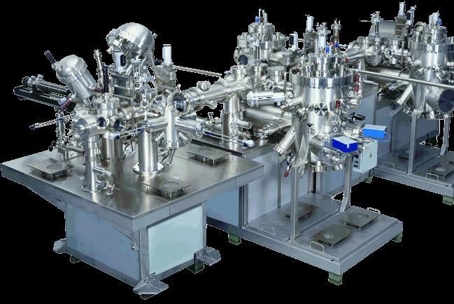
12 Deposition UHV multi-chamber tool: Institute for Quantum Computing, University of Waterloo, Canada Page 12
13 Deposition UHV multi-chamber tool: Institute for Quantum Computing, University of Waterloo, Canada MBE and UHV sputtering methods on multiple materials within the same device Metals, metal oxides, superconductors, topological insulators XPS (X-ray photoelectron spectroscopy) analysis of samples Oxford Instruments Omicron ARGUS analyser In-process analysis Enables layer-by-layer quality control of the MBE and sputtering growth processes Page 13

14 Device physics and characterisation Page 14
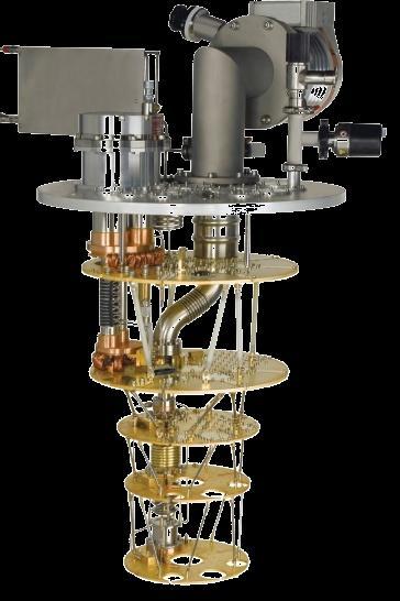
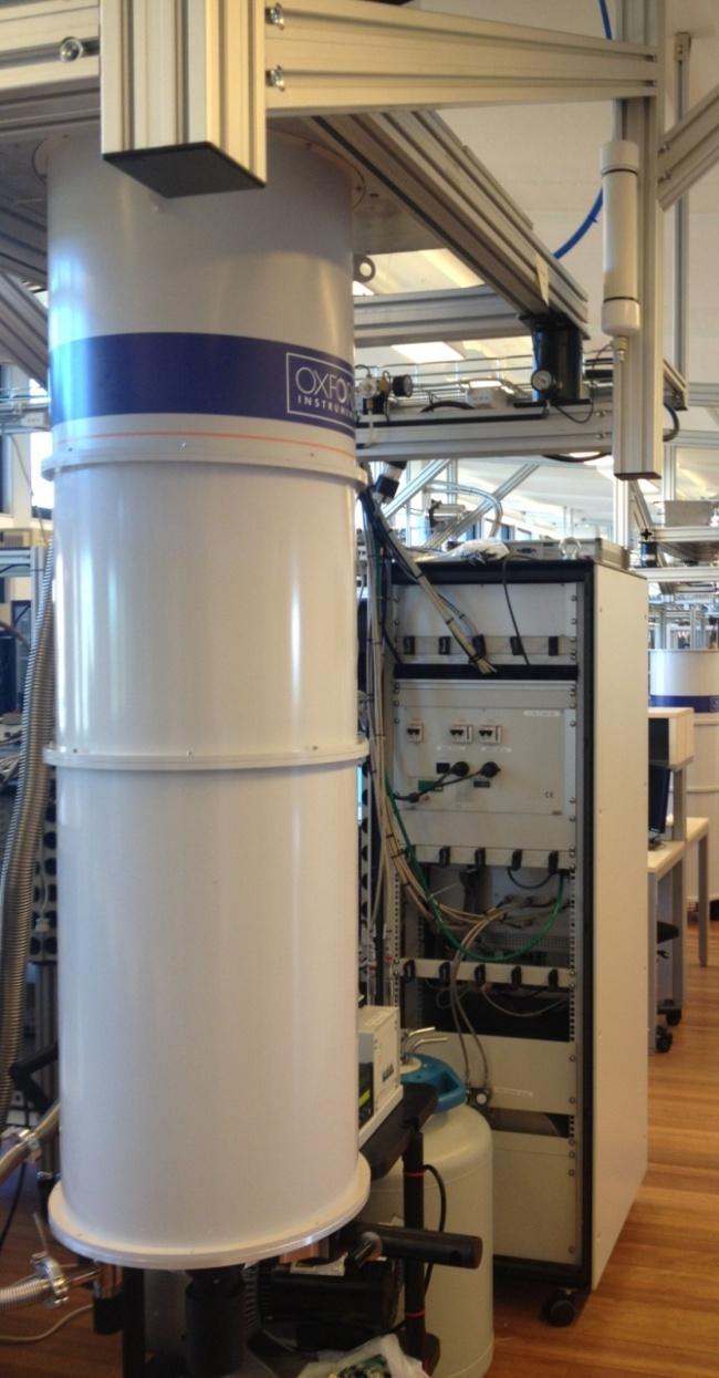
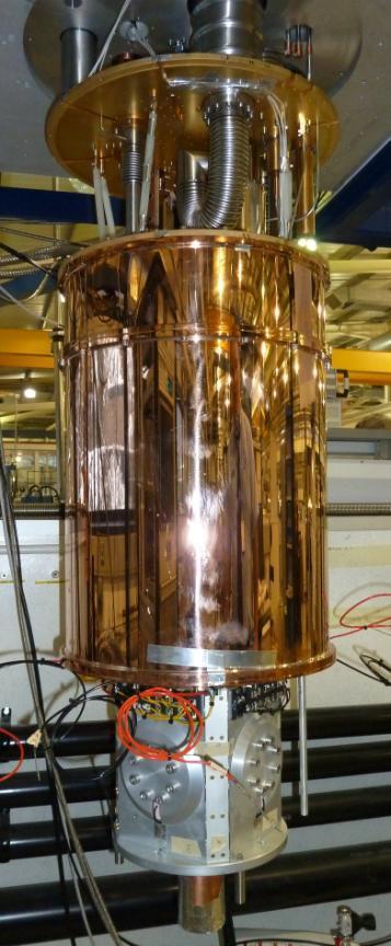
15 A key enabler for QT/QIP R&D: the Triton TM Cryofree dilution refrigerator platform QT device physics needs low (ultra-low) temperatures The initial, obvious advantage: no liquid cryogens No compromise on performance Base temperature <10 mk Cooling power up to 400 µw at 100 mk Attraction for QT science emerged: greatly enhanced sample space vs. wet 240 mm diameter mixing chamber plate Open structure for easy experimental access Ease of use Sample in vacuum with only a single room temperature O-ring seal (no IVC) Fully automatic cool-down from room temperature to base Remote control through TCP/IP protocol Page 15


16 What else is needed for QIP read/write control ULT plus Electrical Wide bandwidth electronics GHz pulse sequences Low noise amplification Low temperature filtering and amplification Low electron temperatures Magnetic Homogeneous fields Gradient fields 3D Vector fields AC fields Optical Low vibration HV/UHV fs pulse sequences Single photon emitters Optical windows Spectroscopic detectors Atomic UHV Gas injection Ion/electron beam Rapid scan SPM Page 16

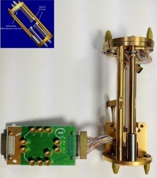
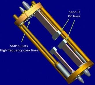
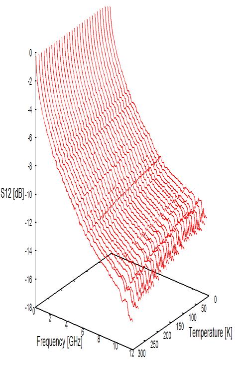
17 Triton DR: typical experimental services 4 K plate 2 off optical fibres 10 off UT-85 rigid coaxial cables 10 off S1 flexible coaxial cables 96 off dc lines Still plate 100 mk plate Mixing chamber plate, <10 mk Page 17
18 Experimental services, heat sinking and available cooling powers Fully loaded Triton DR: base temperature < 15 mk Page 18
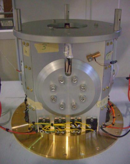
19 Triton DR integrated 3-axis superconducting magnets Page 19

20 Multiple Triton DR systems: Centre for Quantum Devices, Niels Bohr Institute, University of Copenhagen, Denmark Page 20


21 Multiple Triton DR systems: TU Delft, Netherlands Page 21


22 Fast throughput: top-loading sample exchange Page 22
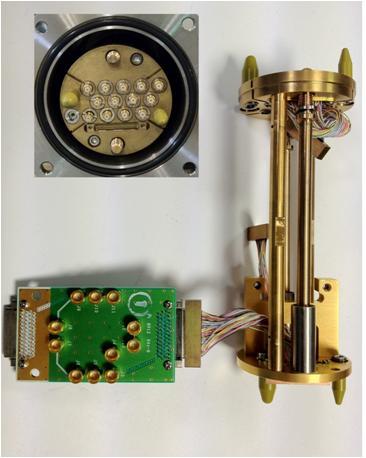
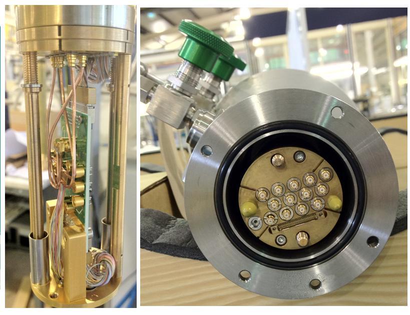
23 30 mm top-loading sample puck 4 off 18 GHz 25 off dc lines Page 23


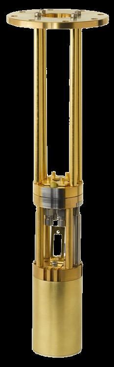
24 Fast throughput with larger sample space: bottom-loading sample exchange OVC break Sample puck Magnet Vacuum lock and gate valve Drive rods Page 24


25 70 mm bottom-loading sample puck 14 off 40 GHz 50 off dc lines < 8 hours cool-down time Page 25


26 Fast throughput with larger sample space: bottom-loading sample exchange MC plate Coaxes routed from MC plate to docking station Repeat connect/disconnect cycles Docking station Field centre Sample holder Page 26
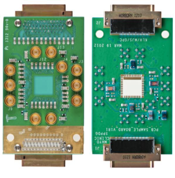
27 Sample instrumentation Page 27


28 New platform for yet greater capacity and capability: TritonXL 706 mm 1003 mm Ø 240 mm Ø 430 mm Page 28

29 TritonXL: sample space and wiring access Triton Ø 240 mm 1 x 50mm mm + 1 x 65 mm LoS ports TritonXL Ø 430 mm 6 x 50 mm + 1 x 100 mm LoS ports Page 29
30 And finally The future On-board cold electronics Filtering, multiplexing, amplifiers, Enhanced measurement Electron temperature thermometry Standardised measurement pucks Anticipating close participation in a number of QT Hubs For discussion! What are we not seeing yet in QC/QIP? What are we not seeing yet in QT beyond QC/QIP? Page 30
31 Thank you Page 31
Low Vibration Cryogenic Equipment
 PAGE 12 PAGE 13 ATTOCUBE S CRYOSTATS ATTODRY attodry1000....................... 14 cryogen-free cryostats with/without s attodry700.........................18 cryogen-free table-top cryostats with optical
Supplementary Information Our InGaN/GaN multiple quantum wells (MQWs) based one-dimensional (1D) grating structures
 based one-dimensional (1D) grating structures") Polarized white light from hybrid organic/iii-nitrides grating structures M. Athanasiou, R. M. Smith, S. Ghataora and T. Wang* Department of Electronic and Electrical Engineering, University of Sheffield,
Polarized white light from hybrid organic/iii-nitrides grating structures M. Athanasiou, R. M. Smith, S. Ghataora and T. Wang* Department of Electronic and Electrical Engineering, University of Sheffield,
Etching Capabilities at Harvard CNS. March 2008
 Etching Capabilities at Harvard CNS March 2008 CNS: A shared use facility for the Harvard Community and New England CNS Provides technical support, equipment and staff. Explicitly multi-disciplinary w/
SURFACE ENGINEERING MASS SPECTROMETERS FOR THIN FILMS, PLASMA AND SURFACE ENGINEERING
 SURFACE ENGINEERING MASS SPECTROMETERS FOR THIN FILMS, PLASMA AND SURFACE ENGINEERING HIDEN MS MASS SPECTROMETERS for Thin Films and Surface Engineering Hiden Analytical have been designing and developing
NNCI ETCH WORKSHOP - STANFORD NNCI PLASMA ETCH OVERVIEW. Usha Raghuram Stanford Nanofabrication Facility Stanford, CA May 24, 2016
 NNCI ETCH WORKSHOP - STANFORD NNCI PLASMA ETCH OVERVIEW Usha Raghuram Stanford Nanofabrication Facility Stanford, CA May 24, 2016 NNCI AT STANFORD Four labs under NNCI Umbrella at Stanford SNSF Stanford
Defining quality standards for the analysis of solid samples
 Defining quality standards for the analysis of solid samples Thermo Scientific Element GD Plus Glow Discharge Mass Spectrometer Redefine your quality standards for the elemental analysis of solid samples
Defining an optimal plasma processing toolkit for Indium Phosphide (InP) laser diode production
 laser diode production") White Paper Defining an optimal plasma processing toolkit for Indium Phosphide (InP) laser diode production The properties of InP which combine a wide band gap with high electron mobility, make it a desirable
White Paper Defining an optimal plasma processing toolkit for Indium Phosphide (InP) laser diode production The properties of InP which combine a wide band gap with high electron mobility, make it a desirable
Technology for Micro- and Nanostructures Micro- and Nanotechnology
 Lecture 10: Deposition Technology for Micro- and Nanostructures Micro- and Nanotechnology Peter Unger mailto: peter.unger @ uni-ulm.de Institute of Optoelectronics University of Ulm http://www.uni-ulm.de/opto
ALD & ALE Tutorial Speakers and Schedule
 ALD & ALE Tutorial Speakers and Schedule Sunday, July 29, 2018 1:00-1:05 Tutorial Welcome 1:05-1:50 1:50-2:35 2:35-3:20 Challenges of ALD Applications in Memory Semiconductor Devices, Choon Hwan Kim (SK
INTRODUCTION TO THE HYBRID PLASMA EQUIPMENT MODEL
 INTRODUCTION TO THE HYBRID PLASMA EQUIPMENT MODEL Prof. Mark J. Kushner Department of Electrical and Computer Engineering 1406 W. Green St. Urbana, IL 61801 217-144-5137 mjk@uiuc.edu http://uigelz.ece.uiuc.edu
Characteristics of Neutral Beam Generated by a Low Angle Reflection and Its Etch Characteristics by Halogen-Based Gases
 Characteristics of Neutral Beam Generated by a Low Angle Reflection and Its Etch Characteristics by Halogen-Based Gases Geun-Young Yeom SungKyunKwan University Problems of Current Etch Technology Scaling
2D MBE Activities in Sheffield. I. Farrer, J. Heffernan Electronic and Electrical Engineering The University of Sheffield
 2D MBE Activities in Sheffield I. Farrer, J. Heffernan Electronic and Electrical Engineering The University of Sheffield Outline Motivation Van der Waals crystals The Transition Metal Di-Chalcogenides
Instrumentation for sub-mm astronomy. Adam Woodcraft SUPA, University of Edinburgh
 Instrumentation for sub-mm astronomy Adam Woodcraft http://woodcraft.lowtemp.org SUPA, University of Edinburgh 1 2 Introduction Sub-mm astronomy 1 Astronomy at sub-mm wavelengths Between infrared and millimetre
Extrel is widely respected for the quality of mass spectrometer systems that are
 Extrel is widely respected for the quality of mass spectrometer systems that are available to the world's top research scientists. In response to increasing requests for complete turn-key systems built
ETCHING Chapter 10. Mask. Photoresist
 ETCHING Chapter 10 Mask Light Deposited Substrate Photoresist Etch mask deposition Photoresist application Exposure Development Etching Resist removal Etching of thin films and sometimes the silicon substrate
X- ray Photoelectron Spectroscopy and its application in phase- switching device study
 X- ray Photoelectron Spectroscopy and its application in phase- switching device study Xinyuan Wang A53073806 I. Background X- ray photoelectron spectroscopy is of great importance in modern chemical and
Which Optistat is right for you?
 OPTISTAT Optistat liquid cryogen optical cryostats for spectroscopy Which Optistat is right for you? Our easy to use, compact and efficient Optistat cryostats offer a wide range of options to suit most
Technical description of photoelectron spectrometer Escalab 250Xi
 Technical description of photoelectron spectrometer Escalab 250Xi Resource center Physical Methods of Surface Investigations 2014 Table of contents Common description 3 Analytical chamber 8 Preparation
Effect of Spiral Microwave Antenna Configuration on the Production of Nano-crystalline Film by Chemical Sputtering in ECR Plasma
 THE HARRIS SCIENCE REVIEW OF DOSHISHA UNIVERSITY, VOL. 56, No. 1 April 2015 Effect of Spiral Microwave Antenna Configuration on the Production of Nano-crystalline Film by Chemical Sputtering in ECR Plasma
Wafer-scale fabrication of graphene
 Wafer-scale fabrication of graphene Sten Vollebregt, MSc Delft University of Technology, Delft Institute of Mircosystems and Nanotechnology Delft University of Technology Challenge the future Delft University
Thermo Scientific ELEMENT GD PLUS Glow Discharge Mass Spectrometer. Defining quality standards for the analysis of solid samples
 Thermo Scientific ELEMENT GD PLUS Glow Discharge Mass Spectrometer Defining quality standards for the analysis of solid samples Redefine your quality standards for the elemental analysis of solid samples
Nano devices for single photon source and qubit
 Nano devices for single photon source and qubit, Acknowledgement K. Gloos, P. Utko, P. Lindelof Niels Bohr Institute, Denmark J. Toppari, K. Hansen, S. Paraoanu, J. Pekola University of Jyvaskyla, Finland
Supporting Online Material for
 www.sciencemag.org/cgi/content/full/327/5966/662/dc Supporting Online Material for 00-GHz Transistors from Wafer-Scale Epitaxial Graphene Y.-M. Lin,* C. Dimitrakopoulos, K. A. Jenkins, D. B. Farmer, H.-Y.
Ir TES electron-phonon thermal conductance and single photon detection
 Ir TES electron-phonon thermal conductance and single photon detection D. Bagliani, F. Gatti, M. Ribeiro Gomes, L. Parodi, L. Ferrari and R. Valle I.N.F.N. of Genoa, Via Dodecaneso, 33, 16146 Genova, Italy
Infrastructure of Thin Films Laboratory in Institute of Molecular Physics Polish Academy of Sciences
 Infrastructure of Thin Films Laboratory in Institute of Molecular Physics Polish Academy of Sciences Outline Sample preparation Magnetron sputtering Ion-beam sputtering Pulsed laser deposition Electron-beam
E SC 412 Nanotechnology: Materials, Infrastructure, and Safety Wook Jun Nam
 E SC 412 Nanotechnology: Materials, Infrastructure, and Safety Wook Jun Nam Lecture 10 Outline 1. Wet Etching/Vapor Phase Etching 2. Dry Etching DC/RF Plasma Plasma Reactors Materials/Gases Etching Parameters
There's Plenty of Room at the Bottom
 There's Plenty of Room at the Bottom 12/29/1959 Feynman asked why not put the entire Encyclopedia Britannica (24 volumes) on a pin head (requires atomic scale recording). He proposed to use electron microscope
Atomic Force/Magnetic Force Microscope
 Atomic Force/Magnetic Force Microscope Veeco Instruments Dimension 3000 SPM with Nanoscope IIIa controller Atomic Force Microscopy Mode Magnetic Force Microscopy Mode Vibration isolation and sound proof
Supplementary Methods A. Sample fabrication
 Supplementary Methods A. Sample fabrication Supplementary Figure 1(a) shows the SEM photograph of a typical sample, with three suspended graphene resonators in an array. The cross-section schematic is
Multialkali photocathodes grown by MBE technique. General Physics Institute, USSR, Academy of Sciences, , Moscow, Vavilov street, 38.
 Multialkali photocathodes grown by MBE technique Dubovoi l.a., Chernikov AS., Prokhorov A.M., Schelev M. Ya., Ushakov V. K. General Physics Institute, USSR, Academy of Sciences, 117942, Moscow, Vavilov
A DIVISION OF ULVAC-PHI
 A DIVISION OF ULVAC-PHI X-ray photoelectron spectroscopy (XPS/ESCA) is the most widely used surface analysis technique and has many well established industrial and research applications. XPS provides
Chapter 7 Plasma Basic
 Chapter 7 Plasma Basic Hong Xiao, Ph. D. hxiao89@hotmail.com www2.austin.cc.tx.us/hongxiao/book.htm Hong Xiao, Ph. D. www2.austin.cc.tx.us/hongxiao/book.htm 1 Objectives List at least three IC processes
Supporting Information
 Supporting Information Assembly and Densification of Nanowire Arrays via Shrinkage Jaehoon Bang, Jonghyun Choi, Fan Xia, Sun Sang Kwon, Ali Ashraf, Won Il Park, and SungWoo Nam*,, Department of Mechanical
FRAUNHOFER IISB STRUCTURE SIMULATION
 FRAUNHOFER IISB STRUCTURE SIMULATION Eberhard Bär eberhard.baer@iisb.fraunhofer.de Page 1 FRAUNHOFER IISB STRUCTURE SIMULATION Overview SiO 2 etching in a C 2 F 6 plasma Ga ion beam sputter etching Ionized
Repetition: Practical Aspects
 Repetition: Practical Aspects Reduction of the Cathode Dark Space! E x 0 Geometric limit of the extension of a sputter plant. Lowest distance between target and substrate V Cathode (Target/Source) - +
DEPOSITION OF THIN TiO 2 FILMS BY DC MAGNETRON SPUTTERING METHOD
 Chapter 4 DEPOSITION OF THIN TiO 2 FILMS BY DC MAGNETRON SPUTTERING METHOD 4.1 INTRODUCTION Sputter deposition process is another old technique being used in modern semiconductor industries. Sputtering
Hiden SIMS Secondary Ion Mass Spectrometers. Analysers for surface, elemental and molecular analysis
 Hiden SIMS Secondary Ion Mass Spectrometers Analysers for surface, elemental and molecular analysis vacuum analysis surface science plasma diagnostics gas analysis SIMS Versatility SIMS is a high sensitivity
Atomic Layer Deposition of Hafnium Oxide at Temperatures below 100ºC. K. C. Kragh
 Atomic Layer Deposition of Hafnium Oxide at Temperatures below 100ºC K. C. Kragh Dept. of Physics and Optical Engineering, Rose-Hulman Institute of Technology REU Student in the Advanced Materials Research
The Stanford Nanofabrication Facility. Etch Area Overview. May 21, 2013
 The Stanford Nanofabrication Facility Etch Area Overview May 21, 2013 High Density Plasma Systems Etcher Materials Etched Gases available Wafer Size Applied Materials P5000 MRIE ChA Applied Materials P5000
Graphene Fundamentals and Emergent Applications
 Graphene Fundamentals and Emergent Applications Jamie H. Warner Department of Materials University of Oxford Oxford, UK Franziska Schaffel Department of Materials University of Oxford Oxford, UK Alicja
Resistance Thermometry based Picowatt-Resolution Heat-Flow Calorimeter
 Resistance Thermometry based Picowatt-Resolution Heat-Flow Calorimeter S. Sadat 1, E. Meyhofer 1 and P. Reddy 1, 1 Department of Mechanical Engineering, University of Michigan, Ann Arbor, 48109 Department
VACUUM TECHNOLOGIES NEEDED FOR 3D DEVICE PROCESSING
 VACUUM TECHNOLOGIES NEEDED FOR 3D DEVICE PROCESSING Future ICs will use more 3D device structures such as finfets and gate-all-around (GAA) transistors, and so vacuum deposition processes are needed that
An environment designed for success
 An environment designed for success The nanofab is a centralized, open-access, training, service, and collaboration facility, focused on academic research and industrial applications in micro- and nanoscale
EE C245 ME C218 Introduction to MEMS Design Fall 2007
 EE C245 ME C218 Introduction to MEMS Design Fall 2007 Prof. Clark T.-C. Nguyen Dept. of Electrical Engineering & Computer Sciences University of California at Berkeley Berkeley, CA 94720 Lecture 5: ALD,
Chapter 7. Plasma Basics
 Chapter 7 Plasma Basics 2006/4/12 1 Objectives List at least three IC processes using plasma Name three important collisions in plasma Describe mean free path Explain how plasma enhance etch and CVD processes
Plasma-Surface Interactions in Patterning High-k k Dielectric Materials
 Plasma-Surface Interactions in Patterning High-k k Dielectric Materials October 11, 4 Feature Level Compensation and Control Seminar Jane P. Chang Department of Chemical Engineering University of California,
for XPS surface analysis
 Thermo Scientific Avantage XPS Software Powerful instrument operation and data processing for XPS surface analysis Avantage Software Atomic Concentration (%) 100 The premier software for surface analysis
EE143 Fall 2016 Microfabrication Technologies. Lecture 6: Thin Film Deposition Reading: Jaeger Chapter 6
 EE143 Fall 2016 Microfabrication Technologies Lecture 6: Thin Film Deposition Reading: Jaeger Chapter 6 Prof. Ming C. Wu wu@eecs.berkeley.edu 511 Sutardja Dai Hall (SDH) 1 Vacuum Basics Units 1 atmosphere
Principles of dilution refrigeration. A brief technology guide
 Principles of dilution refrigeration A brief technology guide 3 He 4 He About the authors Dr Graham Batey Chief Technical Engineer United Kingdom Graham completed his PhD in Low Temperature Physics at
Etching: Basic Terminology
 Lecture 7 Etching Etching: Basic Terminology Introduction : Etching of thin films and sometimes the silicon substrate are very common process steps. Usually selectivity, and directionality are the first
Low Temperature (LT), Ultra High Vacuum (UHV LT) Scanning Probe Microscopy (SPM) Laboratory
, Ultra High Vacuum (UHV LT) Scanning Probe Microscopy (SPM) Laboratory") Low Temperature (LT), Ultra High Vacuum (UHV LT) Scanning Probe Microscopy (SPM) Laboratory The laboratory of Low Temperature, Ultra High Vacuum (UHV LT) is specifically designed for surface science microscopy
Low Temperature (LT), Ultra High Vacuum (UHV LT) Scanning Probe Microscopy (SPM) Laboratory The laboratory of Low Temperature, Ultra High Vacuum (UHV LT) is specifically designed for surface science microscopy
Tutorial on Plasma Polymerization Deposition of Functionalized Films
 Tutorial on Plasma Polymerization Deposition of Functionalized Films A. Michelmore, D.A. Steele, J.D. Whittle, J.W. Bradley, R.D. Short University of South Australia Based upon review article RSC Advances,
3.155J/6.152J Microelectronic Processing Technology Fall Term, 2004
 3.155J/6.152J Microelectronic Processing Technology Fall Term, 2004 Bob O'Handley Martin Schmidt Quiz Nov. 17, 2004 Ion implantation, diffusion [15] 1. a) Two identical p-type Si wafers (N a = 10 17 cm
LECTURE 5 SUMMARY OF KEY IDEAS
 LECTURE 5 SUMMARY OF KEY IDEAS Etching is a processing step following lithography: it transfers a circuit image from the photoresist to materials form which devices are made or to hard masking or sacrificial
Thermo Scientific K-Alpha + XPS Spectrometer. Fast, powerful and accessible chemical analysis for surface and thin film characterization
 Thermo Scientific K-Alpha + XPS Spectrometer Fast, powerful and accessible chemical analysis for surface and thin film characterization X-ray Photoelectron Spectroscopy Quantitative, chemical identification
Modern Methods in Heterogeneous Catalysis Research: Preparation of Model Systems by Physical Methods
 Modern Methods in Heterogeneous Catalysis Research: Preparation of Model Systems by Physical Methods Methods for catalyst preparation Methods discussed in this lecture Physical vapour deposition - PLD
Institute for Electron Microscopy and Nanoanalysis Graz Centre for Electron Microscopy
 Institute for Electron Microscopy and Nanoanalysis Graz Centre for Electron Microscopy Micromechanics Ass.Prof. Priv.-Doz. DI Dr. Harald Plank a,b a Institute of Electron Microscopy and Nanoanalysis, Graz
Nanostructure. Materials Growth Characterization Fabrication. More see Waser, chapter 2
 Nanostructure Materials Growth Characterization Fabrication More see Waser, chapter 2 Materials growth - deposition deposition gas solid Physical Vapor Deposition Chemical Vapor Deposition Physical Vapor
The goal of this project is to enhance the power density and lowtemperature efficiency of solid oxide fuel cells (SOFC) manufactured by atomic layer
 manufactured by atomic layer") Stanford University Michael Shandalov1, Shriram Ramanathan2, Changhyun Ko2 and Paul McIntyre1 1Department of Materials Science and Engineering, Stanford University 2Division of Engineering and Applied
Stanford University Michael Shandalov1, Shriram Ramanathan2, Changhyun Ko2 and Paul McIntyre1 1Department of Materials Science and Engineering, Stanford University 2Division of Engineering and Applied
Surface Defects on Natural MoS 2
 Supporting Information: Surface Defects on Natural MoS 2 Rafik Addou 1*, Luigi Colombo 2, and Robert M. Wallace 1* 1 Department of Materials Science and Engineering, The University of Texas at Dallas,
Temperature control for Varian Cary line of UV/Vis Spectrophotometers and the Eclipse Fluorometer
 Temperature control for Varian Cary line of UV/Vis Spectrophotometers and the Eclipse Fluorometer Temperature Control without Compromise: rapid changes, precise temperatures, powerful complex functionality.
Etching Issues - Anisotropy. Dry Etching. Dry Etching Overview. Etching Issues - Selectivity
 Etching Issues - Anisotropy Dry Etching Dr. Bruce K. Gale Fundamentals of Micromachining BIOEN 6421 EL EN 5221 and 6221 ME EN 5960 and 6960 Isotropic etchants etch at the same rate in every direction mask
Brigham Young University. Infiltration of CNT-M Microstructures using CVD and ALD Presented by: Collin Brown, Jason Kyle Anderson
 Infiltration of CNT-M Microstructures using CVD and ALD Presented by: Collin Brown, Jason Kyle Anderson October 31st, 2013 Acknowledgments Jason Kyle Anderson for his help in getting the system to work
Application of the GD-Profiler 2 to the PV domain
 Application of the GD-Profiler 2 to the PV domain GD Profiler 2 RF GDOES permits to follow the distribution of the elements as function of depth. This is an ultra fast characterisation technique capable
MICROCHIP MANUFACTURING by S. Wolf
 by S. Wolf Chapter 15 ALUMINUM THIN-FILMS and SPUTTER-DEPOSITION 2004 by LATTICE PRESS CHAPTER 15 - CONTENTS Aluminum Thin-Films Sputter-Deposition Process Steps Physics of Sputter-Deposition Magnetron-Sputtering
A TES Bolometer for THz FT-Spectroscopy
 A TES Bolometer for THz FT-Spectroscopy M. Kehrt, J. Beyer, C. Monte, J. Hollandt Physikalisch-Technische Bundesanstalt Abbestraße 2-12, Berlin, Germany E-Mail: Mathias.Kehrt@PTB.de Abstract - We recently
A novel sputtering technique: Inductively Coupled Impulse Sputtering (ICIS)
") IOP Conference Series: Materials Science and Engineering A novel sputtering technique: Inductively Coupled Impulse Sputtering (ICIS) To cite this article: D A L Loch and A P Ehiasarian 2012 IOP Conf. Ser.:
IOP Conference Series: Materials Science and Engineering A novel sputtering technique: Inductively Coupled Impulse Sputtering (ICIS) To cite this article: D A L Loch and A P Ehiasarian 2012 IOP Conf. Ser.:
Thin Film Deposition
 Thin Film Deposition Name Picture Description Site Responsible 1 MODA Surface Analysis Chamber The MODA surface Analysis chamber is equipped with several experimental techniques aimed to the study of the
Instrumentation and Operation
 Instrumentation and Operation 1 STM Instrumentation COMPONENTS sharp metal tip scanning system and control electronics feedback electronics (keeps tunneling current constant) image processing system data
Cover Page. The handle holds various files of this Leiden University dissertation
 Cover Page The handle http://hdl.handle.net/1887/38444 holds various files of this Leiden University dissertation Author: Haan, Arthur den Title: Nuclear magnetic resonance force microscopy at millikelvin
PHYSICS PAST PAPERS PHYSICS PAPER Suppose the handle bars of the wheelbarrow in question 2 were extended, which force(s) would
 would") PHYSICS PAST PAPERS PHYSICS PAPER 1 1995 1. Name the instrument that would be most suitable for measuring the thickest of one sheet of this question paper. Figure 1 shows a worker ready to lift a load
PHYSICS PAST PAPERS PHYSICS PAPER 1 1995 1. Name the instrument that would be most suitable for measuring the thickest of one sheet of this question paper. Figure 1 shows a worker ready to lift a load
Outlines 3/12/2011. Vacuum Chamber. Inside the sample chamber. Nano-manipulator. Focused ion beam instrument. 1. Other components of FIB instrument
 Focused ion beam instruments Outlines 1. Other components of FIB instrument 1.a Vacuum chamber 1.b Nanomanipulator 1.c Gas supply for deposition 1.d Detectors 2. Capabilities of FIB instrument Lee Chow
MoBiKID Kinetic Inductance Detectors for up-coming B-mode satellite experiments
 MoBiKID Kinetic Inductance Detectors for up-coming B-mode satellite experiments TIPP 17 - BEIJING INFN, Sezione di Roma Dawn of the universe: where are we? Looking into the CMB for a proof of the Inflation...
Gold Nanoparticles Floating Gate MISFET for Non-Volatile Memory Applications
 Gold Nanoparticles Floating Gate MISFET for Non-Volatile Memory Applications D. Tsoukalas, S. Kolliopoulou, P. Dimitrakis, P. Normand Institute of Microelectronics, NCSR Demokritos, Athens, Greece S. Paul,
Evaluation of the plasmaless gaseous etching process
 Solid State Phenomena Vol. 134 (28) pp 7-1 Online available since 27/Nov/2 at www.scientific.net (28) Trans Tech Publications, Switzerland doi:1.428/www.scientific.net/ssp.134.7 Evaluation of the plasmaless
System design of 60K Stirling-type co-axial pulse tube coolers for HTS RF filters
 System design of 60K Stirling-type co-axial pulse tube coolers for HTS RF filters Y. L. Ju, K. Yuan, Y. K. Hou, W. Jing, J. T. Liang and Y. Zhou Cryogenic Laboratory, Technical Institute of Physics and
Local spectroscopy. N. Witkowski W. Sacks
 Local spectroscopy N. Witkowski W. Sacks Outlook 1. STM/STS theory elements a. history of STM and basic idea b. tunnel effect c. STM/STS 2. Technology a. STM design : vibration and thermal drift b. STM
Dynamization evolution of Dry Etch Tools in Semiconductor Device Fabrication Gordon Cameron Intel Corp (November 2005)
") Dynamization evolution of Dry Etch Tools in Semiconductor Device Fabrication Gordon Cameron Intel Corp (November 2005) Abstract Engineering Systems follow recognized trends of evolution; the main parameters
Dynamization evolution of Dry Etch Tools in Semiconductor Device Fabrication Gordon Cameron Intel Corp (November 2005) Abstract Engineering Systems follow recognized trends of evolution; the main parameters
CHEMICAL VAPOR DEPOSITION (CVD)
") CHEMICAL VAPOR DEPOSITION (CVD) A process of formation of a non-volatile solid film on a substrate from the reaction of vapor phase chemical reactants containing the right proportion of constituents. ELEMETRY
CHEMICAL VAPOR DEPOSITION (CVD) A process of formation of a non-volatile solid film on a substrate from the reaction of vapor phase chemical reactants containing the right proportion of constituents. ELEMETRY
Keywords. 1=magnetron sputtering, 2= rotatable cathodes, 3=substrate temperature, 4=anode. Abstract
 Managing Anode Effects and Substrate Heating from Rotatable Sputter Targets. F. Papa*, V. Bellido-Gonzalez**, Alex Azzopardi**, Dr. Dermot Monaghan**, *Gencoa Technical & Business Support in US, Davis,
Competitive Advantages of Ontos7 Atmospheric Plasma
 Competitive Advantages of Ontos7 Atmospheric Plasma Eric Schulte Matt Phillips Keith Cooper SETNA Proprietary 1 Advantages of Ontos7 Atmospheric Plasma Process over Vacuum RIE Plasma for Die/Wafer Surface
Vacuum Kelvin Force Probe Research Richard Williams August 1st 2008
 Vacuum Kelvin Force Probe Research Richard Williams August 1st 2008 Introduction Kelvin Force Probe Microscopy is an analytical method to measure the contact potential difference between a reference material
XPS & Scanning Auger Principles & Examples
 XPS & Scanning Auger Principles & Examples Shared Research Facilities Lunch Talk Contact info: dhu Pujari & Han Zuilhof Lab of rganic Chemistry Wageningen University E-mail: dharam.pujari@wur.nl Han.Zuilhof@wur.nl
Manufacture of Nanostructures for Power Electronics Applications
 Manufacture of Nanostructures for Power Electronics Applications Brian Hunt and Jon Lai Etamota Corporation 2672 E. Walnut St. Pasadena, CA 91107 APEC, Palm Springs Feb. 23rd, 2010 1 Background Outline
XBC300 Gen2. Fully-automated debonder and Cleaner
 XBC300 Gen2 Fully-automated debonder and Cleaner XBC300 Gen2 FULLY AUTOMATED DEBONDER AND CLEANER The SUSS XBC300 Gen2 debonder and cleaner platform is designed for process development as well as high
Microscopy Cryostat System
 OF AMERICA, INC. Microscopy Cryostat System RC102-CFM Microscopy Cryostat offers fast cooldown, high efficiency, lowest thermal drift, excellent temperature stability and ultra low vibration Optical cryostat
Kavli Workshop for Journalists. June 13th, CNF Cleanroom Activities
 Kavli Workshop for Journalists June 13th, 2007 CNF Cleanroom Activities Seeing nm-sized Objects with an SEM Lab experience: Scanning Electron Microscopy Equipment: Zeiss Supra 55VP Scanning electron microscopes
Plasma Deposition (Overview) Lecture 1
 Lecture 1") Plasma Deposition (Overview) Lecture 1 Material Processes Plasma Processing Plasma-assisted Deposition Implantation Surface Modification Development of Plasma-based processing Microelectronics needs (fabrication
Plasma Deposition (Overview) Lecture 1 Material Processes Plasma Processing Plasma-assisted Deposition Implantation Surface Modification Development of Plasma-based processing Microelectronics needs (fabrication
EE 527 MICROFABRICATION. Lecture 24 Tai-Chang Chen University of Washington
 EE 527 MICROFABRICATION Lecture 24 Tai-Chang Chen University of Washington EDP ETCHING OF SILICON - 1 Ethylene Diamine Pyrocatechol Anisotropy: (100):(111) ~ 35:1 EDP is very corrosive, very carcinogenic,
Product Overview. Ultimate NanoScience. Combined Scanning Probe Microscopy, Electron Spectroscopy and Thin-Film technology from a single supplier
 Ultimate NanoScience Product Overview Combined Scanning Probe Microscopy, Electron Spectroscopy and Thin-Film technology from a single supplier o th d t c ti c t ch ppo t d o p od ct More than 1100 man-years
UHF-ECR Plasma Etching System for Dielectric Films of Next-generation Semiconductor Devices
 UHF-ECR Plasma Etching System for Dielectric Films of Next-generation Semiconductor Devices 1 UHF-ECR Plasma Etching System for Dielectric Films of Next-generation Semiconductor Devices Katsuya Watanabe
Fundamental insight into ALD processing by in-
 Fakultät Elektrotechnik und Informationstechnik Institut für Halbleiter- und Mikrosystemtechnik Fundamental insight into ALD processing by in- situ observation Johann W. Bartha M. Albert, M. Junige and
2D Materials Research Activities at the NEST lab in Pisa, Italy. Stefan Heun NEST, Istituto Nanoscienze-CNR and Scuola Normale Superiore, Pisa, Italy
 2D Materials Research Activities at the NEST lab in Pisa, Italy Stefan Heun NEST, Istituto Nanoscienze-CNR and Scuola Normale Superiore, Pisa, Italy 2D Materials Research Activities at the NEST lab in
CHARACTERIZING PROCESS SEMICONDUCTOR THIN FILMS WITH A CONFOCAL MICRO X-RAY FLUORESCENCE MICROSCOPE
 CHARACTERIZING PROCESS SEMICONDUCTOR THIN FILMS WITH A CONFOCAL MICRO X-RAY FLUORESCENCE MICROSCOPE 218 Chris M. Sparks 1, Elizabeth P. Hastings 2, George J. Havrilla 2, and Michael Beckstead 2 1. ATDF,
Beetle UHV VT AFM / STM
 UHV VT AFM / STM RHK Technology Imaging the Future of Nanoscience UHV VT AFM / STM Engineered Excellence Everyday, in university and government labs around the globe, RHK research platforms lead to new
Case Study of Electronic Materials Packaging with Poor Metal Adhesion and the Process for Performing Root Cause Failure Analysis
 Case Study of Electronic Materials Packaging with Poor Metal Adhesion and the Process for Performing Root Cause Failure Analysis Dr. E. A. Leone BACKGRUND ne trend in the electronic packaging industry
HELIX SFT. Static Vacuum ARGUS VI HELIX SFT. Static Vacuum Mass Spectrometer Static Vacuum Mass Spectrometer
 ARGUS VI HELIX SFT Static Vacuum Mass Spectrometer Static Vacuum Mass Spectrometer Static Vacuum HELIX SFT Low Volume Multicollection High Mass Resolution 3 Based on more than 20 years of experience in
UNIT 3. By: Ajay Kumar Gautam Asst. Prof. Dev Bhoomi Institute of Technology & Engineering, Dehradun
 UNIT 3 By: Ajay Kumar Gautam Asst. Prof. Dev Bhoomi Institute of Technology & Engineering, Dehradun 1 Syllabus Lithography: photolithography and pattern transfer, Optical and non optical lithography, electron,
EE 527 MICROFABRICATION. Lecture 25 Tai-Chang Chen University of Washington
 EE 527 MICROFABRICATION Lecture 25 Tai-Chang Chen University of Washington ION MILLING SYSTEM Kaufmann source Use e-beam to strike plasma A magnetic field applied to increase ion density Drawback Low etch
GHZ ELECTRICAL PROPERTIES OF CARBON NANOTUBES ON SILICON DIOXIDE MICRO BRIDGES
 GHZ ELECTRICAL PROPERTIES OF CARBON NANOTUBES ON SILICON DIOXIDE MICRO BRIDGES SHENG F. YEN 1, HAROON LAIS 1, ZHEN YU 1, SHENGDONG LI 1, WILLIAM C. TANG 1,2, AND PETER J. BURKE 1,2 1 Electrical Engineering