The Stanford Nanofabrication Facility. Etch Area Overview. May 21, 2013
|
|
|
- Leon Bennett
- 5 years ago
- Views:
Transcription
1 The Stanford Nanofabrication Facility Etch Area Overview May 21, 2013
2 High Density Plasma Systems Etcher Materials Etched Gases available Wafer Size Applied Materials P5000 MRIE ChA Applied Materials P5000 MRIE ChB Applied Materials P5000 MRIE ChC Lam 9400 TCP Plasmatherm Versaline ICP Plasmatherm Versaline ICP PlasmaQuest 100 ECR Al/Si SiO2, SiN Poly Si, Si Ar, BCl3, CF4, Cl2, N2, Ar CHF3,CF4, Ar, He, O2 N2 Cl2, HBr, NF3, CF4, SF6, He/O2 O2, N2, H2, Cl2, HBr, PolySi, Si CF4, C2F6 varied metals Cl2, BCl3, O2, SF6, Ar, CF4, CH4, N2 Ox, SiN C4F8, H2, Ar, CF4, O2, CHF3, He, N2 Varied Ar, SF6, N2, H2, O2, CF4, He, BCl3, Cl2 4 in 4 in 4 in Maximum Load Size 8 per loadlock pumpdown, 50 max 8 per loadlock pumpdown, 50 max 8 per loadlock pumpdown, 50 max Cleanliness Back End MOS Back End MOS Front End MOS 4 25 Front End MOS 4in (6 in*) 4 in (6 in*) 1 1 Flexible (All Classes*) Flexible (All Classes*) 4 in 1 Flexible Oxford PlasmaPro 100 Cobra GaAs, III V, II VI BCl3, SF6, CL2, O2, HBr, H2, Ar, N2, CH4 4 in 1 Flexible
3 Silicon DRIE and RIE Etcher Materials Etched Gases Wafer Size PlasmaTherm Versaline DSE Si SF6, C4F8, O2, Ar 4 in (6 *) Maximum Load Size 1 Cleanliness Flexible (All Classes*) STS Si SF6, C4F8, O2 4 in 1 Back End MOS STS HRM Si SF6, C4F8, O2 4 in 1 Back End MOS Etcher Materials Etched Gases available Wafer Size Maximum Load Size Cleanliness Applied Materials 8100 SiO2, SiN, Si, PR O2, CHF3, SF6, Ar, NF3 4 in 24 Back End MOS Drytek 100 Drytek 100 (Modified) PolySi, Si, SiN, PR Varied O2, CF4, SF6, CHClF2 O2, N2, Ar, SF6, CHF3, C2F6, C4F8 2 6 in, pieces 6 4Slots Front End 2 Slots Flexible 2 6 in, pieces 1 Flexible
4 Ashers and Dry Chemical Etching Etcher Materials Etched Gases available Wafer Size Maximum Load Size Cleanliness Gasonics Asher PR ashing O2 4 in 25 Front End MOS Matrix Asher PR ashing O2 4 in 25 Flexible Etcher Materials Etched Gases available Wafer Size Maximum Load Size Cleanliness Xactix Si, Ge, SiGe XeF2, N2 Pieces to 6 1 Flexible HF Vapor Etch 1 SiO2 HF acid Pieces to 6 1 Front End MOS HF Vapor Etch 2 SiO2 HF acid Pieces to 6 1 Flexible SPTS Micro Etch HF Vapor** SiO2 Hydrogen Fluoride Pieces to 6 1 All Classes Tousimis Critical Point Dryer NA CO2 Pieces to 6 1 All Classes


5 PlasmaTherm DSE ICP II DSE 3 Turn Source RF PKG: 3.5kW*, 2MHz RF 100W, 1kHz 100kHz DBS (Digital Bias Supply) Electrode Chiller temp 40 C 40 C Fast gas switching Optical Endpoint Detection Mechanical Clamp
 <2.5 Scallop Depth (um) <1.")
6 PlasmaTherm DSE Parameter Etch rate (um/min) Specs Selectivity Si:PR >100:1 >10 for 100 micron trench Profile Angle 90 degrees +/ 2 Scallop Length (um) <2.5 Scallop Depth (um) <1.0 %Nonunifomity (6 mm edge exclusion) Run to run %Nonuniformity <3% 2.00%
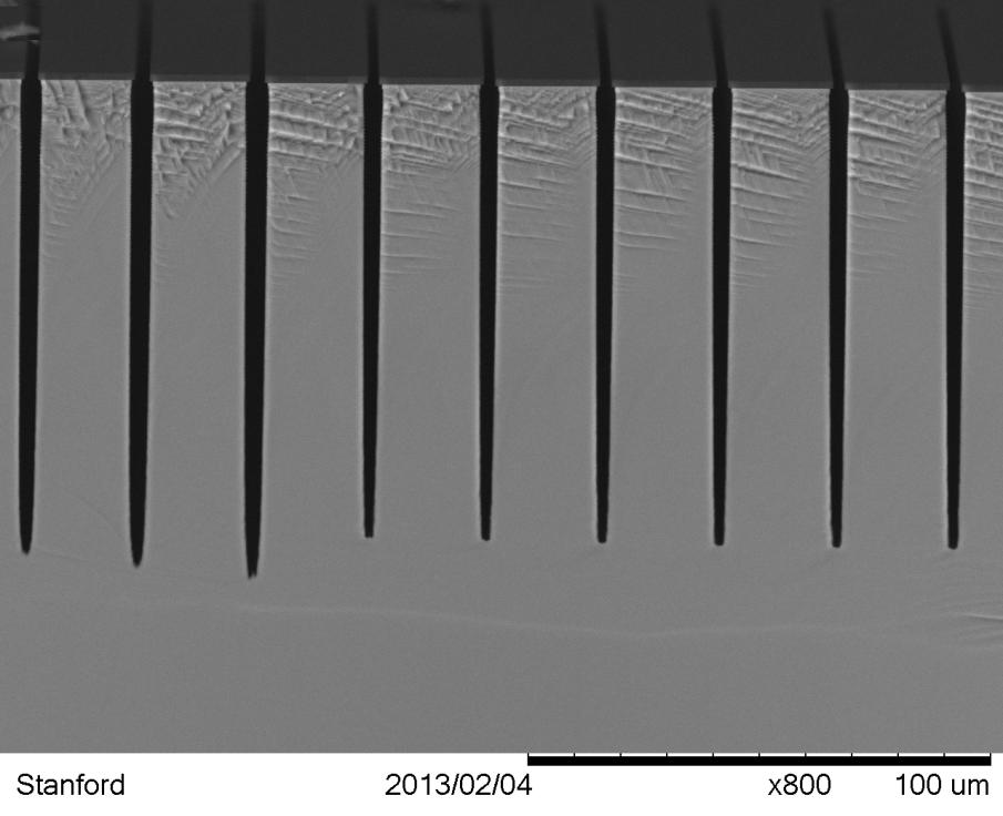
7 PlasmaTherm DSE

8 PlasmaTherm Versaline Metal Etcher
9 Plasmatherm Versaline Metal Etcher Mechanical clamp Electrode Temp 10C 60 C ICP Source: 2.5 KHz, 2.5KW RF Bias: MHZ, 300 W Heated chamber liners Laser endpoint system Optical endpoint detection system Gases: Cl2, BCl3, O2, SF6, Ar, CF4, CH4, N2 Parameter Recent Monitor (6 wafer) Al Etch Rate 6208 A/min (10.7%) Oxide Etch rate Photoresist Etch Rate Al:Pr Selectivity Al:Oxide Selecivity 964 A/min (6.85%) 4727 A/min (11.9%)
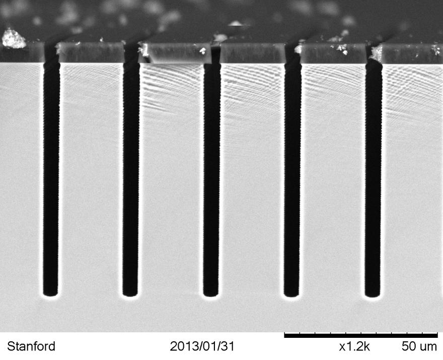
10 PlasmaTherm Versaline Oxide Etcher Mechanical clamp Electrode Temp 40 C 40 C ICP Source: 2.5 KHz, 2.5KW RF Bias: MHZ, 300 W Heated chamber liners Laser endpoint system Optical endpoint detection system Gases: C4F8, H2, Ar, CF4, O2, CHF3, He, N2 Parameter Spec Etch Rate A/min >2500 Selectivity Oxide/PR >1:1 Within Wfr %Nonuniformity Wafer to wafer %Nonuniformity <3% <3%

11 PlasmaTherm Versaline Oxide Etcher Parameter Unit Light Etch Process Time s 5 54 Pressure mtorr 5 5 CHF3 sccm ICP Power W Bias Power W Electrode C Temperature Lid Temperature C Liner C Temperature Spool Temperature C SiO2 film etched using metal mask, showing high fidelity pattern transfer and good sidewall smoothness and verticality. The etch rate was 110 nm/min, and selectivity to photoresist was about 3:1.


12 Oxford PlasmaPro 100 Cobra Materials: GaAs, II VI Mechanical Clamp Electrode Temp = 150 C 400 C 2 MHz 3KW/600 W MHz Laser interferometer Gases: BCl3, SF6, CL2, O2, HBr, H2, Ar, N2, CH4 Wafer: GaAs substrate > 1um AlGaAs sacrificial layer > 164nm GaAs top membrane Lithography: pattern written in ZEP (~300nm thick) using JEOL e beam writer Structures: photonic crystal cavities on suspended membranes


13 Applied Materials AMT 8100 Materials: Si, SiO2, Ge, SiGe, PR Gases: CHF3, SF6, NF3, Ar, O2 Electrode: Hexode, Ardel clamp, no He, 20 C Load: 24 wafers Cleanliness: Backend MOS 1982 vintage, workhorse, used by electronics researchers


14 Drytek 2/4 Materials: Poly Si, Si, SiN, PR Gases: ChClF2, CF4, SF6, O2 Electrode: 6 electrodes, no clamp, 20 C Load: 6wafers Cleanliness: 4 Frontend, 2 Flexible 1982 vintage, workhorse, fast, easy Materials: Poly, Si, SiN, SiO2, W, Ti Gases: CHF3, SF6, C2F6, C4F8, O2, N2, Ar Electrode: 1 electrode, 20 C Load: 1 wafer up to 6 Cleanliness: Flexible Flexible, easy, no clamping

 Load:")

15 Materials: PolySi, Si, SiC Gases: Cl2, HBr, SF6, Oe, He, CF4 Electrode: 4, He clamping, 0 C 90 C (operates at 60 C) Load: cassette to cassette Cleanliness: Front End MOS Vintage 1994, classic version Lam 9400

16 MRC Materials: Si, SiO2, Ge, SiGe, PR Gases: CHF3, SF6, CF4, Ar, O2 Electrode: No Clamp, 7 electrode, 20 C Load: 1 at a time Cleanliness: Flexible Low pressure system, most often used for Ar sputtering Easy, fast, flexible

17 PQuest Materials: Anything goes, III V Gases: Ar, SF6, N2, H2, O2, CF4, He, BCl3, Cl2 Electrode: He clamp, 0 C 200 C Load: single 4 wafer Cleanliness: Flexible ECR, circa 1980 Mostly used for III V and other flexible processes Wet clean between chlorine and fluorine etch weeks

18 STS Multiplex Pro HRM Materials: Si Gases: Bosch Electrode: 4, He Clamp, ~40C Load: Single wafer Cleanliness: Backend MOS Resist burns easily, prototype system
, custom wafer")
19 STS ASE Materials: Si Gases: Bosch Electrode: 4, He Clamp, ~35C Load: Single wafer Cleanliness: Backend MOS Slow etch (2 um/min), custom wafer holder.
20 Future for SNF Etch Tools Near term: Migrate towards common repairable spares wherever possible (pumps, chillers, MFC s, baratrons) Develop backup strategy for vulnerable hard drives Address process gas cylinder management Mid term: Expand cleanliness definitions beyond the traditional three classes Upgrade process gas cabinets Long term: Migrate to 6 /8 compatible tools (removing aging tools) Migrate towards common tools
21 Cleanliness/Contamination in Dry Etching
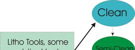
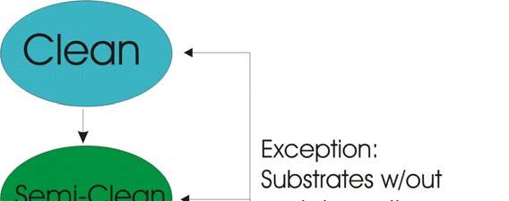
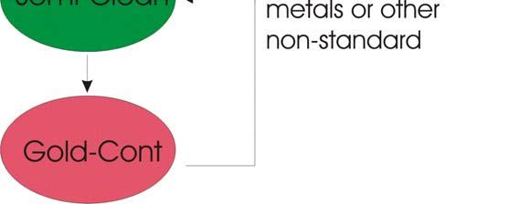
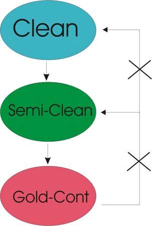
22 Cleanliness/Contamination in Dry Etching Motivation: Electronics is last century (last millenium?) More demand for non traditional materials New materials of electronics Optics demands New materials constraints Electronics needs voltage shift concerns Detector needs Lifetime concerns Question: How to quantify? Concerns for etchers Mechanism of contamination transfer How to set up barriers to transfer
23 Cleanliness/Contamination in Dry Etching Trace Underlying stop film Gold Cont Film Etched Mask Material Protected film
NNCI ETCH WORKSHOP - STANFORD NNCI PLASMA ETCH OVERVIEW. Usha Raghuram Stanford Nanofabrication Facility Stanford, CA May 24, 2016
 NNCI ETCH WORKSHOP - STANFORD NNCI PLASMA ETCH OVERVIEW Usha Raghuram Stanford Nanofabrication Facility Stanford, CA May 24, 2016 NNCI AT STANFORD Four labs under NNCI Umbrella at Stanford SNSF Stanford
Etching Capabilities at Harvard CNS. March 2008
 Etching Capabilities at Harvard CNS March 2008 CNS: A shared use facility for the Harvard Community and New England CNS Provides technical support, equipment and staff. Explicitly multi-disciplinary w/
NNCI Dry Etch Capabilities
 NNCI Site Tool Type Gases Application Wafer size Cornell Plasmatherm SF6, C4F8, O2, Ar Deep silicon etch 100mm Versaline ICP Deep Ge etch DSEIII SOI Cornell Unaxis 770 ICP SF6, C4F8, O2, Ar Deep silicon
Etching Issues - Anisotropy. Dry Etching. Dry Etching Overview. Etching Issues - Selectivity
 Etching Issues - Anisotropy Dry Etching Dr. Bruce K. Gale Fundamentals of Micromachining BIOEN 6421 EL EN 5221 and 6221 ME EN 5960 and 6960 Isotropic etchants etch at the same rate in every direction mask
ETCHING Chapter 10. Mask. Photoresist
 ETCHING Chapter 10 Mask Light Deposited Substrate Photoresist Etch mask deposition Photoresist application Exposure Development Etching Resist removal Etching of thin films and sometimes the silicon substrate
E SC 412 Nanotechnology: Materials, Infrastructure, and Safety Wook Jun Nam
 E SC 412 Nanotechnology: Materials, Infrastructure, and Safety Wook Jun Nam Lecture 10 Outline 1. Wet Etching/Vapor Phase Etching 2. Dry Etching DC/RF Plasma Plasma Reactors Materials/Gases Etching Parameters
Etching: Basic Terminology
 Lecture 7 Etching Etching: Basic Terminology Introduction : Etching of thin films and sometimes the silicon substrate are very common process steps. Usually selectivity, and directionality are the first
Section 3: Etching. Jaeger Chapter 2 Reader
 Section 3: Etching Jaeger Chapter 2 Reader Etch rate Etch Process - Figures of Merit Etch rate uniformity Selectivity Anisotropy d m Bias and anisotropy etching mask h f substrate d f d m substrate d f
Reactive Ion Etching (RIE)
") Reactive Ion Etching (RIE) RF 13.56 ~ MHz plasma Parallel-Plate Reactor wafers Sputtering Plasma generates (1) Ions (2) Activated neutrals Enhance chemical reaction 1 2 Remote Plasma Reactors Plasma Sources
Reactive Ion Etching (RIE) RF 13.56 ~ MHz plasma Parallel-Plate Reactor wafers Sputtering Plasma generates (1) Ions (2) Activated neutrals Enhance chemical reaction 1 2 Remote Plasma Reactors Plasma Sources
Regents of the University of California
 Deep Reactive-Ion Etching (DRIE) DRIE Issues: Etch Rate Variance The Bosch process: Inductively-coupled plasma Etch Rate: 1.5-4 μm/min Two main cycles in the etch: Etch cycle (5-15 s): SF 6 (SF x+ ) etches
EE 527 MICROFABRICATION. Lecture 25 Tai-Chang Chen University of Washington
 EE 527 MICROFABRICATION Lecture 25 Tai-Chang Chen University of Washington ION MILLING SYSTEM Kaufmann source Use e-beam to strike plasma A magnetic field applied to increase ion density Drawback Low etch
EE C245 ME C218 Introduction to MEMS Design Fall 2007
 EE C245 ME C218 Introduction to MEMS Design Fall 2007 Prof. Clark T.-C. Nguyen Dept. of Electrical Engineering & Computer Sciences University of California at Berkeley Berkeley, CA 94720 Lecture 12: Mechanics
4FNJDPOEVDUPS 'BCSJDBUJPO &UDI
 2010.5.4 1 Major Fabrication Steps in CMOS Process Flow UV light oxygen Silicon dioxide Silicon substrate Oxidation (Field oxide) photoresist Photoresist Coating Mask exposed photoresist Mask-Wafer Exposed
Lecture 15 Etching. Chapters 15 & 16 Wolf and Tauber. ECE611 / CHE611 Electronic Materials Processing Fall John Labram 1/76
 Lecture 15 Etching Chapters 15 & 16 Wolf and Tauber 1/76 Announcements Term Paper: You are expected to produce a 4-5 page term paper on a selected topic (from a list). Term paper contributes 25% of course
Plasma etch control by means of physical plasma parameter measurement with HERCULES Sematech AEC/APC Symposium X
 Plasma etch control by means of physical plasma parameter measurement with HERCULES A. Steinbach F. Bell D. Knobloch S. Wurm Ch. Koelbl D. Köhler -1- Contents - Introduction - Motivation - Plasma monitoring
Characteristics of Neutral Beam Generated by a Low Angle Reflection and Its Etch Characteristics by Halogen-Based Gases
 Characteristics of Neutral Beam Generated by a Low Angle Reflection and Its Etch Characteristics by Halogen-Based Gases Geun-Young Yeom SungKyunKwan University Problems of Current Etch Technology Scaling
Device Fabrication: Etch
 Device Fabrication: Etch 1 Objectives Upon finishing this course, you should able to: Familiar with etch terminology Compare wet and dry etch processes processing and list the main dry etch etchants Become
Dry Etching Zheng Yang ERF 3017, MW 5:15-6:00 pm
 Dry Etching Zheng Yang ERF 3017, email: yangzhen@uic.edu, MW 5:15-6:00 pm Page 1 Page 2 Dry Etching Why dry etching? - WE is limited to pattern sizes above 3mm - WE is isotropic causing underetching -
EE 527 MICROFABRICATION. Lecture 24 Tai-Chang Chen University of Washington
 EE 527 MICROFABRICATION Lecture 24 Tai-Chang Chen University of Washington EDP ETCHING OF SILICON - 1 Ethylene Diamine Pyrocatechol Anisotropy: (100):(111) ~ 35:1 EDP is very corrosive, very carcinogenic,
CHAPTER 6: Etching. Chapter 6 1
 Chapter 6 1 CHAPTER 6: Etching Different etching processes are selected depending upon the particular material to be removed. As shown in Figure 6.1, wet chemical processes result in isotropic etching
Advances in Back-side Via Etching of SiC for GaN Device Applications
 Advances in Back-side Via Etching of SiC for GaN Device Applications Anthony Barker, Kevin Riddell, Huma Ashraf & Dave Thomas SPTS Technologies, Ringland Way, Newport NP18 2TA, UK, dave.thomas@spts.com,
3.155J/6.152J Microelectronic Processing Technology Fall Term, 2004
 3.155J/6.152J Microelectronic Processing Technology Fall Term, 2004 Bob O'Handley Martin Schmidt Quiz Nov. 17, 2004 Ion implantation, diffusion [15] 1. a) Two identical p-type Si wafers (N a = 10 17 cm
Lecture 6 Plasmas. Chapters 10 &16 Wolf and Tauber. ECE611 / CHE611 Electronic Materials Processing Fall John Labram 1/68
 Lecture 6 Plasmas Chapters 10 &16 Wolf and Tauber 1/68 Announcements Homework: Homework will be returned to you on Thursday (12 th October). Solutions will be also posted online on Thursday (12 th October)
EE C245 ME C218 Introduction to MEMS Design Fall 2007
 EE C245 ME C218 Introduction to MEMS Design Fall 2007 Prof. Clark T.-C. Nguyen Dept. of Electrical Engineering & Computer Sciences University of California at Berkeley Berkeley, CA 94720 Lecture 11: Bulk
Chapter 2 FABRICATION PROCEDURE AND TESTING SETUP. Our group has been working on the III-V epitaxy light emitting materials which could be
 Chapter 2 7 FABRICATION PROCEDURE AND TESTING SETUP 2.1 Introduction In this chapter, the fabrication procedures and the testing setups for the sub-micrometer lasers, the submicron disk laser and the photonic
Lecture 11. Etching Techniques Reading: Chapter 11. ECE Dr. Alan Doolittle
 Lecture 11 Etching Techniques Reading: Chapter 11 Etching Techniques Characterized by: 1.) Etch rate (A/minute) 2.) Selectivity: S=etch rate material 1 / etch rate material 2 is said to have a selectivity
Lithography and Etching
 Lithography and Etching Victor Ovchinnikov Chapters 8.1, 8.4, 9, 11 Previous lecture Microdevices Main processes: Thin film deposition Patterning (lithography) Doping Materials: Single crystal (monocrystal)
Plasma etching. Bibliography
 Plasma etching Bibliography 1. B. Chapman, Glow discharge processes, (Wiley, New York, 1980). - Classical plasma processing of etching and sputtering 2. D. M. Manos and D. L. Flamm, Plasma etching; An
Chapter 7 Plasma Basic
 Chapter 7 Plasma Basic Hong Xiao, Ph. D. hxiao89@hotmail.com www2.austin.cc.tx.us/hongxiao/book.htm Hong Xiao, Ph. D. www2.austin.cc.tx.us/hongxiao/book.htm 1 Objectives List at least three IC processes
DEPOSITION OF THIN TiO 2 FILMS BY DC MAGNETRON SPUTTERING METHOD
 Chapter 4 DEPOSITION OF THIN TiO 2 FILMS BY DC MAGNETRON SPUTTERING METHOD 4.1 INTRODUCTION Sputter deposition process is another old technique being used in modern semiconductor industries. Sputtering
Chapter 9, Etch. Hong Xiao, Ph. D. www2.austin.cc.tx.us/hongxiao/book.htm
 Chapter 9, Etch Hong Xiao, Ph. D. hxiao89@hotmail.com www2.austin.cc.tx.us/hongxiao/book.htm Hong Xiao, Ph. D. www2.austin.cc.tx.us/hongxiao/book.htm 1 Objectives Upon finishing this course, you should
UNIT 3. By: Ajay Kumar Gautam Asst. Prof. Dev Bhoomi Institute of Technology & Engineering, Dehradun
 UNIT 3 By: Ajay Kumar Gautam Asst. Prof. Dev Bhoomi Institute of Technology & Engineering, Dehradun 1 Syllabus Lithography: photolithography and pattern transfer, Optical and non optical lithography, electron,
An environment designed for success
 An environment designed for success The nanofab is a centralized, open-access, training, service, and collaboration facility, focused on academic research and industrial applications in micro- and nanoscale
INTRODUCTION TO THE HYBRID PLASMA EQUIPMENT MODEL
 INTRODUCTION TO THE HYBRID PLASMA EQUIPMENT MODEL Prof. Mark J. Kushner Department of Electrical and Computer Engineering 1406 W. Green St. Urbana, IL 61801 217-144-5137 mjk@uiuc.edu http://uigelz.ece.uiuc.edu
Plasma Processing in the Microelectronics Industry. Bert Ellingboe Plasma Research Laboratory
 Plasma Processing in the Microelectronics Industry Bert Ellingboe Plasma Research Laboratory Outline What has changed in the last 12 years? What is the relavant plasma physics? Sheath formation Sheath
Plasma-Surface Interactions in Patterning High-k k Dielectric Materials
 Plasma-Surface Interactions in Patterning High-k k Dielectric Materials October 11, 4 Feature Level Compensation and Control Seminar Jane P. Chang Department of Chemical Engineering University of California,
Defining an optimal plasma processing toolkit for Indium Phosphide (InP) laser diode production
 laser diode production") White Paper Defining an optimal plasma processing toolkit for Indium Phosphide (InP) laser diode production The properties of InP which combine a wide band gap with high electron mobility, make it a desirable
White Paper Defining an optimal plasma processing toolkit for Indium Phosphide (InP) laser diode production The properties of InP which combine a wide band gap with high electron mobility, make it a desirable
Clean-Room microfabrication techniques. Francesco Rizzi Italian Institute of Technology
 Clean-Room microfabrication techniques Francesco Rizzi Italian Institute of Technology Miniaturization The first transistor Miniaturization The first transistor Miniaturization The first transistor Miniaturization
Wet and Dry Etching. Theory
 Wet and Dry Etching Theory 1. Introduction Etching techniques are commonly used in the fabrication processes of semiconductor devices to remove selected layers for the purposes of pattern transfer, wafer
Technology Excellence for Specialty Markets (and Etching Basics) Corporate Introduction
 Corporate Introduction") Technology Excellence for Specialty Markets (and Etching Basics) Corporate Introduction Semiconductor Equipment Manufacturing USA manufacturing Focus on high growth specialty markets Lab-to-Fab solutions
Technology Excellence for Specialty Markets (and Etching Basics) Corporate Introduction Semiconductor Equipment Manufacturing USA manufacturing Focus on high growth specialty markets Lab-to-Fab solutions
ELEC 7364 Lecture Notes Summer Etching. by STELLA W. PANG. from The University of Michigan, Ann Arbor, MI, USA
 ELEC 7364 Lecture Notes Summer 2008 Etching by STELLA W. PANG from The University of Michigan, Ann Arbor, MI, USA Visiting Professor at The University of Hong Kong The University of Michigan on Visiting
b. The displacement of the mass due to a constant acceleration a is x=
 EE147/247A Final, Fall 2013 Page 1 /35 2 /55 NO CALCULATORS, CELL PHONES, or other electronics allowed. Show your work, and put final answers in the boxes provided. Use proper units in all answers. 1.
LECTURE 5 SUMMARY OF KEY IDEAS
 LECTURE 5 SUMMARY OF KEY IDEAS Etching is a processing step following lithography: it transfers a circuit image from the photoresist to materials form which devices are made or to hard masking or sacrificial
UNIVERSITY OF CALIFORNIA College of Engineering Department of Electrical Engineering and Computer Sciences. Fall Exam 1
 UNIVERSITY OF CALIFORNIA College of Engineering Department of Electrical Engineering and Computer Sciences EECS 143 Fall 2008 Exam 1 Professor Ali Javey Answer Key Name: SID: 1337 Closed book. One sheet
Analyses of LiNbO 3 wafer surface etched by ECR plasma of CHF 3 & CF 4
 1998 DRY PROCESS SYMPOSIUM VI - 3 Analyses of LiNbO 3 wafer surface etched by ECR plasma of CHF 3 & CF 4 Naoki Mitsugi, Kaori Shima, Masumi Ishizuka and Hirotoshi Nagata New Technology Research Laboratories,
Chapter 7. Plasma Basics
 Chapter 7 Plasma Basics 2006/4/12 1 Objectives List at least three IC processes using plasma Name three important collisions in plasma Describe mean free path Explain how plasma enhance etch and CVD processes
Plasma Deposition (Overview) Lecture 1
 Lecture 1") Plasma Deposition (Overview) Lecture 1 Material Processes Plasma Processing Plasma-assisted Deposition Implantation Surface Modification Development of Plasma-based processing Microelectronics needs (fabrication
Plasma Deposition (Overview) Lecture 1 Material Processes Plasma Processing Plasma-assisted Deposition Implantation Surface Modification Development of Plasma-based processing Microelectronics needs (fabrication
CVD: General considerations.
 CVD: General considerations. PVD: Move material from bulk to thin film form. Limited primarily to metals or simple materials. Limited by thermal stability/vapor pressure considerations. Typically requires
Supplementary Figure 1 Detailed illustration on the fabrication process of templatestripped
 Supplementary Figure 1 Detailed illustration on the fabrication process of templatestripped gold substrate. (a) Spin coating of hydrogen silsesquioxane (HSQ) resist onto the silicon substrate with a thickness
Normally-Off GaN Field Effect Power Transistors: Device Design and Process Technology Development
 Center for High Performance Power Electronics Normally-Off GaN Field Effect Power Transistors: Device Design and Process Technology Development Dr. Wu Lu (614-292-3462, lu.173@osu.edu) Dr. Siddharth Rajan
SUPPLEMENTARY INFORMATION
 In the format provided by the authors and unedited. DOI: 10.1038/NPHOTON.2016.254 Measurement of non-monotonic Casimir forces between silicon nanostructures Supplementary information L. Tang 1, M. Wang
Lecture 150 Basic IC Processes (10/10/01) Page ECE Analog Integrated Circuits and Systems P.E. Allen
 Page ECE Analog Integrated Circuits and Systems P.E. Allen") Lecture 150 Basic IC Processes (10/10/01) Page 1501 LECTURE 150 BASIC IC PROCESSES (READING: TextSec. 2.2) INTRODUCTION Objective The objective of this presentation is: 1.) Introduce the fabrication of
Lecture 150 Basic IC Processes (10/10/01) Page 1501 LECTURE 150 BASIC IC PROCESSES (READING: TextSec. 2.2) INTRODUCTION Objective The objective of this presentation is: 1.) Introduce the fabrication of
EE115C Winter 2017 Digital Electronic Circuits. Lecture 3: MOS RC Model, CMOS Manufacturing
 EE115C Winter 2017 Digital Electronic Circuits Lecture 3: MOS RC Model, CMOS Manufacturing Agenda MOS Transistor: RC Model (pp. 104-113) S R on D CMOS Manufacturing Process (pp. 36-46) S S C GS G G C GD
Technology Improvement and Fault TCP Etch Chamber and a Dual Frequency Oxide Etch Chamber
 Technology Improvement and Fault Detection @ TCP Etch Chamber and a Dual Frequency Oxide Etch Chamber Russell Benson, Micron Daniel Steckert, Micron Lutz Eichhorn, Plasmetrex Michael Klick, Plasmetrex
UHF-ECR Plasma Etching System for Dielectric Films of Next-generation Semiconductor Devices
 UHF-ECR Plasma Etching System for Dielectric Films of Next-generation Semiconductor Devices 1 UHF-ECR Plasma Etching System for Dielectric Films of Next-generation Semiconductor Devices Katsuya Watanabe
CHARACTERIZATION OF DEEP REACTIVE ION ETCHING (DRIE) PROCESS FOR ELECTRICAL THROUGH-WAFER INTERCONNECTS FOR PIEZORESISTIVE INERTIAL SENSORS
 PROCESS FOR ELECTRICAL THROUGH-WAFER INTERCONNECTS FOR PIEZORESISTIVE INERTIAL SENSORS") CHARACTERIZATION OF DEEP REACTIVE ION ETCHING (DRIE) PROCESS FOR ELECTRICAL THROUGH-WAFER INTERCONNECTS FOR PIEZORESISTIVE INERTIAL SENSORS Maria Suggs, Physics Major, Southern Polytechnic State University
CHARACTERIZATION OF DEEP REACTIVE ION ETCHING (DRIE) PROCESS FOR ELECTRICAL THROUGH-WAFER INTERCONNECTS FOR PIEZORESISTIVE INERTIAL SENSORS Maria Suggs, Physics Major, Southern Polytechnic State University
Plasma Chemistry Study in an Inductively Coupled Dielectric Etcher
 Plasma Chemistry Study in an Inductively Coupled Dielectric Etcher Chunshi Cui, John Trow, Ken Collins, Betty Tang, Luke Zhang, Steve Shannon, and Yan Ye Applied Materials, Inc. October 26, 2000 10/28/2008
EE C245 ME C218 Introduction to MEMS Design Fall 2007
 EE C245 ME C218 Introduction to MEMS Design Fall 2007 Prof. Clark T.-C. Nguyen Dept. of Electrical Engineering & Computer Sciences University of California at Berkeley Berkeley, CA 94720 Lecture 4: Film
DQN Positive Photoresist
 UNIVESITY OF CALIFONIA, BEKELEY BEKELEY DAVIS IVINE LOS ANGELES IVESIDE SAN DIEGO SAN FANCISCO SANTA BABAA SANTA CUZ DEPATMENT OF BIOENGINEEING 94720-1762 BioE 121 Midterm #1 Solutions BEKELEY, CALIFONIA
Fabrication Technology, Part I
 EEL5225: Principles of MEMS Transducers (Fall 2004) Fabrication Technology, Part I Agenda: Microfabrication Overview Basic semiconductor devices Materials Key processes Oxidation Thin-film Deposition Reading:
Inductively Coupled Plasma Reactive Ion Etching of GeSbTe Thin Films in a HBr/Ar Gas
 Integrated Ferroelectrics, 90: 95 106, 2007 Copyright Taylor & Francis Group, LLC ISSN 1058-4587 print / 1607-8489 online DOI: 10.1080/10584580701249371 Inductively Coupled Plasma Reactive Ion Etching
Plasma Enhanced Chemical Vapor Deposition (PECVD) of Silicon Dioxide (SiO2) Using Oxford Instruments System 100 PECVD
 of Silicon Dioxide (SiO2) Using Oxford Instruments System 100 PECVD") University of Pennsylvania ScholarlyCommons Tool Data Browse by Type 2-7-2017 Plasma Enhanced Chemical Vapor Deposition (PECVD) of Silicon Dioxide (SiO2) Using Oxford Instruments System 100 PECVD Meredith
University of Pennsylvania ScholarlyCommons Tool Data Browse by Type 2-7-2017 Plasma Enhanced Chemical Vapor Deposition (PECVD) of Silicon Dioxide (SiO2) Using Oxford Instruments System 100 PECVD Meredith
Figure 1: Graphene release, transfer and stacking processes. The graphene stacking began with CVD
 Supplementary figure 1 Graphene Growth and Transfer Graphene PMMA FeCl 3 DI water Copper foil CVD growth Back side etch PMMA coating Copper etch in 0.25M FeCl 3 DI water rinse 1 st transfer DI water 1:10
Chapter 2 On-wafer UV Sensor and Prediction of UV Irradiation Damage
 Chapter 2 On-wafer UV Sensor and Prediction of UV Irradiation Damage Abstract UV radiation during plasma processing affects the surface of materials. Nevertheless, the interaction of UV photons with surface
MSN551 LITHOGRAPHY II
 MSN551 Introduction to Micro and Nano Fabrication LITHOGRAPHY II E-Beam, Focused Ion Beam and Soft Lithography Why need electron beam lithography? Smaller features are required By electronics industry:
Etching. Etching Terminology. Etching Considerations for ICs. Wet Etching. Reactive Ion Etching (plasma etching) Professor N Cheung, U.C.
 Professor N Cheung, U.C.") Etching Etching Terminology Etching Considerations or ICs Wet Etching Reactie Ion Etching (plasma etching) 1 Etch Process - Figures o Merit Etch rate Etch rate uniormity Selectiity Anisotropy 2 (1) Bias
Etching Etching Terminology Etching Considerations or ICs Wet Etching Reactie Ion Etching (plasma etching) 1 Etch Process - Figures o Merit Etch rate Etch rate uniormity Selectiity Anisotropy 2 (1) Bias
Feature Profile Evolution during Shallow Trench Isolation (STI) Etch in Chlorine-based Plasmas
 Etch in Chlorine-based Plasmas") 1 Feature Profile Evolution during Shallow Trench Isolation (STI) Etch in Chlorine-based Plasmas Presentation November 14, 2005 Jane P. Chang and John Hoang Department of Chemical and Biomolecular Engineering
1 Feature Profile Evolution during Shallow Trench Isolation (STI) Etch in Chlorine-based Plasmas Presentation November 14, 2005 Jane P. Chang and John Hoang Department of Chemical and Biomolecular Engineering
Nanofabrication Lab Process Development for High-k Dielectrics
 Nanofabrication Lab Process Development for Highk Dielectrics Each lab group consists of 4 to 5 students. The dates of these Labs are: Lab 1 Date 14.02.2013 Time: 812 am Lab 2 Date 14.02.2013 Time: 15
Competitive Advantages of Ontos7 Atmospheric Plasma
 Competitive Advantages of Ontos7 Atmospheric Plasma Eric Schulte Matt Phillips Keith Cooper SETNA Proprietary 1 Advantages of Ontos7 Atmospheric Plasma Process over Vacuum RIE Plasma for Die/Wafer Surface
Three Approaches for Nanopatterning
 Three Approaches for Nanopatterning Lithography allows the design of arbitrary pattern geometry but maybe high cost and low throughput Self-Assembly offers high throughput and low cost but limited selections
Mater. Res. Soc. Symp. Proc. Vol Materials Research Society
 Mater. Res. Soc. Symp. Proc. Vol. 1258 2010 Materials Research Society 1258-Q14-02 Realization of silicon nanopillar arrays with controllable sidewall profiles by holography lithography and a novel single-step
SURFACE TENSION POWERED SELF-ASSEMBLY OF 3D MOEMS DEVICES USING DRIE OF BONDED SILICON-ON-INSULATOR WAFERS INTRODUCTION
 SURFACE TENSION POWERED SELF-ASSEMBLY OF 3D MOEMS DEVICES USING DRIE OF BONDED SILICON-ON-INSULATOR WAFERS R.R.A Syms, C. Gormley and S. Blackstone Dept. of Electrical and Electronic Engineering, Imperial
Chapter 8 Ion Implantation
 Chapter 8 Ion Implantation 2006/5/23 1 Wafer Process Flow Materials IC Fab Metalization CMP Dielectric deposition Test Wafers Masks Thermal Processes Implant PR strip Etch PR strip Packaging Photolithography
UNIVERSITY OF CALIFORNIA College of Engineering Department of Electrical Engineering and Computer Sciences. Professor Ali Javey. Fall 2009.
 UNIVERSITY OF CALIFORNIA College of Engineering Department of Electrical Engineering and Computer Sciences EE143 Professor Ali Javey Fall 2009 Exam 1 Name: SID: Closed book. One sheet of notes is allowed.
Free-Space MEMS Tunable Optical Filter in (110) Silicon
 Silicon") Free-Space MEMS Tunable Optical Filter in (110) Silicon Ariel Lipson & Eric M. Yeatman Optical & Semiconductor Group Outline Device - Optical Filter Optical analysis Fabrication Schematic Fabricated 2
Free-Space MEMS Tunable Optical Filter in (110) Silicon Ariel Lipson & Eric M. Yeatman Optical & Semiconductor Group Outline Device - Optical Filter Optical analysis Fabrication Schematic Fabricated 2
2.76/2.760 Multiscale Systems Design & Manufacturing
 2.76/2.760 Multiscale Systems Design & Manufacturing Fall 2004 MOEMS Devices for Optical communications system Switches and micromirror for Add/drops Diagrams removed for copyright reasons. MOEMS MEMS
Technology for Micro- and Nanostructures Micro- and Nanotechnology
 Lecture 10: Deposition Technology for Micro- and Nanostructures Micro- and Nanotechnology Peter Unger mailto: peter.unger @ uni-ulm.de Institute of Optoelectronics University of Ulm http://www.uni-ulm.de/opto
Resonator Fabrication for Cavity Enhanced, Tunable Si/Ge Quantum Cascade Detectors
 Resonator Fabrication for Cavity Enhanced, Tunable Si/Ge Quantum Cascade Detectors M. Grydlik 1, P. Rauter 1, T. Fromherz 1, G. Bauer 1, L. Diehl 2, C. Falub 2, G. Dehlinger 2, H. Sigg 2, D. Grützmacher
 Citation Bram Lips, Robert Puers, (2016), Three step deep reactive ion etch for high density trench etching Journal of Physics: Conference Series, 757, 012005. Archived version Author manuscript: the content
H. Shin, W. Zhu, V. M. Donnelly, and D. J. Economou University of Houston. November 2, AVS 58h International Symposium, Nashville, TN, USA
 Near-Threshold Ion-Enhanced Silicon Etching H. Shin, W. Zhu, V. M. Donnelly, and D. J. Economou o ou University of Houston Acknowledgements: DOE Plasma Science Center, NSF and Varian Semiconductor Equipment
Dynamization evolution of Dry Etch Tools in Semiconductor Device Fabrication Gordon Cameron Intel Corp (November 2005)
") Dynamization evolution of Dry Etch Tools in Semiconductor Device Fabrication Gordon Cameron Intel Corp (November 2005) Abstract Engineering Systems follow recognized trends of evolution; the main parameters
Dynamization evolution of Dry Etch Tools in Semiconductor Device Fabrication Gordon Cameron Intel Corp (November 2005) Abstract Engineering Systems follow recognized trends of evolution; the main parameters
ECE 695 Numerical Simulations Lecture 35: Solar Hybrid Energy Conversion Systems. Prof. Peter Bermel April 12, 2017
 ECE 695 Numerical Simulations Lecture 35: Solar Hybrid Energy Conversion Systems Prof. Peter Bermel April 12, 2017 Ideal Selective Solar Absorber Efficiency Limits Ideal cut-off wavelength for a selective
CVD-3 LFSIN SiN x Process
 CVD-3 LFSIN SiN x Process Top Electrode, C Bottom Electrode, C Pump to Base Time (s) SiH 4 Flow Standard LFSIN Process NH 3 Flow N 2 HF (watts) LF (watts) Pressure (mtorr Deposition Time min:s.s Pump to
A Novel Approach to the Layer Number-Controlled and Grain Size- Controlled Growth of High Quality Graphene for Nanoelectronics
 Supporting Information A Novel Approach to the Layer Number-Controlled and Grain Size- Controlled Growth of High Quality Graphene for Nanoelectronics Tej B. Limbu 1,2, Jean C. Hernández 3, Frank Mendoza
Defect management and control. Tsuyoshi Moriya, PhD Senior Manager Tokyo Electron Limited
 Defect management and control Tsuyoshi Moriya, PhD Senior Manager Tokyo Electron Limited Background Case study: A maintainer has good hands Only he achieved good yield for every maintenance But... He could
CVD-3 SIO-HU SiO 2 Process
 CVD-3 SIO-HU SiO 2 Process Top Electrode, C Bottom Electrode, C Pump to Base Time (s) SiH 4 Flow Standard SIO-HU Process N 2 O Flow N 2 HF (watts) LF (watts) Pressure (mtorr Deposition Time min:s.s Pump
SiO 2 Buffer-Etch Processes with a TaN Absorber for EUV Mask Fabrication
 SiO 2 Buffer-Etch Processes with a TaN Absorber for EUV Mask Fabrication Florian Letzkus *a, Joerg Butschke a, Corinna Koepernik a, Christian Holfeld b, Josef Mathuni c, Lutz Aschke d, Frank Sobel d a
DEPOSITION AND COMPOSITION OF POLYMER FILMS IN FLUOROCARBON PLASMAS*
 DEPOSITION AND COMPOSITION OF POLYMER FILMS IN FLUOROCARBON PLASMAS* Kapil Rajaraman and Mark J. Kushner 1406 W. Green St. Urbana, IL 61801 rajaramn@uiuc.edu mjk@uiuc.edu http://uigelz.ece.uiuc.edu November
DO NOT WRITE YOUR NAME OR KAUST ID NUMBER ON THIS PAGE OR ANY OTHER PAGE PUT YOUR EXAM ID NUMBER ON THIS PAGE AND EVERY OTHER PAGE YOU SUBMIT
 DO NOT WRITE YOUR NAME OR KAUST ID NUMBER ON THIS PAGE OR ANY OTHER PAGE PUT YOUR EXAM ID NUMBER ON THIS PAGE AND EVERY OTHER PAGE YOU SUBMIT WRITE YOUR SOLUTIONS ON ONLY ONE SIDE OF EMPTY SOLUTION SHEETS
Photoresist Profile. Undercut: negative slope, common for negative resist; oxygen diffusion prohibits cross-linking; good for lift-off.
 Photoresist Profile 4-15 Undercut: negative slope, common for negative resist; oxygen diffusion prohibits cross-linking; good for lift-off undercut overcut Overcut: positive slope, common to positive resist,
INVESTIGATION of Si and SiO 2 ETCH MECHANISMS USING an INTEGRATED SURFACE KINETICS MODEL
 46 th AVS International Symposium Oct. 25-29, 1999 Seattle, WA INVESTIGATION of Si and SiO 2 ETCH MECHANISMS USING an INTEGRATED SURFACE KINETICS MODEL Da Zhang* and Mark J. Kushner** *Department of Materials
Cl 2 -Based Dry Etching of GaN and InGaN Using Inductively Coupled Plasma
 Journal of The Electrochemical Society, 147 (5) 1859-1863 (2000) 1859 Cl 2 -Based Dry Etching of GaN and InGaN Using Inductively Coupled Plasma The Effects of Gas Additives Ji-Myon Lee, Ki-Myung Chang,
Plasma Etch Tool Gap Distance DOE Final Report
 Plasma Etch Tool Gap Distance DOE Final Report IEE 572 Doug Purvis Mei Lee Gallagher 12/4/00 Page 1 of 10 Protocol Purpose: To establish new Power, Pressure, and Gas Ratio setpoints that are acceptable
UNIVERSITY OF CALIFORNIA. College of Engineering. Department of Electrical Engineering and Computer Sciences. Professor Ali Javey.
 UNIVERSITY OF CALIFORNIA College of Engineering Department of Electrical Engineering and Computer Sciences EE 143 Professor Ali Javey Spring 2009 Exam 2 Name: SID: Closed book. One sheet of notes is allowed.
IC Fabrication Technology
 IC Fabrication Technology * History: 1958-59: J. Kilby, Texas Instruments and R. Noyce, Fairchild * Key Idea: batch fabrication of electronic circuits n entire circuit, say 10 7 transistors and 5 levels
Quantum Cascade Photonic Crystal Surface-Emitting Injection Lasers
 237 Appendix A Quantum Cascade Photonic Crystal Surface-Emitting Injection Lasers A.1 Introduction In this appendix, I review the results of a collaborative project between our group at Caltech and the
EECS C245 ME C218 Midterm Exam
 University of California at Berkeley College of Engineering EECS C245 ME C218 Midterm Eam Fall 2003 Prof. Roger T. Howe October 15, 2003 Dr. Thara Srinivasan Guidelines Your name: SOLUTIONS Circle your
Etching Applications and Discoveries Made Possible by Advanced Ion Energy Control
 Etching Applications and Discoveries Made Possible by Advanced Ion Energy Control Possible by Advanced Ion Energy Control V. M. Donnelly Department of Chemical and Biomolecular Engineering University of
Supplementary Information. Atomic Layer Deposition of Platinum Catalysts on Nanowire Surfaces for Photoelectrochemical Water Reduction
 Supplementary Information Atomic Layer Deposition of Platinum Catalysts on Nanowire Surfaces for Photoelectrochemical Water Reduction Neil P. Dasgupta 1 ǂ, Chong Liu 1,2 ǂ, Sean Andrews 1,2, Fritz B. Prinz
Fabrication of Highly-ordered Silicon Nanowire Arrays with Controllable Sidewall Profiles for Achieving Low Surface Reflection
 > REPLACE THIS LINE WITH YOUR PAPER IDENTIFICATION NUMBER (DOUBLE-CLICK HERE TO EDIT) < 1 Fabrication of Highly-ordered Silicon Nanowire Arrays with Controllable Sidewall Profiles for Achieving Low Surface