Fundamentals of PLLs (III)
|
|
|
- Philomena Hodges
- 5 years ago
- Views:
Transcription

1 Phase-Locked Loops Fundamentals of PLLs (III) Ching-Yuan Yang National Chung-Hsing University Department of Electrical Engineering
 (loop gain) e (s) s (s) K d Ko F (s) G(s) H (s) o i ( s) 1 G ( s) s K d K o F ( s) (s) s E (s) e 1 H ( s) i ( s) s K d Ko F (s) G(s) 3-1 Ching-Yuan Yang / EE,")
2 Phase transfer function in linear model i (s) Kd e (s) Open-loop transfer function System transfer function Error transfer function F (s) Ko s o (s) o (s) K d K o F (s) (loop gain) e (s) s (s) K d Ko F (s) G(s) H (s) o i ( s) 1 G ( s) s K d K o F ( s) (s) s E (s) e 1 H ( s) i ( s) s K d Ko F (s) G(s) 3-1 Ching-Yuan Yang / EE, NCHU
3 Steady-state phase errors Final-value theorem: lim() y t lim() t s0 sy s 1 lim() y nlim 1() z Y z z n z1 for Laplace transformer for -transformer Steady-state phase error: lim() x e tlim s0 s i() s s K K F() s d o 3- Ching-Yuan Yang / EE, NCHU
4 Phase offset Consider a step change of input phase: s i() s lim() lim t 0 e s x s0 s Kd KoF () s F(0) > 0 The loop eventually will track out any change of input phase. There is no steady-state phase error resulting from a step change of input phase in any PLL. 3-3 Ching-Yuan Yang / EE, NCHU
5 Frequency offset Consider a step change of input frequency: i()() t t i s s v lim() e tlim x s0 s K K F()(0) s K K F d o d o K o K d F(0) = DC gain = K DC [rad/s] called velocity constant Those familiar with servo terminology will recognize it as the velocity-error coefficient. may be due to an actual difference between the transmitter and receiver frequencies or it may be due to a Doppler shift. Static phase error: [rad] also called velocity error, or loop stress v K DC Another view: vd vc (VCO) vc vd F(0) (loop filter) e (PD) vd : DC o/p of PD K K o To produce the necessary vc requires the phase error e [rad] K K F(0) d o d 3-4 Ching-Yuan Yang / EE, NCHU
6 Steady-state velocity error between type-1 and type- PLLs In a type-1 PLL, the DC gain is finite, so static phase error is unavoidable. Static phase error impairs the performance of the PLL. In a type- PLL, the DC gain is infinite because of the integrator in the loop filter [whereby F(0) = ], so static phase error is zero. Note: No physical analog integrator has infinite DC gain, but the DC gain in most practical PLLs can be made large enough to reduce the static phase error to insignificance. 3-5 Ching-Yuan Yang / EE, NCHU
7 Frequency ramp Consider i(t) = t i(t) = t / nd-order type- PLL: Phase error i(s) = /s 3 s i ( s ) e (s) s n s n Acceleration error a lim e (t ) lim t s 0 s n s n n Physical insight: apply a DC voltage vd to the integrator of loop filter. vt Kv vc (t ) vc (0) d the rate of VCO changed freq. o d 1 1 vd K d e and n Ko Kd 1 e n What forms of F(s) is needed to reduce a to zero? 0 s 0 s s K K F ( s ) o d a lim F ( s) Y (s) and Y (0) 0 s type-3 PLL Tpye-3 PLL is useful in tracking signals from satellites or missiles. 3-6 Ching-Yuan Yang / EE, NCHU
8 Steady-state acceleration error between type- and type-3 PLLs Type- PLL requires large n. A large bandwidth to handle a rapidly changing input frequency In type-3 PLL, the input frequency rate can be accommodated in a loop with small bandwidth. 3-7 Ching-Yuan Yang / EE, NCHU
 s K where K K 1 1 s 1 1")
 leads")

9 Transient response to a frequency step of nd -order type- PLL Two-path proportional-plus-integral configuration: K F() s K where K K 1 1 s Small damping (large integral-path gain) leads to quick reversal of the transient, whereas large damping (small integral-path gain) leads to very slow reversal. For larger, the peak error approaches /K, which is the steady-state error of a type 1 PLL. 3-8 Ching-Yuan Yang / EE, NCHU
10 Theoretical spectrum of oscillator output 3-9 Ching-Yuan Yang / EE, NCHU
11 Noise spectrum Power spectral density (PSD): The spectrum shows how much power the signal carries at each frequency. More specifically, the PSD, S X ( f ), of a noise waveform x(t ) is defined as the average power carried by x(t) in a one-hertz bandwidth around f. S X (f) is expresses in V /Hz. The spectrum shows the power carried in a small bandwidth at each frequency, revealing how fast the waveform is expected to vary in the time domain Ching-Yuan Yang / EE, NCHU
12 Spectrum power Two-sided and one-sided noise spectra Since S X ( f ) is an even function of f for real x(t), the total power carried by x(t) in the frequency range [ f 1 f ] is equal to f f f P 1 f1, f S X f df S f X f df S X f df f1 f1 Folded white spectrum 3-11 Ching-Yuan Yang / EE, NCHU


.")
13 VCO Noise in Wireless Systems VCO noise has a negative impact on system performance. Receiver lower sensitivity, poorer blocking performance. Transmitter increased spectral emissions (output spectrum must meet a mask requirement). Noise is characterized in frequency domain. 3-1 Ching-Yuan Yang / EE, NCHU
 Transmitter increases jitter on data stream (transmitter must have jitter below a specified level) Noise is")
14 VCO Noise in High Speed Data Links VCO noise also has a negative impact on data links. Receiver increases bit error rate (BER) Transmitter increases jitter on data stream (transmitter must have jitter below a specified level) Noise is characterized in the time domain Ching-Yuan Yang / EE, NCHU


15 Noise Sources Impacting VCO Extrinsic noise: Noise from other circuits (including PLL) Intrinsic noise: Noise due to the VCO circuitry 3-14 Ching-Yuan Yang / EE, NCHU


 cos f ot out (t ) Using a")
 cos( f ot")
 Given that the")
 1, sin out (t ) out (t")
 out (t ) 3-15")
16 VCO Model for Noise Analysis We will focus on phase noise (and its associated jitter) Model as phase signal in output sine waveform out (t ) cos f ot out (t ) Using a familiar trigonometric identity out (t ) cos( f ot )cos out (t ) sin( f ot )sin out (t ) Given that the phase noise is small cos out (t ) 1, sin out (t ) out (t ) out (t ) cos( f ot ) sin( f ot ) out (t ) 3-15 Ching-Yuan Yang / EE, NCHU
17 - Calculation of Output Spectral Density Calculate autocorrelation Take Fourier transform to get spectrum Note that * symbol corresponds to convolution In general, phase spectral density can be placed into one of two categories Phase noise out (t) is non-periodic Spurious noise out (t) is periodic 3-16 Ching-Yuan Yang / EE, NCHU
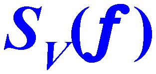
 v Svn ( f ) f Resulting output spectrum Sout ( f ) S sin ( f ) S sin ( f ) S out 3-17")
18 Output Spectrum with Phase Noise Suppose input noise to VCO (vn(t)) is bandlimited, non-periodic noise with spectrum Svn(f). In practice, derive phase spectrum as K S out ( f ) v Svn ( f ) f Resulting output spectrum Sout ( f ) S sin ( f ) S sin ( f ) S out 3-17 Ching-Yuan Yang / EE, NCHU
19 Measurement of Phase Noise in dbc/hz Sout(f) 1 S out(f) dbc/hz fo fo f Definition of L(f) Spectral density of noise L ( f ) 10 log Power of carrier Units are dbc/hz. For this case out ( f ) L ( f ) 10 log 10 log out ( f ) Valid when out(t) is small in deviation (i.e., when carrier is not modulated, as currently assumed) 3-18 Ching-Yuan Yang / EE, NCHU


 is set by ratio of noise density to carrier")
20 Single-Sided Version Definition of L(f) remains the same Spectral density of noise Power of carrier Units are dbc/hz. For this case So, we can work with either one-sided or two-sided spectral densities since L(f) is set by ratio of noise density to carrier power Ching-Yuan Yang / EE, NCHU
 Sout ( f ) S sin ( f ) S sin ( f ) S out 1 d spur f spur 1 d spur f spur 3-0 Ching-Yuan Yang / EE,")
21 Output Spectrum with Spurious Noise Suppose input noise to VCO is d vn (t ) spur cos( f spur t ) Kv out (t ) K v vn (t )dt Resulting output spectrum dspur f spur sin( f spur t ) Sout ( f ) S sin ( f ) S sin ( f ) S out 1 d spur f spur 1 d spur f spur 3-0 Ching-Yuan Yang / EE, NCHU
.")
22 Measurement of Spurious Noise in dbc 1 dspur f spur Definition of dbc Power of tone 10 log Power of carrier We are assuming double sided spectra, so integrate over positive and negative frequencies to get power. (Either single or double-sided spectra can be used in practice). For this case dspur dspur f spur 10 log dbc 0 log f spur 3-1 Ching-Yuan Yang / EE, NCHU


23 Phase noise in oscillators FkT 10 log P sig Measured in db below carrier per unit bandwidth. FkT Phase noise: L ( f ) 10 log Psig f1/ f 3 f f Q f Note: Leeson assumed that F( f) was constant over frequency. Hajimiri, IEEE JSSC, Mar Ching-Yuan Yang / EE, NCHU


 High frequencies")


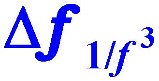
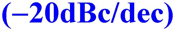
24 Phase Noise of A Practical Oscillator FkT 10 log Psig Phase noise drops at -0 db/decade over a wide frequency range, but deviates from this at: Low frequencies slope increases (often -30 db/decade) High frequencies slope flattens out (oscillator tank does not filter all noise sources) Frequency breakpoints and magnitude scaling are not readily predicted by the analysis approach taken so far. 3-3 Ching-Yuan Yang / EE, NCHU
 W o ( f ) E ( f ) The")
 W i ( f ) H ( f ) The untracked phase-noise")
 where W ( f ) W i ( f ) W o ( f ) and the subscript u indicates untracked phase noise.")
25 Phase-noise propagation in a PLL o, W o ( f ) i, W i ( f ) i e Ko s v o, W o ( f ) Phase-noise spectral density caused by the internal phase noise of VCO: Output phase-noise spectral density: W o o ( f ) W o ( f ) E ( f ) The phase error e due to o is o, so W e o ( f ) W o o ( f ) W o ( f ) E ( f ) (A) Phase-noise spectral density caused by input phase noise: The tracked phase-noise spectrum W o i ( f ) W i ( f ) H ( f ) The untracked phase-noise spectrum (phase-error spectrum) W e i ( f ) W i ( f ) E ( f ) Untracked jitter: (A) + (B) Wu ( f ) W ( f ) E ( f ) (B) where W ( f ) W i ( f ) W o ( f ) and the subscript u indicates untracked phase noise. 3-4 Ching-Yuan Yang / EE, NCHU
26 Bandwidth trade-off E( f ) has a highpass frequency response. An increase in PLL bandwidth K shifts the highpass corner to a higher frequency and reduces the integrated untracked phase jitter. This is opposite to the effect of bandwidth on phase jitter caused by additive noise. H( f ) has a lowpass frequency response. Total phase jitter cause by additive noise and phase noise: 0 '()()()() o n 0 W f H f df W f E f df 3-5 Ching-Yuan Yang / EE, NCHU
27 Delay-locked loops Vin Vout Vcont Voltage-Controlled Delay Line Vout Vin Phase Detector Charge Pump Low-Pass Filter Vc Delay line much less noisy than VCOs. First-order system (for first-order LPF), thus very stable. But input and output frequencies must be equal. 3-6 Ching-Yuan Yang / EE, NCHU
 (s) 1 E (s) e 1 H ( s) i ( s) 1 K d KVCDL F ( s ) Open-loop transfer function G ( s ) System transfer function Error transfer function 3-7 Ching-Yuan Yang / EE,")
28 Phase transfer function in linear model (DLL) i (s) Kd e (s) F (s) K VCDL o (s) o (s) K d KVCDL F ( s ) (loop gain) e (s) (s) K d KVCDL F ( s ) G (s) H (s) o i ( s ) 1 G ( s ) 1 K d KVCDL F ( s ) (s) 1 E (s) e 1 H ( s) i ( s) 1 K d KVCDL F ( s ) Open-loop transfer function G ( s ) System transfer function Error transfer function 3-7 Ching-Yuan Yang / EE, NCHU
29 3-8 Ching-Yuan Yang / EE, NCHU Transfer function of DLL Transfer function of PD/CP/LPF Close-loop transfer function Discussion The closed-loop transfer can be used to determine how out settles if in experiences a change. n, In practice R P may not be need because the loop contains only one pole at the origin.
30 Skew reduction Skew between data and buffered clock Use of a PLL to eliminate skew Use of a DLL to eliminate skew 3-9 Ching-Yuan Yang / EE, NCHU
Behavior of Phase-Locked Loops
 Phase-Locked Loops Behavior of Phase-Locked Loops Ching-Yuan Yang National Chung-Hsing University Department of Electrical Engineering Mathematical Model of VCOs 6- Phase of Signals V0 = Vmsin 0t V = Vmsin
LECTURE 3 CMOS PHASE LOCKED LOOPS
 Lecture 03 (8/9/18) Page 3-1 LECTURE 3 CMOS PHASE LOCKED LOOPS Topics The acquisition process unlocked state Noise in linear PLLs Organization: Systems Perspective Types of PLLs and PLL Measurements PLL
Introduction to Phase Locked Loop (PLL) DIGITAVID, Inc. Ahmed Abu-Hajar, Ph.D.
 DIGITAVID, Inc. Ahmed Abu-Hajar, Ph.D.") Introduction to Phase Locked Loop (PLL) DIGITAVID, Inc. Ahmed Abu-Hajar, Ph.D. abuhajar@digitavid.net Presentation Outline What is Phase Locked Loop (PLL) Basic PLL System Problem of Lock Acquisition Phase/Frequency
Introduction to Phase Locked Loop (PLL) DIGITAVID, Inc. Ahmed Abu-Hajar, Ph.D. abuhajar@digitavid.net Presentation Outline What is Phase Locked Loop (PLL) Basic PLL System Problem of Lock Acquisition Phase/Frequency
Voltage-Controlled Oscillator (VCO)
") Voltage-Controlled Oscillator (VCO) Desirable characteristics: Monotonic f osc vs. V C characteristic with adequate frequency range f max f osc Well-defined K vco f min slope = K vco VC V C in V K F(s)
Voltage-Controlled Oscillator (VCO) Desirable characteristics: Monotonic f osc vs. V C characteristic with adequate frequency range f max f osc Well-defined K vco f min slope = K vco VC V C in V K F(s)
Charge-Pump Phase-Locked Loops
 Phase-Locked Loos Charge-Pum Phase-Locked Loos Ching-Yuan Yang National Chung-Hsing University Deartment of Electrical Engineering Concetual oeration of a hase-frequency detector (PFD) PFD 5- Ching-Yuan
Tracking of Spread Spectrum Signals
 Chapter 7 Tracking of Spread Spectrum Signals 7. Introduction As discussed in the last chapter, there are two parts to the synchronization process. The first stage is often termed acquisition and typically
Design of CMOS Adaptive-Bandwidth PLL/DLLs
 Design of CMOS Adaptive-Bandwidth PLL/DLLs Jaeha Kim May 2004 At Samsung Electronics, Inc. Adaptive-Bandwidth PLL/DLL PLL/DLLs that scale their loop dynamics proportionally with the reference frequency
Introduction to CMOS RF Integrated Circuits Design
 V. Voltage Controlled Oscillators Fall 2012, Prof. JianJun Zhou V-1 Outline Phase Noise and Spurs Ring VCO LC VCO Frequency Tuning (Varactor, SCA) Phase Noise Estimation Quadrature Phase Generator Fall
Motivation for CDR: Deserializer (1)
") Motivation for CDR: Deserializer (1) Input data 1:2 DMUX 1:2 DMUX channel 1:2 DMUX Input clock 2 2 If input data were accompanied by a well-synchronized clock, deserialization could be done directly. EECS
Motivation for CDR: Deserializer (1) Input data 1:2 DMUX 1:2 DMUX channel 1:2 DMUX Input clock 2 2 If input data were accompanied by a well-synchronized clock, deserialization could be done directly. EECS
Switched-Capacitor Circuits David Johns and Ken Martin University of Toronto
 Switched-Capacitor Circuits David Johns and Ken Martin University of Toronto (johns@eecg.toronto.edu) (martin@eecg.toronto.edu) University of Toronto 1 of 60 Basic Building Blocks Opamps Ideal opamps usually
Lecture 120 Filters and Charge Pumps (6/9/03) Page 120-1
 Page 120-1") Lecture 120 Filters and Charge Pumps (6/9/03) Page 1201 LECTURE 120 FILTERS AND CHARGE PUMPS (READING: [4,6,9,10]) Objective The objective of this presentation is examine the circuits aspects of loop filters
Lecture 120 Filters and Charge Pumps (6/9/03) Page 1201 LECTURE 120 FILTERS AND CHARGE PUMPS (READING: [4,6,9,10]) Objective The objective of this presentation is examine the circuits aspects of loop filters
On Modern and Historical Short-Term Frequency Stability Metrics for Frequency Sources
 On Modern and Historical Short-Term Frequency Stability Metrics for Frequency Sources Michael S. McCorquodale, Ph.D. Founder and CTO, Mobius Microsystems, Inc. EFTF-IFCS, Besançon, France Session BL-D:
ELECTRONICS & COMMUNICATIONS DEP. 3rd YEAR, 2010/2011 CONTROL ENGINEERING SHEET 5 Lead-Lag Compensation Techniques
 CAIRO UNIVERSITY FACULTY OF ENGINEERING ELECTRONICS & COMMUNICATIONS DEP. 3rd YEAR, 00/0 CONTROL ENGINEERING SHEET 5 Lead-Lag Compensation Techniques [] For the following system, Design a compensator such
Lecture 310 Open-Loop Comparators (3/28/10) Page 310-1
 Page 310-1") Lecture 310 Open-Loop Comparators (3/28/10) Page 310-1 LECTURE 310 OPEN-LOOP COMPARATORS LECTURE ORGANIZATION Outline Characterization of comparators Dominant pole, open-loop comparators Two-pole, open-loop
Lecture 310 Open-Loop Comparators (3/28/10) Page 310-1 LECTURE 310 OPEN-LOOP COMPARATORS LECTURE ORGANIZATION Outline Characterization of comparators Dominant pole, open-loop comparators Two-pole, open-loop
2 nd Order PLL Design and Analysis
 nd Order PLL Design and Analysis S REF Phase Detector Σ K f Loop Filter VCO K V s R C Loop Divider Fig. : nd Order PLL with Current-Mode Phase Detector useful functions and identities Units Constants Table
Laboratory III: Operational Amplifiers
 Physics 33, Fall 2008 Lab III - Handout Laboratory III: Operational Amplifiers Introduction Operational amplifiers are one of the most useful building blocks of analog electronics. Ideally, an op amp would
Spurious-Tone Suppression Techniques Applied to a Wide-Bandwidth 2.4GHz Fractional-N PLL. University of California at San Diego, La Jolla, CA
 Spurious-Tone Suppression Techniques Applied to a Wide-Bandwidth 2.4GHz Fractional-N PLL Kevin Wang 1, Ashok Swaminathan 1,2, Ian Galton 1 1 University of California at San Diego, La Jolla, CA 2 NextWave
R a) Compare open loop and closed loop control systems. b) Clearly bring out, from basics, Force-current and Force-Voltage analogies.
 Compare open loop and closed loop control systems. b) Clearly bring out, from basics, Force-current and Force-Voltage analogies.") SET - 1 II B. Tech II Semester Supplementary Examinations Dec 01 1. a) Compare open loop and closed loop control systems. b) Clearly bring out, from basics, Force-current and Force-Voltage analogies..
SET - 1 II B. Tech II Semester Supplementary Examinations Dec 01 1. a) Compare open loop and closed loop control systems. b) Clearly bring out, from basics, Force-current and Force-Voltage analogies..
GATE EE Topic wise Questions SIGNALS & SYSTEMS
 www.gatehelp.com GATE EE Topic wise Questions YEAR 010 ONE MARK Question. 1 For the system /( s + 1), the approximate time taken for a step response to reach 98% of the final value is (A) 1 s (B) s (C)
Optoelectronic Applications. Injection Locked Oscillators. Injection Locked Oscillators. Q 2, ω 2. Q 1, ω 1
 Injection Locked Oscillators Injection Locked Oscillators Optoelectronic Applications Q, ω Q, ω E. Shumakher, J. Lasri,, B. Sheinman, G. Eisenstein, D. Ritter Electrical Engineering Dept. TECHNION Haifa
EE241 - Spring 2006 Advanced Digital Integrated Circuits
 EE241 - Spring 2006 Advanced Digital Integrated Circuits Lecture 20: Asynchronous & Synchronization Self-timed and Asynchronous Design Functions of clock in synchronous design 1) Acts as completion signal
Understanding Data Sheet Jitter Specifications for Cypress Timing Products
 for Cypress Timing Products Introduction This note describes how Cypress Semiconductor defines jitter for clock product specifications. There are several motivations for this. First, there is no accepted
Reciprocal Mixing: The trouble with oscillators
 Reciprocal Mixing: The trouble with oscillators Tradeoffs in RX Noise Figure(Sensitivity) Distortion (Linearity) Phase Noise (Aliasing) James Buckwalter Phase Noise Phase noise is the frequency domain
Oversampling Converters
 Oversampling Converters David Johns and Ken Martin (johns@eecg.toronto.edu) (martin@eecg.toronto.edu) slide 1 of 56 Motivation Popular approach for medium-to-low speed A/D and D/A applications requiring
Assessment.mcd. Comparison frequency at phase detector. Margin sought compared to ideal phase detector noise floor, db
 U029 PLL Synthesizer Phase Noise PLL Synthesizer Phase Noise FLO 9400 6 ω n 2π3000 Nominal loop natural frequency ζ 0.8 F ref 0 5 K v 2π500 6 0.005 K d 2π Nominal loop damping factor Comparison frequency
EECE 2150 Circuits and Signals Final Exam Fall 2016 Dec 16
 EECE 2150 Circuits and Signals Final Exam Fall 2016 Dec 16 Instructions: Write your name and section number on all pages Closed book, closed notes; Computers and cell phones are not allowed You can use
Short Course On Phase-Locked Loops and Their Applications Day 4, AM Lecture. Digital Frequency Synthesizers
 Short Course On Phase-Locked Loops and Their Applications Day 4, AM Lecture Digital Frequency Synthesizers Michael Perrott August 4, 2008 Copyright 2008 by Michael H. Perrott All rights reserved. Why Are
Principles of Communications Lecture 8: Baseband Communication Systems. Chih-Wei Liu 劉志尉 National Chiao Tung University
 Principles of Communications Lecture 8: Baseband Communication Systems Chih-Wei Liu 劉志尉 National Chiao Tung University cwliu@twins.ee.nctu.edu.tw Outlines Introduction Line codes Effects of filtering Pulse
Frequency Dependent Aspects of Op-amps
 Frequency Dependent Aspects of Op-amps Frequency dependent feedback circuits The arguments that lead to expressions describing the circuit gain of inverting and non-inverting amplifier circuits with resistive
Laplace Transform Analysis of Signals and Systems
 Laplace Transform Analysis of Signals and Systems Transfer Functions Transfer functions of CT systems can be found from analysis of Differential Equations Block Diagrams Circuit Diagrams 5/10/04 M. J.
INTRODUCTION TO DELTA-SIGMA ADCS
 ECE37 Advanced Analog Circuits INTRODUCTION TO DELTA-SIGMA ADCS Richard Schreier richard.schreier@analog.com NLCOTD: Level Translator VDD > VDD2, e.g. 3-V logic? -V logic VDD < VDD2, e.g. -V logic? 3-V
Lecture 4, Noise. Noise and distortion
 Lecture 4, Noise Noise and distortion What did we do last time? Operational amplifiers Circuit-level aspects Simulation aspects Some terminology Some practical concerns Limited current Limited bandwidth
Frequency Response. Re ve jφ e jωt ( ) where v is the amplitude and φ is the phase of the sinusoidal signal v(t). ve jφ
 where v is the amplitude and φ is the phase of the sinusoidal signal v(t). ve jφ") 27 Frequency Response Before starting, review phasor analysis, Bode plots... Key concept: small-signal models for amplifiers are linear and therefore, cosines and sines are solutions of the linear differential
27 Frequency Response Before starting, review phasor analysis, Bode plots... Key concept: small-signal models for amplifiers are linear and therefore, cosines and sines are solutions of the linear differential
Outline. Classical Control. Lecture 2
 Outline Outline Outline Review of Material from Lecture 2 New Stuff - Outline Review of Lecture System Performance Effect of Poles Review of Material from Lecture System Performance Effect of Poles 2 New
ECEN 610 Mixed-Signal Interfaces
 ECEN 610 Mixed-Signal Interfaces Sebastian Hoyos Texas A&M University Analog and Mixed Signal Group Spring 014 S. Hoyos-ECEN-610 1 Sample-and-Hold Spring 014 S. Hoyos-ECEN-610 ZOH vs. Track-and-Hold V(t)
On the Phase Noise and Noise Factor in Circuits and Systems - New Thoughts on an Old Subject
 On the Phase Noise and Noise Factor in Circuits and Systems - New Thoughts on an Old Subject Aleksandar Tasic QCT - Analog/RF Group Qualcomm Incorporated, San Diego A. Tasic 9 1 Outline Spectral Analysis
DATA receivers for digital transmission and storage systems
 IEEE TRANSACTIONS ON CIRCUITS AND SYSTEMS II: EXPRESS BRIEFS, VOL. 52, NO. 10, OCTOBER 2005 621 Effect of Loop Delay on Phase Margin of First-Order Second-Order Control Loops Jan W. M. Bergmans, Senior
CHAPTER 7 STEADY-STATE RESPONSE ANALYSES
 CHAPTER 7 STEADY-STATE RESPONSE ANALYSES 1. Introduction The steady state error is a measure of system accuracy. These errors arise from the nature of the inputs, system type and from nonlinearities of
Dynamic circuits: Frequency domain analysis
 Electronic Circuits 1 Dynamic circuits: Contents Free oscillation and natural frequency Transfer functions Frequency response Bode plots 1 System behaviour: overview 2 System behaviour : review solution
Time Response of Systems
 Chapter 0 Time Response of Systems 0. Some Standard Time Responses Let us try to get some impulse time responses just by inspection: Poles F (s) f(t) s-plane Time response p =0 s p =0,p 2 =0 s 2 t p =
ECE317 : Feedback and Control
 ECE317 : Feedback and Control Lecture : Steady-state error Dr. Richard Tymerski Dept. of Electrical and Computer Engineering Portland State University 1 Course roadmap Modeling Analysis Design Laplace
R. W. Erickson. Department of Electrical, Computer, and Energy Engineering University of Colorado, Boulder
 . W. Erickson Department of Electrical, Computer, and Energy Engineering University of Colorado, Boulder 8.1.7. The low-q approximation Given a second-order denominator polynomial, of the form G(s)= 1
Time Response Analysis (Part II)
") Time Response Analysis (Part II). A critically damped, continuous-time, second order system, when sampled, will have (in Z domain) (a) A simple pole (b) Double pole on real axis (c) Double pole on imaginary
Time Response Analysis (Part II). A critically damped, continuous-time, second order system, when sampled, will have (in Z domain) (a) A simple pole (b) Double pole on real axis (c) Double pole on imaginary
LECTURE 090 FILTERS AND CHARGE PUMPS
 Lecture 090 Filters and Charge Pumps (09/01/03) Page 0901 LECTURE 090 FILTERS AND CHARGE PUMPS Objective The objective of this presentation is to examine the circuits aspects of loop filters and charge
Linear Circuit Experiment (MAE171a) Prof: Raymond de Callafon
 Prof: Raymond de Callafon") Linear Circuit Experiment (MAE171a) Prof: Raymond de Callafon email: callafon@ucsd.edu TA: Younghee Han tel. (858) 8221763/8223457, email: y3han@ucsd.edu class information and lab handouts will be available
Linear Circuit Experiment (MAE171a) Prof: Raymond de Callafon email: callafon@ucsd.edu TA: Younghee Han tel. (858) 8221763/8223457, email: y3han@ucsd.edu class information and lab handouts will be available
WHITEPAPER: ACHIEVING THE CRAMER-RAO LOWER BOUND IN GPS TIME-OF-ARRIVAL ESTIMATION, A FREQUENCY DOMAIN WEIGHTED LEAST-SQUARES ESTIMATOR APPROACH
 WHITEPAPER: ACHIEVING THE CRAMER-RAO LOWER BOUND IN GPS TIME-OF-ARRIVAL ESTIMATION, A FREQUENCY DOMAIN WEIGHTED LEAST-SQUARES ESTIMATOR APPROACH KENNETH M PESYNA, JR AND TODD E HUMPHREYS THE UNIVERSITY
Lecture 6, ATIK. Switched-capacitor circuits 2 S/H, Some nonideal effects Continuous-time filters
 Lecture 6, ATIK Switched-capacitor circuits 2 S/H, Some nonideal effects Continuous-time filters What did we do last time? Switched capacitor circuits The basics Charge-redistribution analysis Nonidealties
Phase Noise in Oscillators
 Phase Noise in Oscillators V.Vasudevan, Department of Electrical Engineering, Indian Institute of Technology Madras Oscillator Spectrum Ideally, it should be one or more delta functions The actual spectrum
Linear Phase-Noise Model
 Linear Phase-Noise Model 41 Sub-Outline Generic Linear Phase-Noise Model Circuit-Specific Linear Phase-Noise Model 4 Generic Linear Phase-Noise Model - Outline Linear Oscillator Model LC-Tank noise active
Review of Linear Time-Invariant Network Analysis
 D1 APPENDIX D Review of Linear Time-Invariant Network Analysis Consider a network with input x(t) and output y(t) as shown in Figure D-1. If an input x 1 (t) produces an output y 1 (t), and an input x
Optimization of Phase-Locked Loops With Guaranteed Stability. C. M. Kwan, H. Xu, C. Lin, and L. Haynes
 Optimization of Phase-Locked Loops With Guaranteed Stability C. M. Kwan, H. Xu, C. Lin, and L. Haynes ntelligent Automation nc. 2 Research Place Suite 202 Rockville, MD 20850 phone: (301) - 590-3155, fax:
Chapter 4 Code Tracking Loops
 Chapter 4 Code Tracking Loops 4- Optimum Tracking of Wideband Signals A tracking loop making use of this optimum discriminator is illustrated in Figure 4-1. 4- Optimum Tracking of Wideband Signals 4.3
Signals and Spectra - Review
 Signals and Spectra - Review SIGNALS DETERMINISTIC No uncertainty w.r.t. the value of a signal at any time Modeled by mathematical epressions RANDOM some degree of uncertainty before the signal occurs
24.2: Self-Biased, High-Bandwidth, Low-Jitter 1-to-4096 Multiplier Clock Generator PLL
 24.2: Self-Biased, High-Bandwidth, Low-Jitter 1-to-4096 Multiplier Clock Generator PLL John G. Maneatis 1, Jaeha Kim 1, Iain McClatchie 1, Jay Maxey 2, Manjusha Shankaradas 2 True Circuits, Los Altos,
Notes on DPLL. Haiyun Tang Most of material is derived from Chistian s report[4]
![Notes on DPLL. Haiyun Tang Most of material is derived from Chistian s report[4]](/thumbs/92/108041545.jpg "Notes on DPLL. Haiyun Tang Most of material is derived from Chistian s report[4]") Notes on DPLL Haiyun Tang tangh@eecs.berkeley.edu Most of material is derived from Chistian s report[4] 1 Input Signal x(t) Phase Detector Error Signal e(t) Loop Filter L(s) Control Signal c(t) VCO Output
Notes on DPLL Haiyun Tang tangh@eecs.berkeley.edu Most of material is derived from Chistian s report[4] 1 Input Signal x(t) Phase Detector Error Signal e(t) Loop Filter L(s) Control Signal c(t) VCO Output
ECE Branch GATE Paper The order of the differential equation + + = is (A) 1 (B) 2
 1 (B) 2") Question 1 Question 20 carry one mark each. 1. The order of the differential equation + + = is (A) 1 (B) 2 (C) 3 (D) 4 2. The Fourier series of a real periodic function has only P. Cosine terms if it is
Question 1 Question 20 carry one mark each. 1. The order of the differential equation + + = is (A) 1 (B) 2 (C) 3 (D) 4 2. The Fourier series of a real periodic function has only P. Cosine terms if it is
Outline. Introduction Delay-Locked Loops. DLL Applications Phase-Locked Loops PLL Applications
 Introduction Delay-Locked Loops DLL overview CMOS, refreshg your memory Buildg blocks: VCDL PD LF DLL analysis: Lear Nonlear Lock acquisition Charge sharg DLL Applications Phase-Locked Loops PLL Applications
Frequency Detection of CDRs (1)
") Frequency Detection of CDs (1) ecall that faster PLL locking can be accomplished by use of a phase-frequency detector (PFD): V in V up V up V dn -4 π -2 π +2 π +4 π φ in φ out 2V swing V f V dn K pd =
Frequency Detection of CDs (1) ecall that faster PLL locking can be accomplished by use of a phase-frequency detector (PFD): V in V up V up V dn -4 π -2 π +2 π +4 π φ in φ out 2V swing V f V dn K pd =
DUE to its practical importance in communications, the
 IEEE TRANSACTIONS ON CIRCUITS AND SYSTEMS II: EXPRESS BRIEFS, VOL. 52, NO. 3, MARCH 2005 149 An Analytical Formulation of Phase Noise of Signals With Gaussian-Distributed Jitter Reza Navid, Student Member,
Exercises for lectures 13 Design using frequency methods
 Exercises for lectures 13 Design using frequency methods Michael Šebek Automatic control 2016 31-3-17 Setting of the closed loop bandwidth At the transition frequency in the open loop is (from definition)
System on a Chip. Prof. Dr. Michael Kraft
 System on a Chip Prof. Dr. Michael Kraft Lecture 3: Sample and Hold Circuits Switched Capacitor Circuits Circuits and Systems Sampling Signal Processing Sample and Hold Analogue Circuits Switched Capacitor
Fundamentals: Frequency & Time Generation
 Fundamentals: Frequency & Time Generation Dominik Schneuwly Oscilloquartz SA slide 1 v.1.0 24/10/12 SCDO Content 1. Fundamentals 2. Frequency Generation Atomic Cesium Clock (Cs) Rubidium Oscillator (Rb)
Chapter 9: Controller design
 Chapter 9. Controller Design 9.1. Introduction 9.2. Effect of negative feedback on the network transfer functions 9.2.1. Feedback reduces the transfer function from disturbances to the output 9.2.2. Feedback
Solutions to Problems in Chapter 4
 Solutions to Problems in Chapter 4 Problems with Solutions Problem 4. Fourier Series of the Output Voltage of an Ideal Full-Wave Diode Bridge Rectifier he nonlinear circuit in Figure 4. is a full-wave
Quantization Noise Conditioning Techniques for Digital Delta-Sigma Modulators
 Proceedings of the 19th International Symposium on Mathematical Theory of Networks and Systems MTNS 2010 5 9 July, 2010 Budapest, Hungary Quantization Noise Conditioning Techniques for Digital Delta-Sigma
Charge Pump. Loop Filter. VCO Divider
 FEATURES PIN CONFIGURATION Low phase noise XO Input from crystal or clock at 10-27MHz. Integrated crystal load capacitor: no external load capacitor required. Output clocks up to 160MHz. Low phase noise
Dallas Semiconductor 17
 2 3 8 11 Dallas Semiconductor 17 15 KEITHLEY MODEL 2304 6.0V, 750mA (SOURCE) A B KEITHLEY MODEL 2304 (LOAD) 150Ω 100Ω 4.7kΩ 1kΩ CC V IN 1400mAh Li-POLYMER CELL PC 100Ω DQ V DD 5.1V 0.1µF SNS V SS 0.1µF
Digital Band-pass Modulation PROF. MICHAEL TSAI 2011/11/10
 Digital Band-pass Modulation PROF. MICHAEL TSAI 211/11/1 Band-pass Signal Representation a t g t General form: 2πf c t + φ t g t = a t cos 2πf c t + φ t Envelope Phase Envelope is always non-negative,
SYLLABUS. osmania university CHAPTER - 1 : TRANSIENT RESPONSE CHAPTER - 2 : LAPLACE TRANSFORM OF SIGNALS
 i SYLLABUS osmania university UNIT - I CHAPTER - 1 : TRANSIENT RESPONSE Initial Conditions in Zero-Input Response of RC, RL and RLC Networks, Definitions of Unit Impulse, Unit Step and Ramp Functions,
HIGH-PERFORMANCE phase-locked loops (PLLs) are
 are") IEEE TRANSACTIONS ON CIRCUITS AND SYSTEMS I: REGULAR PAPERS 1 Multi-Rate DEM With Mismatch-Noise Cancellation for DCOs in Digital PLLs Enrique Alvarez-Fontecilla, Christian Venerus, Member, IEEE, and Ian
IEEE TRANSACTIONS ON CIRCUITS AND SYSTEMS I: REGULAR PAPERS 1 Multi-Rate DEM With Mismatch-Noise Cancellation for DCOs in Digital PLLs Enrique Alvarez-Fontecilla, Christian Venerus, Member, IEEE, and Ian
Principles of Communications
 Principles of Communications Weiyao Lin, PhD Shanghai Jiao Tong University Chapter 4: Analog-to-Digital Conversion Textbook: 7.1 7.4 2010/2011 Meixia Tao @ SJTU 1 Outline Analog signal Sampling Quantization
L L, R, C. Kirchhoff s rules applied to AC circuits. C Examples: Resonant circuits: series and parallel LRC. Filters: narrowband,
 Today in Physics 1: A circuits Solving circuit problems one frequency at a time. omplex impedance of,,. Kirchhoff s rules applied to A circuits. it V in Examples: esonant circuits: i series and parallel.
Quartz Crystal Oscillators and Phase Locked Loops. Dominik Schneuwly Yves Schwab
 Quartz Crystal Oscillators and Phase Locked Loops Dominik Schneuwly Yves Schwab Ed. 2006-02 D. Schneuwly Slide 1 Content 1. Quartz Crystal Resonator Technology Quartz, crystal lattice and piezo-electric
KINGS COLLEGE OF ENGINEERING DEPARTMENT OF ELECTRONICS AND COMMUNICATION ENGINEERING
 KINGS COLLEGE OF ENGINEERING DEPARTMENT OF ELECTRONICS AND COMMUNICATION ENGINEERING QUESTION BANK SUB.NAME : CONTROL SYSTEMS BRANCH : ECE YEAR : II SEMESTER: IV 1. What is control system? 2. Define open
Second and Higher-Order Delta-Sigma Modulators
 Second and Higher-Order Delta-Sigma Modulators MEAD March 28 Richard Schreier Richard.Schreier@analog.com ANALOG DEVICES Overview MOD2: The 2 nd -Order Modulator MOD2 from MOD NTF (predicted & actual)
Chapter 12 Variable Phase Interpolation
 Chapter 12 Variable Phase Interpolation Contents Slide 1 Reason for Variable Phase Interpolation Slide 2 Another Need for Interpolation Slide 3 Ideal Impulse Sampling Slide 4 The Sampling Theorem Slide
EECE 2150 Circuits and Signals Final Exam Fall 2016 Dec 12
 EECE 2150 Circuits and Signals Final Exam Fall 2016 Dec 12 Instructions: Write your name and section number on all pages Closed book, closed notes; Computers and cell phones are not allowed You can use
A New Approach for Computation of Timing Jitter in Phase Locked Loops
 A New Approach for Computation of Timing Jitter in Phase ocked oops M M. Gourary (1), S. G. Rusakov (1), S.. Ulyanov (1), M.M. Zharov (1),.. Gullapalli (2), and B. J. Mulvaney (2) (1) IPPM, Russian Academy
University of Toronto Faculty of Applied Science and Engineering. ECE212H1F - Circuit Analysis. Final Examination December 16, :30am - noon
 , LAST name: First name: Student ID: University of Toronto Faculty of Applied Science and Engineering ECE212H1F - Circuit Analysis Final Examination December 16, 2017 9:30am - noon Guidelines: Exam type:
Homework Assignment No. 3 - Solutions
 ECE 6440 Summer 2003 Page 1 Homework Aignment o. 3 Problem 1 (10 point) Aume an LPLL ha F() 1 and the PLL parameter are 0.8V/radian, K o 100 MHz/V, and the ocillation frequency, f oc 500MHz. Sketch the
Appendix A: Exercise Problems on Classical Feedback Control Theory (Chaps. 1 and 2)
") Appendix A: Exercise Problems on Classical Feedback Control Theory (Chaps. 1 and 2) For all calculations in this book, you can use the MathCad software or any other mathematical software that you are familiar
Appendix A: Exercise Problems on Classical Feedback Control Theory (Chaps. 1 and 2) For all calculations in this book, you can use the MathCad software or any other mathematical software that you are familiar
Oscillator Phase Noise
 Berkeley Oscillator Phase Noise Prof. Ali M. U.C. Berkeley Copyright c 2014 by Ali M. Oscillator Output Spectrum Ideal Oscillator Spectrum Real Oscillator Spectrum The output spectrum of an oscillator
( s) N( s) ( ) The transfer function will take the form. = s = 2. giving ωo = sqrt(1/lc) = 1E7 [rad/s] ω 01 := R 1. α 1 2 L 1.
![( s) N( s) ( ) The transfer function will take the form. = s = 2. giving ωo = sqrt(1/lc) = 1E7 [rad/s] ω 01 := R 1. α 1 2 L 1.](/thumbs/83/87520964.jpg "( s) N( s) ( ) The transfer function will take the form. = s = 2. giving ωo = sqrt(1/lc) = 1E7 [rad/s] ω 01 := R 1. α 1 2 L 1.") Problem ) RLC Parallel Circuit R L C E-4 E-0 V a. What is the resonant frequency of the circuit? The transfer function will take the form N ( ) ( s) N( s) H s R s + α s + ω s + s + o L LC giving ωo sqrt(/lc)
Problem ) RLC Parallel Circuit R L C E-4 E-0 V a. What is the resonant frequency of the circuit? The transfer function will take the form N ( ) ( s) N( s) H s R s + α s + ω s + s + o L LC giving ωo sqrt(/lc)
High-Speed Serial Interface Circuits and Systems. Lect. 4 Phase-Locked Loop (PLL) Type 1 (Chap. 8 in Razavi)
 Type 1 (Chap. 8 in Razavi)") High-Speed Serial Iterface Circuit ad Sytem Lect. 4 Phae-Locked Loop (PLL) Type 1 (Chap. 8 i Razavi) PLL Phae lockig loop A (egative-feedback) cotrol ytem that geerate a output igal whoe phae (ad frequecy)
High-Speed Serial Iterface Circuit ad Sytem Lect. 4 Phae-Locked Loop (PLL) Type 1 (Chap. 8 i Razavi) PLL Phae lockig loop A (egative-feedback) cotrol ytem that geerate a output igal whoe phae (ad frequecy)
Discrete Time Signals and Switched Capacitor Circuits (rest of chapter , 10.2)
") Discrete Time Signals and Switched Capacitor Circuits (rest of chapter 9 + 0., 0.2) Tuesday 6th of February, 200, 9:5 :45 Snorre Aunet, sa@ifi.uio.no Nanoelectronics Group, Dept. of Informatics Office
Discrete Time Signals and Switched Capacitor Circuits (rest of chapter 9 + 0., 0.2) Tuesday 6th of February, 200, 9:5 :45 Snorre Aunet, sa@ifi.uio.no Nanoelectronics Group, Dept. of Informatics Office
Table of Laplacetransform
 Appendix Table of Laplacetransform pairs 1(t) f(s) oct), unit impulse at t = 0 a, a constant or step of magnitude a at t = 0 a s t, a ramp function e- at, an exponential function s + a sin wt, a sine fun
MAS107 Control Theory Exam Solutions 2008
 MAS07 CONTROL THEORY. HOVLAND: EXAM SOLUTION 2008 MAS07 Control Theory Exam Solutions 2008 Geir Hovland, Mechatronics Group, Grimstad, Norway June 30, 2008 C. Repeat question B, but plot the phase curve
ECEN620: Network Theory Broadband Circuit Design Fall 2018
 ECEN60: Network Theory Broadband Circuit Deign Fall 08 Lecture 6: Loop Filter Circuit Sam Palermo Analog & Mixed-Signal Center Texa A&M Univerity Announcement HW i due Oct Require tranitor-level deign
SNR Calculation and Spectral Estimation [S&T Appendix A]
![SNR Calculation and Spectral Estimation [S&T Appendix A]](/thumbs/75/71929358.jpg "SNR Calculation and Spectral Estimation [S&T Appendix A]") SR Calculation and Spectral Estimation [S&T Appendix A] or, How not to make a mess of an FFT Make sure the input is located in an FFT bin 1 Window the data! A Hann window works well. Compute the FFT 3
SR Calculation and Spectral Estimation [S&T Appendix A] or, How not to make a mess of an FFT Make sure the input is located in an FFT bin 1 Window the data! A Hann window works well. Compute the FFT 3
C(s) R(s) 1 C(s) C(s) C(s) = s - T. Ts + 1 = 1 s - 1. s + (1 T) Taking the inverse Laplace transform of Equation (5 2), we obtain
 R(s) 1 C(s) C(s) C(s) = s - T. Ts + 1 = 1 s - 1. s + (1 T) Taking the inverse Laplace transform of Equation (5 2), we obtain") analyses of the step response, ramp response, and impulse response of the second-order systems are presented. Section 5 4 discusses the transient-response analysis of higherorder systems. Section 5 5 gives
analyses of the step response, ramp response, and impulse response of the second-order systems are presented. Section 5 4 discusses the transient-response analysis of higherorder systems. Section 5 5 gives
EC CONTROL SYSTEM UNIT I- CONTROL SYSTEM MODELING
 EC 2255 - CONTROL SYSTEM UNIT I- CONTROL SYSTEM MODELING 1. What is meant by a system? It is an arrangement of physical components related in such a manner as to form an entire unit. 2. List the two types
Performance of Feedback Control Systems
 Performance of Feedback Control Systems Design of a PID Controller Transient Response of a Closed Loop System Damping Coefficient, Natural frequency, Settling time and Steady-state Error and Type 0, Type
INTRODUCTION TO DELTA-SIGMA ADCS
 ECE1371 Advanced Analog Circuits Lecture 1 INTRODUCTION TO DELTA-SIGMA ADCS Richard Schreier richard.schreier@analog.com Trevor Caldwell trevor.caldwell@utoronto.ca Course Goals Deepen understanding of
(b) A unity feedback system is characterized by the transfer function. Design a suitable compensator to meet the following specifications:
 A unity feedback system is characterized by the transfer function. Design a suitable compensator to meet the following specifications:") 1. (a) The open loop transfer function of a unity feedback control system is given by G(S) = K/S(1+0.1S)(1+S) (i) Determine the value of K so that the resonance peak M r of the system is equal to 1.4.
1. (a) The open loop transfer function of a unity feedback control system is given by G(S) = K/S(1+0.1S)(1+S) (i) Determine the value of K so that the resonance peak M r of the system is equal to 1.4.
MODULE I. Transient Response:
 Transient Response: MODULE I The Transient Response (also known as the Natural Response) is the way the circuit responds to energies stored in storage elements, such as capacitors and inductors. If a capacitor
Time-Varying, Frequency-Domain Modeling and Analysis of Phase-Locked Loops with Sampling Phase-Frequency Detectors
 Time-Varying, Frequency-Domain Modeling and Analysis of Phase-Locked Loops with Sampling Phase-Frequency Detectors Piet Vanassche, Georges Gielen and Willy Sansen Katholieke Universiteit Leuven - ESAT/MICAS
Process Control & Instrumentation (CH 3040)
") First-order systems Process Control & Instrumentation (CH 3040) Arun K. Tangirala Department of Chemical Engineering, IIT Madras January - April 010 Lectures: Mon, Tue, Wed, Fri Extra class: Thu A first-order
First-order systems Process Control & Instrumentation (CH 3040) Arun K. Tangirala Department of Chemical Engineering, IIT Madras January - April 010 Lectures: Mon, Tue, Wed, Fri Extra class: Thu A first-order
Review of 1 st Order Circuit Analysis
 ECEN 60 Circuits/Electronics Spring 007-7-07 P. Mathys Review of st Order Circuit Analysis First Order Differential Equation Consider the following circuit with input voltage v S (t) and output voltage
Discrete Time Signals and Switched Capacitor Circuits (rest of chapter , 10.2)
") Discrete Time Signals and Switched Capacitor Circuits (rest of chapter 9 + 10.1, 10.2) Tuesday 16th of February, 2010, 0, 9:15 11:45 Snorre Aunet, sa@ifi.uio.no Nanoelectronics Group, Dept. of Informatics
Discrete Time Signals and Switched Capacitor Circuits (rest of chapter 9 + 10.1, 10.2) Tuesday 16th of February, 2010, 0, 9:15 11:45 Snorre Aunet, sa@ifi.uio.no Nanoelectronics Group, Dept. of Informatics
EE C128 / ME C134 Fall 2014 HW 8 - Solutions. HW 8 - Solutions
 EE C28 / ME C34 Fall 24 HW 8 - Solutions HW 8 - Solutions. Transient Response Design via Gain Adjustment For a transfer function G(s) = in negative feedback, find the gain to yield a 5% s(s+2)(s+85) overshoot