Lecture 4, Noise. Noise and distortion
|
|
|
- Hillary Garrett
- 5 years ago
- Views:
Transcription

1 Lecture 4, Noise Noise and distortion
2 What did we do last time? Operational amplifiers Circuit-level aspects Simulation aspects Some terminology Some practical concerns Limited current Limited bandwidth etc 113 of 34
3 What will we do today? Noise Circuit noise Thermal noise Flicker noise Distortion What sets the (non)linearity in our CMOS devices? 114 of 34

4 The "741 amplifier" Texas instruments opa what is the bandwidth? opa what is the DC gain? Analog Devices AD854x - what is the DC gain, or what is the open-loop bandwidth? 115 of 34
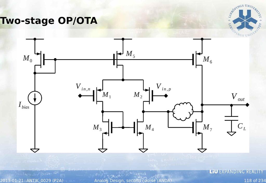
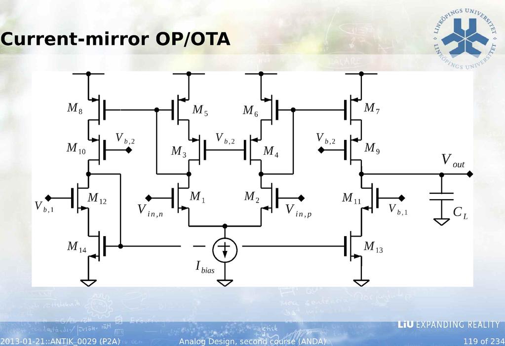
5 Operational amplifier architectures Left-overs Examples Telescopic Two-stage Folded-cascode Current-mirror Essentially just cascaded stages of different kinds 116 of 34
6 Telescopic OTA Stack many cascodes on top of each-other and use gainboosting, etc. Omitted, since it is not applicable for modern processes. The swing is eaten up. 117 of 34
7
8
9 Folded-cascode OP/OTA V b,1 V b, V out, p V b,3 CL V b,4 M3 M4 M6 M9 M 11 M7 V i n,n M1 M V in,p V b,5 M5 M8 M 10 V b, V out, n V b,3 CL V b,4 10 of 34
10 OP/OTA Compilation Cookbook recipes Hand-outs with step-by-step explanation of the design of OP/OTAs NN_LN_opampHandsouts_A.pdf Compensation techniques NN_LN_opampCompensationTable_A.pdf 11 of 34
11 Amplifier classes Not really covered in this course. Different classes, such as Class A, B, AB, C, D, E, F, G, H, I, K, S, T, Z, etc. Class A Essentially the common-source stage Class AB Essentially a push-pull configured class A 1 of 34
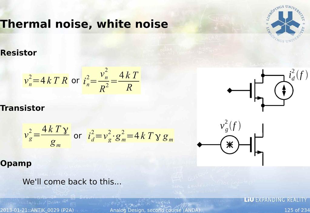
12 Noise Any circuit has noise and you, as a designer, have to reduce it or minimize the impact of it "A disturbance, especially a random and persistent disturbance, that obscures or reduces the clarity of a signal." Consequences We need to use stochastic variables and power spectral densities, expectation values, etc. We need to make certain assumptions (models) of our noise sources in order to calculate 13 of 34

13 Superfunction and spectral densitites Power spectral density (PSD) Superfunction S 0 f = Ai f S i f Total noise V tot = v n f df Brickwall noise p1 V =v 0 4 tot n 14 of 34
14
15 Flicker noise, 1/f-noise, pink noise Resistor bias v k and i = R v n v= n W L f n Transistor S f 1 C ox W L f KF 1 v = and i d = g m v n C ox W L f g KF 4kT gm log f 16 of 34
16
17
18
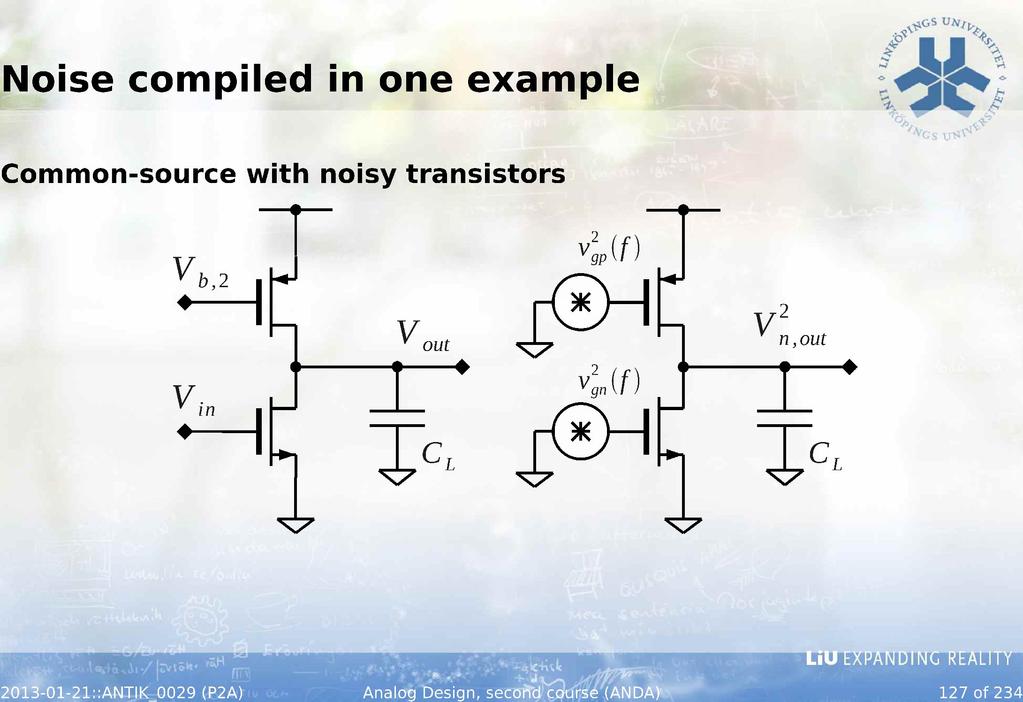
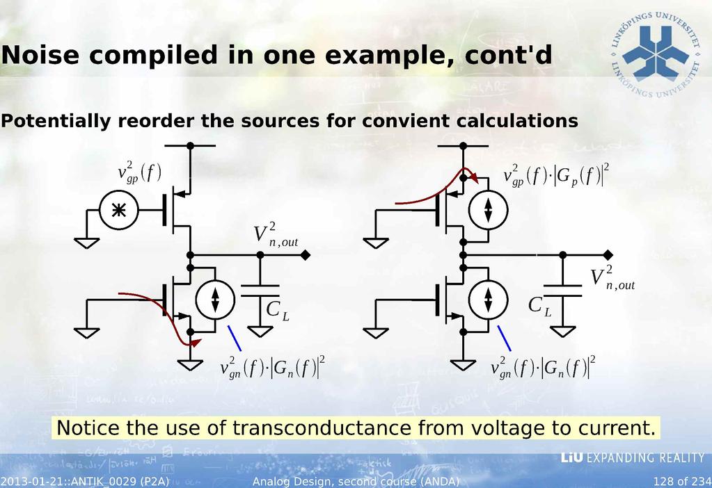
19 Noise compiled in one example, cont'd The general transfer function to the output is given by V n, out f = gn gp v f G n f v f G p f s C L g p g n Insert the values mn V n, out f =4 k T mp g g g mn g mp s g p g n g p g n 1 CL g mn g mp =4 k T g p g n s g p g n 1 CL 130 of 34
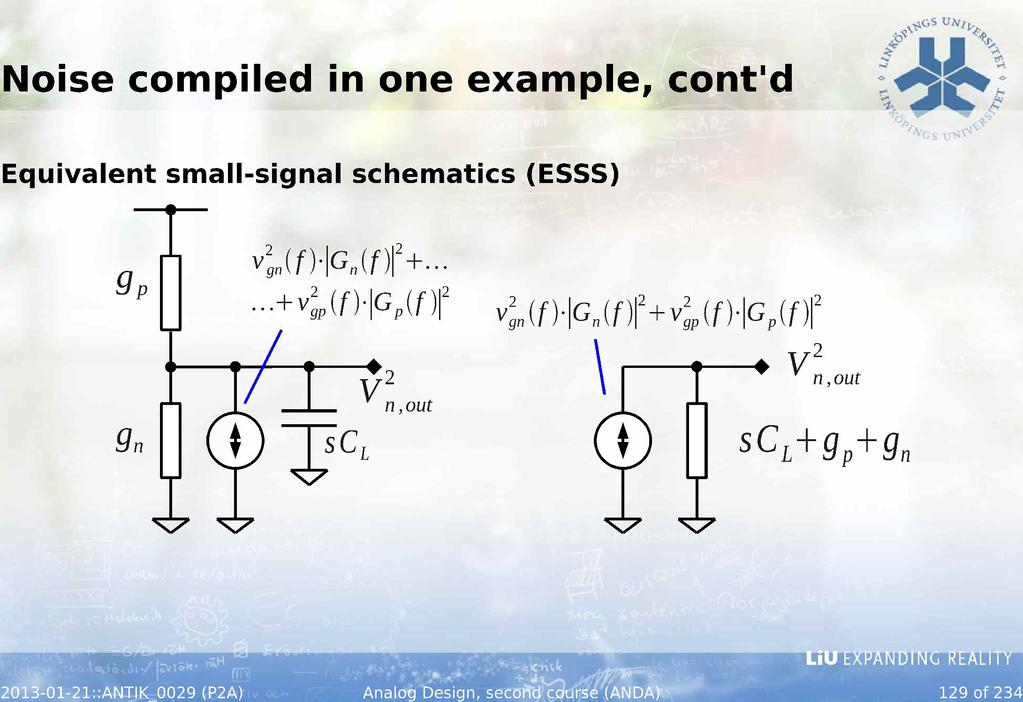
20 Noise compiled in one example, cont'd Use the brickwall approach p1 V = V f =V 0 4 g mn g mp g p g n k T g mn g mp V n, tot =4 k T = CL g p g n g p g n 4C L n, tot n, out n, out Conclude V n, tot g mp kt = A0 1 CL g mn kt/c noise! 131 of 34
21
22 The common-source example Input-referred noise V n,i n [ f = 4 k T g mn g mp g p g n s 1 g p g n CL [ ] ] s 1 g p g n CL g mn g p g n g mp 4kT = 1 g mn g mn 133 of 34
23 What does this mean? Bias transistor should be made with low transconductance! Visible from the formula Gain transistors should be made with high transconductance! Visible from the formula Gain should be distributed between multiple stages (Friis) Left as an exercise 134 of 34
24
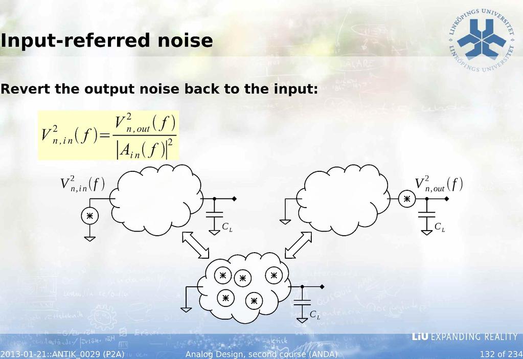
25 Example from "741" opamp OPA336N (Texas Instruments) Input Voltage Noise, f = 0.1 to 10 Hz Input Voltage Noise Density, f = 1 khz Current Noise Density, f = 1 khz 3 μvp-p (e n ) (i n ) 40 nv/ Hz 30 fa/ Hz 136 of 34
26 Example from "741" opamp 137 of 34
27
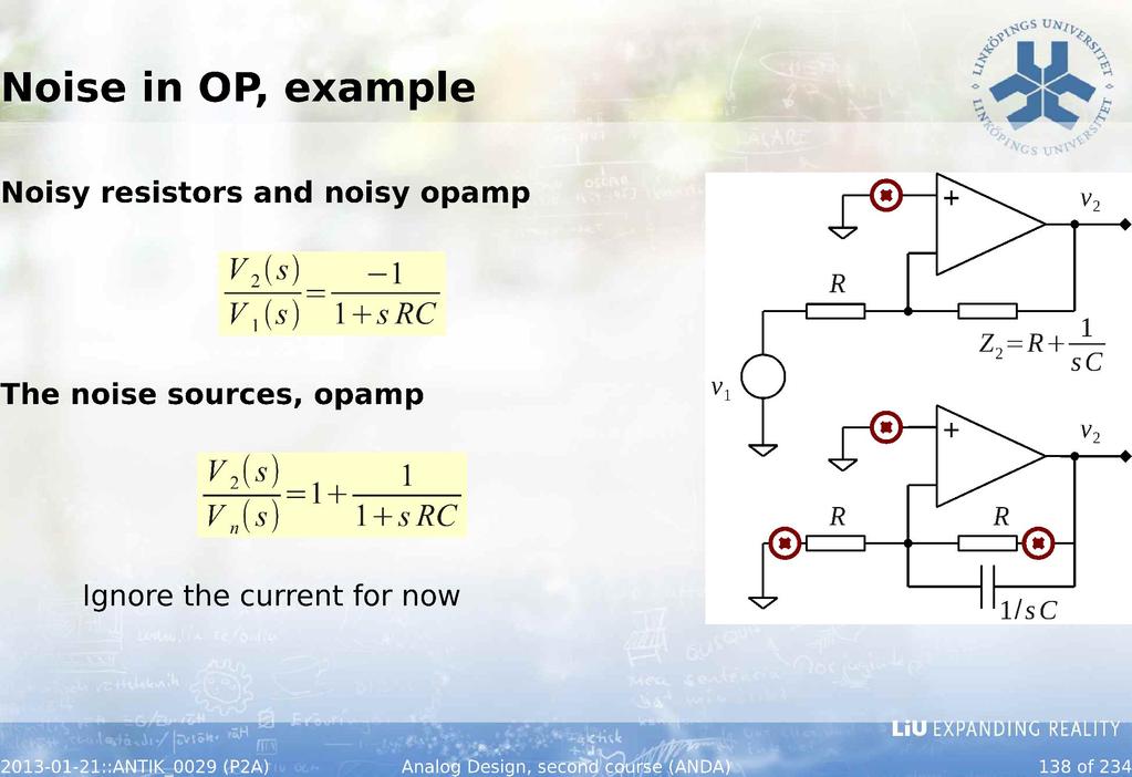
28 Noise in OP, example cont'd PSD 1 S n ( f )= j π f RC A nasty transfer function - the noise never reaches zero! Practically The opamp unity-gain bandwidth will bandlimit the noise for which we can use the brickwall approach: P tot, op v n, op ωug (0) of 34
29 Noise in OP, example cont'd The noise sources, resistors V s V s 1 1 = = and V r s 1 s RC V r1 s 1 s RC PSD 1 S n ( f )= 1+ j π f RC A low-pass filter response - use the brickwall approach 1/ RC P tot, R v n, R (0) of 34
30 Noise in OP, example cont'd Combined P tot =P tot, R+P tot, op v P tot v n, op n, op ωug 1/ RC (0) + v n, R (0) 4 4 ωug ωug k T 1/ RC (0) +4 k T R =v n, op (0) + C This is the power normalized over 1 Ohm We could define the rms voltage as: v o, rms= P tot v n, op ωug k T (0) + C 141 of 34
31 Noise in OP, example cont'd, values Example: C =1 nf, R=10 kohm, i.e., a bandwidth of f bw 14 -khz OPA336: v n, op (0) sqv/hz, and f ug 100 khz P tot = or v o, rms 9.4 uv (compare with the reported 3 uv in the data sheet) 14 of 34
32 Signal-to-noise ratio (SNR) At the output of our system, we will have a certain signal power. The signal-to-noise ratio (SNR) determines the quality of the system: P sig v s, rms P sig or SNR=10 log 10 or SNR=0 log 10 SNR= P noise v n, rms P noise ( ) ( ) OPA336 example Assume signal swing at output is v rms =1 V. Then the SNR is SNR 0 log10 ( db (approximately 16 bits) ) 143 of 34
33 Distortion Frequency-domain measures Spurious-free dynamic range, SFDR Harmonic distortion, HD Signal-to-noise-and-distortion ratio, SNDR Amplitude domain measures Compression (clipping) Offset 144 of 34
34 Distortion No circuit is fully linear Y = 0 1 X X 3 X 4 X Example X =sin t is the sinusoidal, steady-state signal 1=1, =0.01 are the characteristic coefficients of the system Results in an output as 1 cos ω t Y (t )=sin ω t +α sin ω t =sin ω t +α 145 of 34
35 Distortion, cont'd Results in a DC shift and a distortion term Y= sin t cos t desired DC shift distortion Harmonic distortion 1 1 HD = = =40000, ( α / ) (0.01/ ) i.e., approximately 46 db 146 of 34
36 Frequency domain measures 147 of 34
37 Distortion, fully differential circuits Assume distortion is identical in two branches 3 4 Y p= 0 1 X p X p 3 X p 4 X p 3 and 4 Y n= 0 1 X n X n 3 X n 4 X n Difference Y =Y p Y n= X p X n X p X n Further on, assume input is already OK X p = X n= X 148 of 34
38 Distortion, fully differential, cont'd Results in Y = 1 X p X p X p X p 3 X 3p X p 3 and eventually 3 Y = 1 X X 3 4 Even-order terms disappear! 149 of 34
39 Distortion in a common-source Assume a common-source stage with resistive load First-order model I D = V eff RL V out =V DD R I D =V DD R V eff V out Assume a limited input signal (no clipping) V in V eff t =V eff0 V x sin t Form the output V out t =V DD R V eff0 V x sin t V out (t )=V DD R α ( V eff0 +V eff0 V x sin ω t+v x sin ωt ) 150 of 34
40 Distortion in a common-source, cont'd Continue to rewrite using trigonometrics V x V out (t )=V DD R α V eff0 + V eff0 V x sin ω t + (1 cos ω t ) ( ) Analyze V V x V out (t )=V DD R α V eff0 + x + V V R α sin ω t cos ω t eff0 x DC desired signal distortion 151 of 34
41 Compression analysis Signal power scales "linearly" with amplitude V V x V out (t )=V DD R α V eff0 + x + V V R α sin ω t cos ω t eff0 x desired signal DC distortion Distortion power scales "quadratically" At some point they will meet. Intercept points Output and input-referred IIP, OIP Common measures of nonlinearity 15 of 34
42 Distortion vs Noise, concludingly High signal power gives high signal-to-noise ratio High signal power gives low signal-to-distortion ratio This means that you need to distribute the gain between the different stages accordingly and trade-off between the two. 153 of 34
43 What did we do today? Noise Circuit noise Thermal noise Flicker noise Distortion What sets the (non)linearity in our CMOS devices? 154 of 34
44 What will we do next time? PCB vs silicon What are the differences when scaling up the geometries Components Surface-mounted components PCB Some PCB specifics 155 of 34
Lecture 6, ATIK. Switched-capacitor circuits 2 S/H, Some nonideal effects Continuous-time filters
 Lecture 6, ATIK Switched-capacitor circuits 2 S/H, Some nonideal effects Continuous-time filters What did we do last time? Switched capacitor circuits The basics Charge-redistribution analysis Nonidealties
Guest Lectures for Dr. MacFarlane s EE3350
 Guest Lectures for Dr. MacFarlane s EE3350 Michael Plante Sat., -08-008 Write name in corner.. Problem Statement Amplifier Z S Z O V S Z I Z L Transducer, Antenna, etc. Coarse Tuning (optional) Amplifier
Lecture 7, ATIK. Continuous-time filters 2 Discrete-time filters
 Lecture 7, ATIK Continuous-time filters 2 Discrete-time filters What did we do last time? Switched capacitor circuits with nonideal effects in mind What should we look out for? What is the impact on system
Advanced Current Mirrors and Opamps
 Advanced Current Mirrors and Opamps David Johns and Ken Martin (johns@eecg.toronto.edu) (martin@eecg.toronto.edu) slide 1 of 26 Wide-Swing Current Mirrors I bias I V I in out out = I in V W L bias ------------
3. Basic building blocks. Analog Design for CMOS VLSI Systems Franco Maloberti
 Inverter with active load It is the simplest gain stage. The dc gain is given by the slope of the transfer characteristics. Small signal analysis C = C gs + C gs,ov C 2 = C gd + C gd,ov + C 3 = C db +
Switched-Capacitor Circuits David Johns and Ken Martin University of Toronto
 Switched-Capacitor Circuits David Johns and Ken Martin University of Toronto (johns@eecg.toronto.edu) (martin@eecg.toronto.edu) University of Toronto 1 of 60 Basic Building Blocks Opamps Ideal opamps usually
EE 230 Lecture 40. Data Converters. Amplitude Quantization. Quantization Noise
 EE 230 Lecture 40 Data Converters Amplitude Quantization Quantization Noise Review from Last Time: Time Quantization Typical ADC Environment Review from Last Time: Time Quantization Analog Signal Reconstruction
Integrated Circuit Operational Amplifiers
 Analog Integrated Circuit Design A video course under the NPTEL Department of Electrical Engineering Indian Institute of Technology, Madras Chennai, 600036, India National Programme on Technology Enhanced
ELEN 610 Data Converters
 Spring 04 S. Hoyos - EEN-60 ELEN 60 Data onverters Sebastian Hoyos Texas A&M University Analog and Mixed Signal Group Spring 04 S. Hoyos - EEN-60 Electronic Noise Signal to Noise ratio SNR Signal Power
OPERATIONAL AMPLIFIER APPLICATIONS
 OPERATIONAL AMPLIFIER APPLICATIONS 2.1 The Ideal Op Amp (Chapter 2.1) Amplifier Applications 2.2 The Inverting Configuration (Chapter 2.2) 2.3 The Non-inverting Configuration (Chapter 2.3) 2.4 Difference
1/13/12 V DS. I d V GS. C ox ( = f (V GS ,V DS ,V SB = I D. + i d + I ΔV + I ΔV BS V BS. 19 January 2012
 /3/ 9 January 0 Study the linear model of MOS transistor around an operating point." MOS in saturation: V GS >V th and V S >V GS -V th " VGS vi - I d = I i d VS I d = µ n ( L V V γ Φ V Φ GS th0 F SB F
UNIVERSITY OF CALIFORNIA College of Engineering Department of Electrical Engineering and Computer Sciences
 UNIVERSITY OF CALIFORNIA College of Engineering Department of Electrical Engineering and Computer Sciences E. Alon Final EECS 240 Monday, May 19, 2008 SPRING 2008 You should write your results on the exam
Sample-and-Holds David Johns and Ken Martin University of Toronto
 Sample-and-Holds David Johns and Ken Martin (johns@eecg.toronto.edu) (martin@eecg.toronto.edu) slide 1 of 18 Sample-and-Hold Circuits Also called track-and-hold circuits Often needed in A/D converters
Structured Electronic Design. Building the nullor: Distortion
 Structured Electronic Design Building the nullor: Distortion 1 Specs 1 N verification Topology Best nullor implementation Voltage and current swing Power consumption FINAL Noise level All stages maximal
Lecture 10, ATIK. Data converters 3
 Lecture, ATIK Data converters 3 What did we do last time? A quick glance at sigma-delta modulators Understanding how the noise is shaped to higher frequencies DACs A case study of the current-steering
Last Name _Di Tredici_ Given Name _Venere_ ID Number
 Last Name _Di Tredici_ Given Name _Venere_ ID Number 0180713 Question n. 1 Discuss noise in MEMS accelerometers, indicating the different physical sources and which design parameters you can act on (with
Basic Electronics. Introductory Lecture Course for. Technology and Instrumentation in Particle Physics Chicago, Illinois June 9-14, 2011
 Basic Electronics Introductory Lecture Course for Technology and Instrumentation in Particle Physics 2011 Chicago, Illinois June 9-14, 2011 Presented By Gary Drake Argonne National Laboratory Session 2
ECE-343 Test 1: Feb 10, :00-8:00pm, Closed Book. Name : SOLUTION
 ECE-343 Test : Feb 0, 00 6:00-8:00pm, Closed Book Name : SOLUTION C Depl = C J0 + V R /V o ) m C Diff = τ F g m ω T = g m C µ + C π ω T = g m I / D C GD + C or V OV GS b = τ i τ i = R i C i ω H b Z = Z
Low-Noise Sigma-Delta Capacitance-to-Digital Converter for Sub-pF Capacitive Sensors with Integrated Dielectric Loss Measurement
 Low-Noise Sigma-Delta Capacitance-to-Digital Converter for Sub-pF Capacitive Sensors with Integrated Dielectric Loss Measurement Markus Bingesser austriamicrosystems AG Rietstrasse 4, 864 Rapperswil, Switzerland
Georgia Institute of Technology School of Electrical and Computer Engineering. Midterm-1 Exam (Solution)
") Georgia Institute of Technology School of Electrical and Computer Engineering Midterm-1 Exam (Solution) ECE-6414 Spring 2012 Friday, Feb. 17, 2012 Duration: 50min First name Solutions Last name Solutions
Georgia Institute of Technology School of Electrical and Computer Engineering Midterm-1 Exam (Solution) ECE-6414 Spring 2012 Friday, Feb. 17, 2012 Duration: 50min First name Solutions Last name Solutions
EE 435. Lecture 3 Spring Design Space Exploration --with applications to single-stage amplifier design
 EE 435 Lecture 3 Spring 2016 Design Space Exploration --with applications to single-stage amplifier design 1 Review from last lecture: Single-ended Op Amp Inverting Amplifier V IN R 1 V 1 R 2 A V V OUT
ECE137B Final Exam. There are 5 problems on this exam and you have 3 hours There are pages 1-19 in the exam: please make sure all are there.
 ECE37B Final Exam There are 5 problems on this exam and you have 3 hours There are pages -9 in the exam: please make sure all are there. Do not open this exam until told to do so Show all work: Credit
Transistor Noise Lecture 10 High Speed Devices
 Transistor Noise 1 Transistor Noise A very brief introduction to circuit and transistor noise. I an not an expert regarding noise Maas: Noise in Linear and Nonlinear Circuits Lee: The Design of CMOS RFIC
Homework Assignment 08
 Homework Assignment 08 Question 1 (Short Takes) Two points each unless otherwise indicated. 1. Give one phrase/sentence that describes the primary advantage of an active load. Answer: Large effective resistance
ESE319 Introduction to Microelectronics. Output Stages
 Output Stages Power amplifier classification Class A amplifier circuits Class A Power conversion efficiency Class B amplifier circuits Class B Power conversion efficiency Class AB amplifier circuits Class
Homework 6 Solutions and Rubric
 Homework 6 Solutions and Rubric EE 140/40A 1. K-W Tube Amplifier b) Load Resistor e) Common-cathode a) Input Diff Pair f) Cathode-Follower h) Positive Feedback c) Tail Resistor g) Cc d) Av,cm = 1/ Figure
Lecture 12 Digital Circuits (II) MOS INVERTER CIRCUITS
 MOS INVERTER CIRCUITS") Lecture 12 Digital Circuits (II) MOS INVERTER CIRCUITS Outline NMOS inverter with resistor pull-up The inverter NMOS inverter with current-source pull-up Complementary MOS (CMOS) inverter Static analysis
Lecture 12 Digital Circuits (II) MOS INVERTER CIRCUITS Outline NMOS inverter with resistor pull-up The inverter NMOS inverter with current-source pull-up Complementary MOS (CMOS) inverter Static analysis
Introduction to CMOS RF Integrated Circuits Design
 V. Voltage Controlled Oscillators Fall 2012, Prof. JianJun Zhou V-1 Outline Phase Noise and Spurs Ring VCO LC VCO Frequency Tuning (Varactor, SCA) Phase Noise Estimation Quadrature Phase Generator Fall
University of Pennsylvania Department of Electrical and Systems Engineering ESE 319 Microelectronic Circuits. Final Exam 10Dec08 SOLUTIONS
 University of Pennsylvania Department of Electrical and Systems Engineering ESE 319 Microelectronic Circuits Final Exam 10Dec08 SOLUTIONS This exam is a closed book exam. Students are allowed to use a
LECTURE 3 CMOS PHASE LOCKED LOOPS
 Lecture 03 (8/9/18) Page 3-1 LECTURE 3 CMOS PHASE LOCKED LOOPS Topics The acquisition process unlocked state Noise in linear PLLs Organization: Systems Perspective Types of PLLs and PLL Measurements PLL
Lecture 4: Feedback and Op-Amps
 Lecture 4: Feedback and Op-Amps Last time, we discussed using transistors in small-signal amplifiers If we want a large signal, we d need to chain several of these small amplifiers together There s a problem,
Systematic Design of Operational Amplifiers
 Systematic Design of Operational Amplifiers Willy Sansen KULeuven, ESAT-MICAS Leuven, Belgium willy.sansen@esat.kuleuven.be Willy Sansen 10-05 061 Table of contents Design of Single-stage OTA Design of
EE 435. Lecture 28. Data Converters Linearity INL/DNL Spectral Performance
 EE 435 Lecture 8 Data Converters Linearity INL/DNL Spectral Performance Performance Characterization of Data Converters Static characteristics Resolution Least Significant Bit (LSB) Offset and Gain Errors
Stability of Operational amplifiers
 Stability o Operational ampliiers Willy Sansen KULeuven, ESAT-MICAS Leuven, Belgium willy.sansen@esat.kuleuven.be Willy Sansen 0-05 05 Table o contents Use o operational ampliiers Stability o 2-stage opamp
EE 508 Lecture 4. Filter Concepts/Terminology Basic Properties of Electrical Circuits
 EE 58 Lecture 4 Filter Concepts/Terminology Basic Properties of Electrical Circuits Review from Last Time Filter Design Process Establish Specifications - possibly T D (s) or H D (z) - magnitude and phase
Chapter 10 Feedback. PART C: Stability and Compensation
 1 Chapter 10 Feedback PART C: Stability and Compensation Example: Non-inverting Amplifier We are analyzing the two circuits (nmos diff pair or pmos diff pair) to realize this symbol: either of the circuits
Print Name : ID : ECE Test #1 9/22/2016
 Print Name : Email ID : ECE 2660 Test #1 9/22/2016 All answers must be recorded on the answer page (page 2). You must do all questions on the exam. For Part 4 you must show all your work and write your
ECEN 610 Mixed-Signal Interfaces
 ECEN 610 Mixed-Signal Interfaces Sebastian Hoyos Texas A&M University Analog and Mixed Signal Group Spring 014 S. Hoyos-ECEN-610 1 Sample-and-Hold Spring 014 S. Hoyos-ECEN-610 ZOH vs. Track-and-Hold V(t)
University of Toronto. Final Exam
 University of Toronto Final Exam Date - Dec 16, 013 Duration:.5 hrs ECE331 Electronic Circuits Lecturer - D. Johns ANSWER QUESTIONS ON THESE SHEETS USING BACKS IF NECESSARY 1. Equation sheet is on last
Quick Review. ESE319 Introduction to Microelectronics. and Q1 = Q2, what is the value of V O-dm. If R C1 = R C2. s.t. R C1. Let Q1 = Q2 and R C1
 Quick Review If R C1 = R C2 and Q1 = Q2, what is the value of V O-dm? Let Q1 = Q2 and R C1 R C2 s.t. R C1 > R C2, express R C1 & R C2 in terms R C and ΔR C. If V O-dm is the differential output offset
Time Varying Circuit Analysis
 MAS.836 Sensor Systems for Interactive Environments th Distributed: Tuesday February 16, 2010 Due: Tuesday February 23, 2010 Problem Set # 2 Time Varying Circuit Analysis The purpose of this problem set
ECEN 326 Electronic Circuits
 ECEN 326 Electronic Circuits Stability Dr. Aydın İlker Karşılayan Texas A&M University Department of Electrical and Computer Engineering Ideal Configuration V i Σ V ε a(s) V o V fb f a(s) = V o V ε (s)
EE 435. Lecture 2: Basic Op Amp Design. - Single Stage Low Gain Op Amps
 EE 435 ecture 2: Basic Op mp Design - Single Stage ow Gain Op mps 1 Review from last lecture: How does an amplifier differ from an operational amplifier?? Op mp mplifier mplifier used in open-loop applications
Operational Amplifiers
 Operational Amplifiers A Linear IC circuit Operational Amplifier (op-amp) An op-amp is a high-gain amplifier that has high input impedance and low output impedance. An ideal op-amp has infinite gain and
BJT Biasing Cont. & Small Signal Model
 BJT Biasing Cont. & Small Signal Model Conservative Bias Design (1/3, 1/3, 1/3 Rule) Bias Design Example Small-Signal BJT Models Small-Signal Analysis 1 Emitter Feedback Bias Design R B R C V CC R 1 R
Amplifiers, Source followers & Cascodes
 Amplifiers, Source followers & Cascodes Willy Sansen KULeuven, ESAT-MICAS Leuven, Belgium willy.sansen@esat.kuleuven.be Willy Sansen 0-05 02 Operational amplifier Differential pair v- : B v + Current mirror
Oversampling Converters
 Oversampling Converters David Johns and Ken Martin (johns@eecg.toronto.edu) (martin@eecg.toronto.edu) slide 1 of 56 Motivation Popular approach for medium-to-low speed A/D and D/A applications requiring
System on a Chip. Prof. Dr. Michael Kraft
 System on a Chip Prof. Dr. Michael Kraft Lecture 3: Sample and Hold Circuits Switched Capacitor Circuits Circuits and Systems Sampling Signal Processing Sample and Hold Analogue Circuits Switched Capacitor
5. EXPERIMENT 5. JFET NOISE MEASURE- MENTS
 5. EXPERIMENT 5. JFET NOISE MEASURE- MENTS 5.1 Object The objects of this experiment are to measure the spectral density of the noise current output of a JFET, to compare the measured spectral density
ECE Branch GATE Paper The order of the differential equation + + = is (A) 1 (B) 2
 1 (B) 2") Question 1 Question 20 carry one mark each. 1. The order of the differential equation + + = is (A) 1 (B) 2 (C) 3 (D) 4 2. The Fourier series of a real periodic function has only P. Cosine terms if it is
Question 1 Question 20 carry one mark each. 1. The order of the differential equation + + = is (A) 1 (B) 2 (C) 3 (D) 4 2. The Fourier series of a real periodic function has only P. Cosine terms if it is
Homework Assignment 11
 Homework Assignment Question State and then explain in 2 3 sentences, the advantage of switched capacitor filters compared to continuous-time active filters. (3 points) Continuous time filters use resistors
Lecture 12 Circuits numériques (II)
") Lecture 12 Circuits numériques (II) Circuits inverseurs MOS Outline NMOS inverter with resistor pull-up The inverter NMOS inverter with current-source pull-up Complementary MOS (CMOS) inverter Static analysis
Lecture 12 Circuits numériques (II) Circuits inverseurs MOS Outline NMOS inverter with resistor pull-up The inverter NMOS inverter with current-source pull-up Complementary MOS (CMOS) inverter Static analysis
EE 435. Lecture 2: Basic Op Amp Design. - Single Stage Low Gain Op Amps
 EE 435 ecture 2: Basic Op Amp Design - Single Stage ow Gain Op Amps 1 Review from last lecture: How does an amplifier differ from an operational amplifier?? Op Amp Amplifier Amplifier used in open-loop
EE 230 Lecture 43. Data Converters
 EE 230 Lecture 43 Data Converters Review from Last Time: Amplitude Quantization Unwanted signals in the output of a system are called noise. Distortion Smooth nonlinearities Frequency attenuation Large
Circuit Analysis-III. Circuit Analysis-II Lecture # 3 Friday 06 th April, 18
 Circuit Analysis-III Sinusoids Example #1 ü Find the amplitude, phase, period and frequency of the sinusoid: v (t ) =12cos(50t +10 ) Signal Conversion ü From sine to cosine and vice versa. ü sin (A ± B)
Switched-Capacitor Filters
 Switched-Capacitor Filters Analog sampled-data filters: Continuous amplitude Quantized time Applications: Oversampled and D/A converters Analog front-ends (CDS, etc) Standalone filters E.g. National Semiconductor
EE100Su08 Lecture #9 (July 16 th 2008)
") EE100Su08 Lecture #9 (July 16 th 2008) Outline HW #1s and Midterm #1 returned today Midterm #1 notes HW #1 and Midterm #1 regrade deadline: Wednesday, July 23 rd 2008, 5:00 pm PST. Procedure: HW #1: Bart
EE100Su08 Lecture #9 (July 16 th 2008) Outline HW #1s and Midterm #1 returned today Midterm #1 notes HW #1 and Midterm #1 regrade deadline: Wednesday, July 23 rd 2008, 5:00 pm PST. Procedure: HW #1: Bart
Homework Assignment 09
 Homework Assignment 09 Question 1 (Short Takes) Two points each unless otherwise indicated. 1. What is the 3-dB bandwidth of the amplifier shown below if r π = 2.5K, r o = 100K, g m = 40 ms, and C L =
EE 230 Lecture 20. Nonlinear Op Amp Applications. The Comparator Nonlinear Analysis Methods
 EE 230 Lecture 20 Nonlinear Op Amp Applications The Comparator Nonlinear Analysis Methods Quiz 14 What is the major purpose of compensation when designing an operatinal amplifier? And the number is? 1
ECE 304: Design Issues for Voltage Follower as Output Stage S&S Chapter 14, pp
 ECE 34: Design Issues for oltage Follower as Output Stage S&S Chapter 14, pp. 131133 Introduction The voltage follower provides a good buffer between a differential amplifier and a load in two ways: 1.
DESIGN MICROELECTRONICS ELCT 703 (W17) LECTURE 3: OP-AMP CMOS CIRCUIT. Dr. Eman Azab Assistant Professor Office: C
 LECTURE 3: OP-AMP CMOS CIRCUIT. Dr. Eman Azab Assistant Professor Office: C") MICROELECTRONICS ELCT 703 (W17) LECTURE 3: OP-AMP CMOS CIRCUIT DESIGN Dr. Eman Azab Assistant Professor Office: C3.315 E-mail: eman.azab@guc.edu.eg 1 TWO STAGE CMOS OP-AMP It consists of two stages: First
MICROELECTRONICS ELCT 703 (W17) LECTURE 3: OP-AMP CMOS CIRCUIT DESIGN Dr. Eman Azab Assistant Professor Office: C3.315 E-mail: eman.azab@guc.edu.eg 1 TWO STAGE CMOS OP-AMP It consists of two stages: First
Final Exam. 55:041 Electronic Circuits. The University of Iowa. Fall 2013.
 Final Exam Name: Max: 130 Points Question 1 In the circuit shown, the op-amp is ideal, except for an input bias current I b = 1 na. Further, R F = 10K, R 1 = 100 Ω and C = 1 μf. The switch is opened at
EE247 Analog-Digital Interface Integrated Circuits
 EE247 Analog-Digital Interface Integrated Circuits Fall 200 Name: Zhaoyi Kang SID: 22074 ******************************************************************************* EE247 Analog-Digital Interface Integrated
CMOS Analog Circuits
 CMOS Analog Circuits L6: Common Source Amplifier-1 (.8.13) B. Mazhari Dept. of EE, IIT Kanpur 19 Problem statement : Design an amplifier which has the following characteristics: + CC O in R L - CC A 100
ECEN 325 Electronics
 ECEN 325 Electronics Operational Amplifiers Dr. Aydın İlker Karşılayan Texas A&M University Department of Electrical and Computer Engineering Opamp Terminals positive supply inverting input terminal non
Lecture 37: Frequency response. Context
 EECS 05 Spring 004, Lecture 37 Lecture 37: Frequency response Prof J. S. Smith EECS 05 Spring 004, Lecture 37 Context We will figure out more of the design parameters for the amplifier we looked at in
Stability and Frequency Compensation
 類比電路設計 (3349) - 2004 Stability and Frequency ompensation hing-yuan Yang National hung-hsing University Department of Electrical Engineering Overview Reading B Razavi hapter 0 Introduction In this lecture,
UNIVERSITÀ DEGLI STUDI DI CATANIA. Dottorato di Ricerca in Ingegneria Elettronica, Automatica e del Controllo di Sistemi Complessi, XXII ciclo
 UNIVERSITÀ DEGLI STUDI DI CATANIA DIPARTIMENTO DI INGEGNERIA ELETTRICA, ELETTRONICA E DEI SISTEMI Dottorato di Ricerca in Ingegneria Elettronica, Automatica e del Controllo di Sistemi Complessi, XXII ciclo
Assignment 3 ELEC 312/Winter 12 R.Raut, Ph.D.
 Page 1 of 3 ELEC 312: ELECTRONICS II : ASSIGNMENT-3 Department of Electrical and Computer Engineering Winter 2012 1. A common-emitter amplifier that can be represented by the following equivalent circuit,
BJT Biasing Cont. & Small Signal Model
 BJT Biasing Cont. & Small Signal Model Conservative Bias Design Bias Design Example Small Signal BJT Models Small Signal Analysis 1 Emitter Feedback Bias Design Voltage bias circuit Single power supply
Lecture 140 Simple Op Amps (2/11/02) Page 140-1
 Page 140-1") Lecture 40 Simple Op Amps (2//02) Page 40 LECTURE 40 SIMPLE OP AMPS (READING: TextGHLM 425434, 453454, AH 249253) INTRODUCTION The objective of this presentation is:.) Illustrate the analysis of BJT and
Lecture 40 Simple Op Amps (2//02) Page 40 LECTURE 40 SIMPLE OP AMPS (READING: TextGHLM 425434, 453454, AH 249253) INTRODUCTION The objective of this presentation is:.) Illustrate the analysis of BJT and
Power Management Circuits and Systems. Basic Concepts: Amplifiers and Feedback. Jose Silva-Martinez
 Power Management Circuits and Systems Basic Concepts: Amplifiers and Feedback Jose Silva-Martinez Department of Electrical & Computer Engineering Texas A&M University January 2, 209 Non-Inverting Amplifier
At point G V = = = = = = RB B B. IN RB f
 Common Emitter At point G CE RC 0. 4 12 0. 4 116. I C RC 116. R 1k C 116. ma I IC 116. ma β 100 F 116µ A I R ( 116µ A)( 20kΩ) 2. 3 R + 2. 3 + 0. 7 30. IN R f Gain in Constant Current Region I I I C F
Feedback Transimpedance & Current Amplifiers
 Feedback Transimpedance & Current Amplifiers Willy Sansen KULeuven, ESATMICAS Leuven, Belgium willy.sansen@esat.kuleuven.be Willy Sansen 1005 141 Table of contents Introduction Shuntshunt FB for Transimpedance
EECE 2150 Circuits and Signals Final Exam Fall 2016 Dec 16
 EECE 2150 Circuits and Signals Final Exam Fall 2016 Dec 16 Instructions: Write your name and section number on all pages Closed book, closed notes; Computers and cell phones are not allowed You can use
KH600. 1GHz, Differential Input/Output Amplifier. Features. Description. Applications. Typical Application
 KH 1GHz, Differential Input/Output Amplifier www.cadeka.com Features DC - 1GHz bandwidth Fixed 1dB (V/V) gain 1Ω (differential) inputs and outputs -7/-dBc nd/3rd HD at MHz ma output current 9V pp into
Lecture 24 Multistage Amplifiers (I) MULTISTAGE AMPLIFIER
 MULTISTAGE AMPLIFIER") Lecture 24 Multistage Amplifiers (I) MULTISTAGE AMPLIFIER Outline. Introduction 2. CMOS multi-stage voltage amplifier 3. BiCMOS multistage voltage amplifier 4. BiCMOS current buffer 5. Coupling amplifier
Lecture 24 Multistage Amplifiers (I) MULTISTAGE AMPLIFIER Outline. Introduction 2. CMOS multi-stage voltage amplifier 3. BiCMOS multistage voltage amplifier 4. BiCMOS current buffer 5. Coupling amplifier
Lecture 17 Date:
 Lecture 17 Date: 27.10.2016 Feedback and Properties, Types of Feedback Amplifier Stability Gain and Phase Margin Modification Elements of Feedback System: (a) The feed forward amplifier [H(s)] ; (b) A
EE 330 Lecture 22. Small Signal Modelling Operating Points for Amplifier Applications Amplification with Transistor Circuits
 EE 330 Lecture 22 Small Signal Modelling Operating Points for Amplifier Applications Amplification with Transistor Circuits Exam 2 Friday March 9 Exam 3 Friday April 13 Review Session for Exam 2: 6:00
NEW MEXICO STATE UNIVERSITY THE KLIPSCH SCHOOL OF ELECTRICAL AND COMPUTER ENGINEERING Ph.D. QUALIFYING EXAMINATION
 Write your four digit code here... NEW MEXICO STATE UNIVERSITY THE KLIPSCH SCHOOL OF ELECTRICAL AND COMPUTER ENGINEERING Ph.D. QUALIFYING EXAMINATION Exam Instructions: January 10, 011 9:00 AM - 1:00 PM
Radivoje Đurić, 2015, Analogna Integrisana Kola 1
 OVA & OTA 1 OVA VA-Operational Voltage Amplifier Ideally a voltage-controlled voltage source Typically contains an output stage that can drive arbitrary loads, including small resistances Predominantly
Lecture 340 Characterization of DACs and Current Scaling DACs (5/1/10) Page 340-1
 Page 340-1") Lecture 34 Characterization of DACs and Current Scaling DACs (5//) Page 34 LECTURE 34 CHARACTERZATON OF DACS AND CURRENT SCALNG DACS LECTURE ORGANZATON Outline ntroduction Static characterization of DACs
Lecture 34 Characterization of DACs and Current Scaling DACs (5//) Page 34 LECTURE 34 CHARACTERZATON OF DACS AND CURRENT SCALNG DACS LECTURE ORGANZATON Outline ntroduction Static characterization of DACs
Top-Down Design of a xdsl 14-bit 4MS/s Σ Modulator in Digital CMOS Technology
 Top-Down Design of a xdsl -bit 4MS/s Σ Modulator in Digital CMOS Technology R. del Río, J.M. de la Rosa, F. Medeiro, B. Pérez-Verdú, and A. Rodríguez-Vázquez Instituto de Microelectrónica de Sevilla CNM-CSIC
Lecture 13 MOSFET as an amplifier with an introduction to MOSFET small-signal model and small-signal schematics. Lena Peterson
 Lecture 13 MOSFET as an amplifier with an introduction to MOSFET small-signal model and small-signal schematics Lena Peterson 2015-10-13 Outline (1) Why is the CMOS inverter gain not infinite? Large-signal
ECE 523/421 - Analog Electronics University of New Mexico Solutions Homework 3
 ECE 523/42 - Analog Electronics University of New Mexico Solutions Homework 3 Problem 7.90 Show that when ro is taken into account, the voltage gain of the source follower becomes G v v o v sig R L r o
EEE598D: Analog Filter & Signal Processing Circuits
 EEE598D: Analog Filter & Signal Processing Circuits Instructor: Dr. Hongjiang Song Department of Electrical Engineering Arizona State University Thursday January 24, 2002 Today: Active RC & MOS-C Circuits
Electronics and Communication Exercise 1
 Electronics and Communication Exercise 1 1. For matrices of same dimension M, N and scalar c, which one of these properties DOES NOT ALWAYS hold? (A) (M T ) T = M (C) (M + N) T = M T + N T (B) (cm)+ =
EE 321 Analog Electronics, Fall 2013 Homework #3 solution
 EE 32 Analog Electronics, Fall 203 Homework #3 solution 2.47. (a) Use superposition to show that the output of the circuit in Fig. P2.47 is given by + [ Rf v N + R f v N2 +... + R ] f v Nn R N R N2 R [
Transistor Noise Lecture 14, High Speed Devices
 Transistor Noise 016-03-03 Lecture 14, High Speed Devices 016 1 Transistor Noise A very brief introduction 016-03-0 Lecture 13, High Speed Devices 016 Summary hybrid p Noise is a randomly varying voltage/current
ECE 546 Lecture 11 MOS Amplifiers
 ECE 546 Lecture MOS Amplifiers Spring 208 Jose E. Schutt-Aine Electrical & Computer Engineering University of Illinois jesa@illinois.edu ECE 546 Jose Schutt Aine Amplifiers Definitions Used to increase
Advances in Radio Science
 Advances in Radio Science, 3, 331 336, 2005 SRef-ID: 1684-9973/ars/2005-3-331 Copernicus GmbH 2005 Advances in Radio Science Noise Considerations of Integrators for Current Readout Circuits B. Bechen,
EE 505 Lecture 7. Spectral Performance of Data Converters - Time Quantization - Amplitude Quantization Clock Jitter Statistical Circuit Modeling
 EE 505 Lecture 7 Spectral Performance of Data Converters - Time Quantization - Amplitude Quantization Clock Jitter Statistical Circuit Modeling . Review from last lecture. MatLab comparison: 512 Samples
EE 321 Analog Electronics, Fall 2013 Homework #8 solution
 EE 321 Analog Electronics, Fall 2013 Homework #8 solution 5.110. The following table summarizes some of the basic attributes of a number of BJTs of different types, operating as amplifiers under various
Design of Analog Integrated Circuits
 Design of Analog Integrated Circuits Chapter 11: Introduction to Switched- Capacitor Circuits Textbook Chapter 13 13.1 General Considerations 13.2 Sampling Switches 13.3 Switched-Capacitor Amplifiers 13.4
On the Phase Noise and Noise Factor in Circuits and Systems - New Thoughts on an Old Subject
 On the Phase Noise and Noise Factor in Circuits and Systems - New Thoughts on an Old Subject Aleksandar Tasic QCT - Analog/RF Group Qualcomm Incorporated, San Diego A. Tasic 9 1 Outline Spectral Analysis
Lecture 050 Followers (1/11/04) Page ECE Analog Integrated Circuits and Systems II P.E. Allen
 Page ECE Analog Integrated Circuits and Systems II P.E. Allen") Lecture 5 Followers (1/11/4) Page 51 LECTURE 5 FOLLOWERS (READING: GHLM 344362, AH 221226) Objective The objective of this presentation is: Show how to design stages that 1.) Provide sufficient output
Lecture 5 Followers (1/11/4) Page 51 LECTURE 5 FOLLOWERS (READING: GHLM 344362, AH 221226) Objective The objective of this presentation is: Show how to design stages that 1.) Provide sufficient output
EEO 401 Digital Signal Processing Prof. Mark Fowler
 EEO 401 Digital Signal Processing Pro. Mark Fowler Note Set #14 Practical A-to-D Converters and D-to-A Converters Reading Assignment: Sect. 6.3 o Proakis & Manolakis 1/19 The irst step was to see that
Physical Noise Sources
 AppendixA Physical Noise Sources Contents A.1 Physical Noise Sources................ A-2 A.1.1 Thermal Noise................ A-3 A.1.2 Nyquist s Formula.............. A-5 A.1.3 Shot Noise..................
3 rd -order Intercept Point
 1 3 rd -order Intercept Point Anuranjan Jha, Columbia Integrated Systems Lab, Department of Electrical Engineering, Columbia University, New York, NY Last Revised: September 12, 2006 These derivations
RIB. ELECTRICAL ENGINEERING Analog Electronics. 8 Electrical Engineering RIB-R T7. Detailed Explanations. Rank Improvement Batch ANSWERS.
 8 Electrical Engineering RIB-R T7 Session 08-9 S.No. : 9078_LS RIB Rank Improvement Batch ELECTRICL ENGINEERING nalog Electronics NSWERS. (d) 7. (a) 3. (c) 9. (a) 5. (d). (d) 8. (c) 4. (c) 0. (c) 6. (b)