Nanofabrication principles
|
|
|
- Toby Burke
- 6 years ago
- Views:
Transcription
1 Nanofabrication principles Summer School in Nanofluidics ICTP, Trieste, Italy Han Gardeniers University of Twente
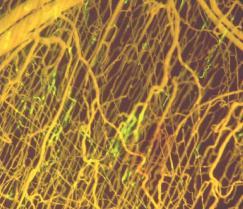
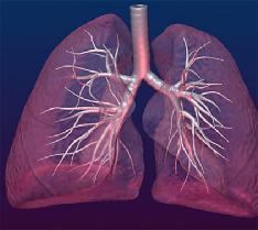
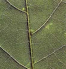
2 The micro/nanofluidic world Biological flow systems: animal blood / lung / bone capillaries, plant veins Man-made flow systems: porous solids, glass capillaries, fluidic chips

3 Comparison: nanochannel versus yeast cells 5000 nm 50 nm x 100 nm N.B. At the same scale!
4


5 Top-down approach: same principle, smaller tools from meters to millimeters to micrometers

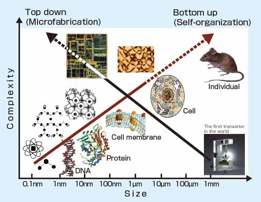
6 Top-down and bottom-up nanofabrication

7 Batchmicrofabricationprocess (IC's) MODELING AND DESIGN BACK-END PROCESSING copied from: MEMS Tutorial by M.A. Michalicek

8 The core technology: photolithography

9 Photolithography andpattern transfer

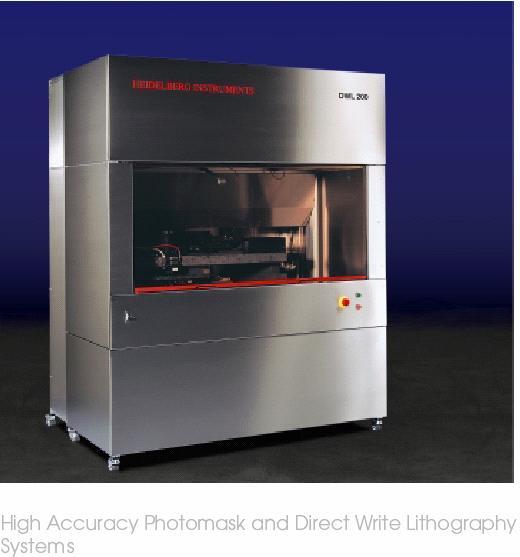
10 Typical equipment: mask aligners
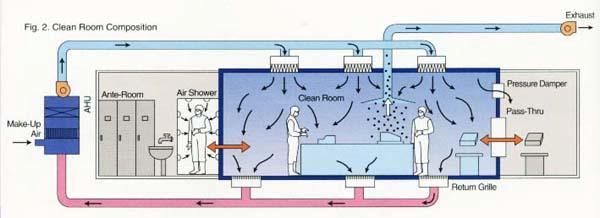
11 Working environment:clean room


 on 100 mm")

12 Computer-aided mask design A single microfluidic chip Alignment marks Microfluidic chips (3 layers) on 100 mm substrates (2 wafers) Different colours represent different material layers / processes
13 Mask fabrication e.g. by laser beam writing


14 Alignment and exposure systems Projection systems use imaging optics in between the mask and the wafer that reduce the image by a factor 4-5
15 Limitations of optical lithography Projection lithography works at Rayleigh diffraction limit. Resolution: R = k 1 λ NA NA=numerical aperture ( ) λ=wavelength k 1 depends on process ( ) Note: for these values, R λ Depth of focus: DOF = k Advanced litho: k 2 =0.7 2 λ ( NA) 2

16 Timeline optical lithography (μm) Today: M. Rothschild et al, Lincoln Lab. J. vol.14, nr.2, 2003, p.221
17 Towards optical nano lithography Lower wavelengths: deep-uv excimer lasers KrF 248 nm, ArF 193 nm, F nm* (lens/mask transmission issues) X-ray: λ 0.8 nm (synchrotron source needed) Higher contrast photoresists (theoretical limit lines & spaces: k 1 =0.25*) Improved optics & immersion lithography, i.e. liquid between lens and substrate (NA=1.3* with water; absorption issues) *R = 30 nm, DOF = 65 nm scanning beam lithography: next slide


18 Direct-write electron beamlithography At 100-keV e-beam energy, λ = 3.7 pm With typical NA 0.001, R 4 nm Limitations: charging, speed
19 Mask-less photolithography Scanning electron-beam writing -see before (also possible with focused ion beams -see after) Zone-plate array lithography Holographic (interferometric) lithography "Soft" lithography (imprint lithography)

20 Zone-plate array lithography R. Menon et al., Materials today, Feb. 2005, p. 26

21 Zone-plate array lithography (Left) Focusing principle of a zone plate. The zones are arranged such that light from adjacent zones interferes constructively at the focus. (Right) Scanning electron micrograph of the central zones of a zone plate. k 1 =0.32, NA=0.85, λ=193nm: R 70 nm R. Menon et al., Materials today, Feb. 2005, p. 26
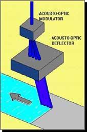
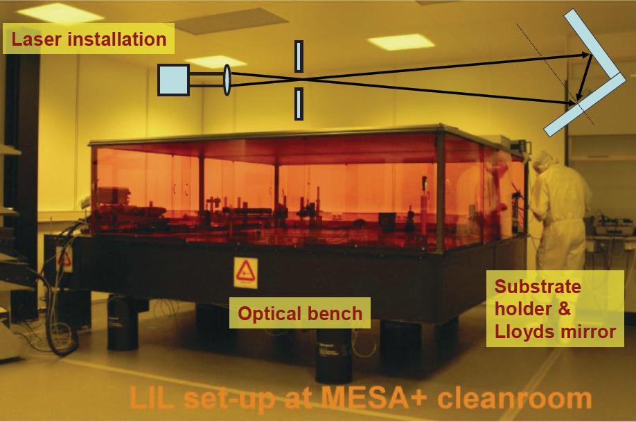
22 Laser interference lithography Principle: interference of two beams creates sinusoidal intensity gradient across substrate with photoresist. Period of interference pattern is: p λ = 2sin Θ Thus, the exposed pattern can have a pitch smaller than λ
23

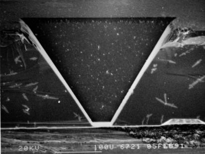
24 Some results: parallel lines in silicon R. Luttge et al., Laser interferometric nanolithography using a new positive chemical amplified resist, J. Vac. Sci. Technol. B, in press


25 Multiple exposure interference litho Change in nano-dot pattern leads to change in anisotropic wetting properties (R. Luttge, unpublished) 18 Gbit/inch 2 array of photoresist dots on sputtered platinum thin film (R. Luttge et al. J. Vac. Sci. Technol. B, in press)
 R123 R141")
26 Soft lithography concepts NIL, nano imprint lithography, uses hot embossing SFIL, step-and-flash imprint lithography, uses a liquid resist which is cross-linked by UV L.J. Guo, J. Phys. D: Appl. Phys. 37 (2004) R123 R141

27 Nano imprint lithography (NIL) hard stamp (Si) polymer (PMMA) imprint: T>T g, high p release at T<T g residual layer removal (RIE) Glassy state: no flow; rubbery state: reversible deformation; flow state: irreversible, viscous flow For NIL: flow state needed: thermoplastic, non-crosslinked polymer (e.g. PMMA or PS) Empirical rule: Imprint at 70 to 100 o C above T g

28 Example nanoimprint lithography Silicon stamp (made by e-beam) Imprint into PMMA Review: C.M. Sotomayor Torres et al. Mater. Sci. Eng. C 23, 2003, p. 23


29 Example nanoimprint lithography High resolution NIL: master in SiO 2 imprint in PMMA metal structures after lift-off S. Y. Chou, Nanoimprint Lithography, Ch. 2 in: Alternative Lithography, C.M. Sotomayor Torres, Ed. 2003, Kluwer Academic, NY


30 Nanochannels by NIL L.J. Guo e.a. Nano Lett. 4, 2004, p. 69
 hard & transparent (silica, quartz) for UV-NIL b) soft & transparent (PDMS) for \"soft UV-NIL\" Picture property of Molecular Imprints")
31 Step-and-flash imprint lithography (SFIL) imprint into low viscosity, photocurable organosilicon liquid UV flood exposure for curing stamp is: a) hard & transparent (silica, quartz) for UV-NIL b) soft & transparent (PDMS) for "soft UV-NIL" Picture property of Molecular Imprints Inc.

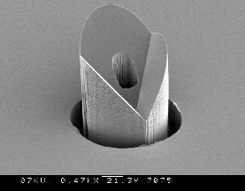
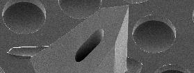
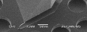
32 Resist dispensing pattern Picture property of Molecular Imprints Inc.


33 Step-and-stamp lithography Repeated imprints into PPM J. Ahopelto, T. Haatainen, Step and Stamp Imprint Lithography, Ch. 6 in: Alternative Lithography, C. M. Sotomayor Torres, Ed. 2003, Kluwer Academic, NY
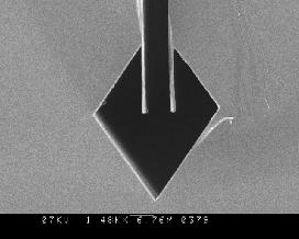
34 Microcontact printing (μcp) Example: Application of monolayers on gold pour on PDMS PDMS cure & peel off stamp master gold printing soak with ink monolayer substrate thiol or thioether ink wet etching Slide courtesy of Jurriaan Huskens, MNF, MESA+ Y. Xia and G.M. Whitesides, Angew. Chem. Int. Ed. 37, 1998, 550


35 Industrial μcp: Philips' wave printer M.M.J. Decré et al., MRS Symp. Proc. 2004, Vol. EXS-2, 59
36 Master & stamp fabrication Hard, non-transparent stamps (NIL, SSIL): Si processing (optical lithography, e-beam) Soft stamps (mcp, CFL, soft UV-NIL): hard masters via Si processing followed by replica molding Hard, transparent stamps (UV-NIL, SFIL): silica/quartz processing: fused silica with Cr and e-beam resist patterning by e-beam etching into Cr etching into silica by RIE
37 Pattern transfer: Bulkmachining General procedure: Application of a masking (protective) material Patterning of material by photolithography and selective layer etching Selective bulk etching isotropic anisotropic directional crystal plane
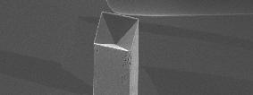
38 Example: anisotropic etching of silicon pyramidal shape


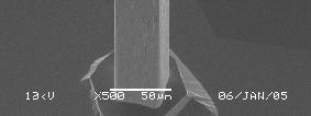
39 Example: Isotropic etching of silicon A A' A A'
")


40 Deep Reactive Ion Etching (DRIE) Principle: SF 6 gas etches the silicon O 2 gas passivates the sidewalls Isotropic or directional, depending on the settings


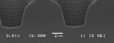
41 Deep RIE via "Bosch process" "scallops" p 700 nm


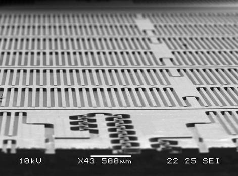
42 Focused ion beam etching 500 nm structures in ZrO 2 W.J. MoberlyChan e.a. MRS Bull. May 2007, p.424

43 Surface micromachining: basic scheme deposition of sacrificial layer patterning of sacrificial layer deposition of structural layer patterning of structural layer release etch


44 Nano needles by surface micromachining nanochannel 50nm ID Microneedles cell at 15 x 5 x 0.4 μm 3 same scale J.Emmelkamp, An integrated micro bidirectional dosing system for single cell analysis on-chip, PhD thesis, Univ. of Twente, 2007

 is 15 hrs!")
45 Nanochannels by directional etching and sacrificial layer etching Step A from: Kim e.a. Appl. Phys. Lett. 79, 2001, p.3812 Complete proces: Tas e.a. Nanolett. 2, 2002, p.1031 Etching time (L = 0.64 mm) is 15 hrs!
 for nature to remove the softer layer and")
 to remove the sacrificial layer and create the nanochannel")
46 Sacrificial layer removal requires patience It took tens of ppms of the age of the universe (i.e. million years) for nature to remove the softer layer and create the arch 100 nm It takes tens of ppms of the age of a microfabrication expert (i.e. 100,000 seconds) to remove the sacrificial layer and create the nanochannel

47 Removal of layer in microchannel width: 2 μm poly-si layer in 25 wt% KOH solution at 74 C J.W. Berenschot e.a. J. Micromech. Microeng. 12, 2002, p.621


48 Stiction caused by surface tension during drying time Review: Zhao e.a. J.Adhesion Sci.Technol.17, (2003) Theoretical model: Mastrangelo e.a J.MEMS 2, 44 (1993)

49 Maximum dimensions without stiction L max = 3Et 8 3 W a h For other structures: L max, w max, R P max = 2 b + b + 2 4c 1 2 ν: Poisson's ratio σ R : residual stress E: Young's modulus L, w, R P are the length of the doubly clamped beam, width of the square plate and radius of the circular plate, respectively Zhao e.a. J.Adhesion Sci.Technol.17, (2003)


50 How to use stiction Tas e.a. Nanolett. 2, 2002, p.1031 Etching time is 4 min.


51 Nanochannels by etching and sealing a b Void formation in a 6-μm-thick BPSG glass layer deposited over template ridges with h=6.4μm, w=4μm and d=3μm: a. as deposited, b. and c. annealed at 1050 C for 4 and 12 hrs, resp. Annealing causes reflow of the glass layer Callender e.a. J. Mater. Res. 20, 2005, p. 759 c


52 Nanochannels by etching and sealing bonded surface height 50 nm J. Haneveld e.a. J. Micromech. Microeng. 13, 2003, p. S62
53 Channels with integrated electrodes Electrode deposition Deposition silica insulation CMP Channel etching Direct bonding E.J. van der Wouden e.a. Coll. Surf. A 267, 2005, p. 110

")
54 Chemical mechanical polishing, CMP Effects of CMP: Reduction of roughness Surface (chemical) conditioning Planarization
 drawing fiber from liquid polymer droplet (B) attaching drawn fiber into second droplet to complete a suspended beam (C) alternative to (B): drawing multiple suspended fibers in parallel (D)")
55 Nanochannels by assembly Fabrication methods for forming and using polymer fibers. (A) drawing fiber from liquid polymer droplet (B) attaching drawn fiber into second droplet to complete a suspended beam (C) alternative to (B): drawing multiple suspended fibers in parallel (D) overcoating polymer network (E) dissolution of the polymer to produce a suspended capillary network Harfenist e.a. Nanolett. 4, 2004, p.1931
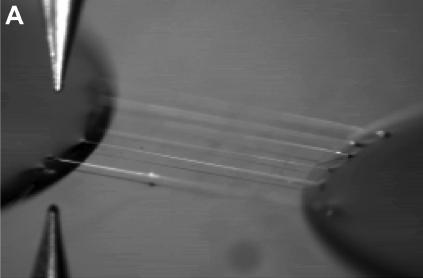
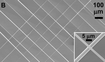
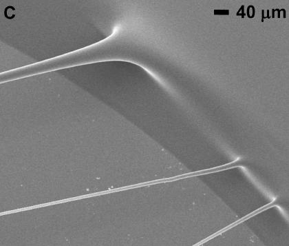
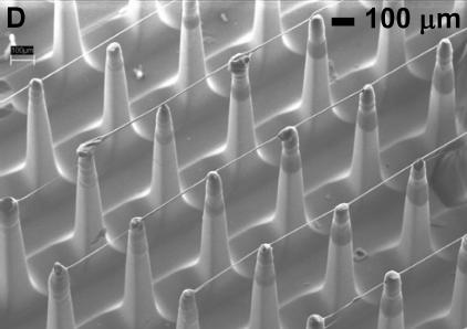
56 Nanofluidic interconnections Harfenist e.a. Nanolett. 4, 2004, p.1931


57 Nanofluidic interconnections Harfenist e.a. Nanolett. 4, 2004, p.1931


58 Bottom-up nanotechnology: atomic/molecular assembly using AFM Left: Dip-pen Right: Fountain pen Confinement of electrons to "quantum corrals" on a metal surface, using STM AFM with electrophoretic control of molecules R.D. Piner e.a. Science 283, 1999, p. 661 S. Deladi e.a. Appl. Phys. Lett. 85, 2004, p K. Unal e.a. Appl. Phys. Lett. 88, 2006, p M.F. Crommie a.a., Science 262, 1993, p.218
 uniform single-crystal")
 radial nanowire heterostructures. C.M.")
59 Nanowires and nanotubes VLS mechanism Growth and representative structures of (a) uniform single-crystal semiconductor nanowires, (b) axial nanowire heterostructures, and (c) radial nanowire heterostructures. C.M. Lieber, MRS Bulletin July 2003, p. 486

60 Carbon nanotubes Image sequence of a growing carbon nanofibre. The images are acquired with TEM in situ with CH 4 :H 2 = 1:1, total pressure 2.1 mbar, sample heated to 536 C. Scale bar, 5nm. Atomic-scale imaging of carbon nanofibre growth S. Helveg et al., Nature 427, (2004)

61 Liquid-filled carbon nanotube Low magnification TEM micrographs showing a liquid plug in the nanotube. Y. Gogotsi et al. Chem. Phys. Lett. 365 (2002) 354

62 Nanopores by anodization: silicon porous polishing/isotropic etching


63 Procedure and examples Asymmetric pores in a silicon membrane acting as massively parallel brownian ratchets, S. Matthias & F. Müller, Nature 424, (2003)


64 Self-organization of pores in anodization of aluminum Self-organization: mechanical stress induced, see A.-P. Li e.a., J. Appl. Phys. 84, 1998, p Cross-section picture: A. Cai e.a., Nanotechnology 13, 2002, p


65 Self-assembly in block co-polymers Diagram of microdomain morphologies of diblock copolymers, for varying volume fraction of components. Morphologies range from spherical (S) to cylindrical (C) to gyroid (G) to lamellar (L). The molecular weight of the block copolymer dictates the size of the microdomains, typically 10 nm. From C.J. Hawker e.a., MRS Bull. Dec. 2005, p.952 Examples from M. Park e.a. Science 276, 1997, p. 1401


66 Self-assembly of lipids hydrophilic head hydrophobic tail forms lipid bilayer (membrane) lipid vesicle M. Masuda & T. Shimizu, Lipid nanotubes and microtubes, Langmuir 20, 2004, p.5969


67 Lipid vesicles and nanotubes Microscopic liposome networks, filled with fluorescent dyes. Scale bars 10 μm. A. Karlsson e.a., Nature 409, 2001,150 Formation of nanotube-vesicle networks. vesicle: 5 to 30 μm diameter, separation distance: 10 and 100 μm, nanotube diameter: nm. A. Karlsson e.a. Anal. Chem. 75, 2003, p.2529
68 Summary fabrication methods WRITING REPLICATION remove (cut) add (dispense) modify (burn) dig - glue -fry molding / imprinting modification SELF-ORGANIZATION material transport self-assembly self-organized template interference/ standing wave photons -atoms -ions -molecules particles - gels - melts
CURRENT STATUS OF NANOIMPRINT LITHOGRAPHY DEVELOPMENT IN CNMM
 U.S. -KOREA Forums on Nanotechnology 1 CURRENT STATUS OF NANOIMPRINT LITHOGRAPHY DEVELOPMENT IN CNMM February 17 th 2005 Eung-Sug Lee,Jun-Ho Jeong Korea Institute of Machinery & Materials U.S. -KOREA Forums
Overview of the main nano-lithography techniques
 Overview of the main nano-lithography techniques Soraya Sangiao sangiao@unizar.es Outline Introduction: Nanotechnology. Nano-lithography techniques: Masked lithography techniques: Photolithography. X-ray
NPTEL. Instability and Patterning of Thin Polymer Films - Video course. Chemical Engineering.
 NPTEL Syllabus Instability and Patterning of Thin Polymer Films - Video course COURSE OUTLINE T h i s course will expose students to the science of sub-micron, meso and nanoscale patterning of surfaces
Unconventional Nano-patterning. Peilin Chen
 Unconventional Nano-patterning Peilin Chen Reference Outlines History of patterning Traditional Nano-patterning Unconventional Nano-patterning Ancient Patterning "This is the Elks' land". A greeting at
Techniken der Oberflächenphysik (Techniques of Surface Physics)
") Techniken der Oberflächenphysik (Techniques of Surface Physics) Prof. Yong Lei & Dr. Yang Xu (& Liying Liang) Fachgebiet 3D-Nanostrukturierung, Institut für Physik Contact: yong.lei@tu-ilmenau.de; yang.xu@tu-ilmenau.de;
Techniken der Oberflächenphysik (Techniques of Surface Physics) Prof. Yong Lei & Dr. Yang Xu (& Liying Liang) Fachgebiet 3D-Nanostrukturierung, Institut für Physik Contact: yong.lei@tu-ilmenau.de; yang.xu@tu-ilmenau.de;
There's Plenty of Room at the Bottom
 There's Plenty of Room at the Bottom 12/29/1959 Feynman asked why not put the entire Encyclopedia Britannica (24 volumes) on a pin head (requires atomic scale recording). He proposed to use electron microscope
Three Approaches for Nanopatterning
 Three Approaches for Nanopatterning Lithography allows the design of arbitrary pattern geometry but maybe high cost and low throughput Self-Assembly offers high throughput and low cost but limited selections
Nano Materials. Nanomaterials
 Nano Materials 1 Contents Introduction Basics Synthesis of Nano Materials Fabrication of Nano Structure Nano Characterization Properties and Applications 2 Fabrication of Nano Structure Lithographic techniques
MSN551 LITHOGRAPHY II
 MSN551 Introduction to Micro and Nano Fabrication LITHOGRAPHY II E-Beam, Focused Ion Beam and Soft Lithography Why need electron beam lithography? Smaller features are required By electronics industry:
Nanotechnology Fabrication Methods.
 Nanotechnology Fabrication Methods. 10 / 05 / 2016 1 Summary: 1.Introduction to Nanotechnology:...3 2.Nanotechnology Fabrication Methods:...5 2.1.Top-down Methods:...7 2.2.Bottom-up Methods:...16 3.Conclusions:...19
Emerging nanopatterning
 Nanotechnology for engineers Winter semester 2006-2007 Emerging nanopatterning Soft-lithography: Microcontact printing Nanoimprint Lithography Stencil lithography Dip-Pen lithography / Nanoscale dispensing
Introduction to Photolithography
 http://www.ichaus.de/news/72 Introduction to Photolithography Photolithography The following slides present an outline of the process by which integrated circuits are made, of which photolithography is
Technologies VII. Alternative Lithographic PROCEEDINGS OF SPIE. Douglas J. Resnick Christopher Bencher. Sponsored by. Cosponsored by.
 PROCEEDINGS OF SPIE Alternative Lithographic Technologies VII Douglas J. Resnick Christopher Bencher Editors 23-26 February 2015 San Jose, California, United States Sponsored by SPIE Cosponsored by DNS
MICRO AND NANOPROCESSING TECHNOLOGIES
 LECTURE 5 MICRO AND NANOPROCESSING TECHNOLOGIES Introduction Ion lithography X-ray lithography Soft lithography E-beam lithography Concepts and processes Lithography systems Masks and resists Chapt.9.
Fabrication at the nanoscale for nanophotonics
 Fabrication at the nanoscale for nanophotonics Ilya Sychugov, KTH Materials Physics, Kista silicon nanocrystal by electron beam induced deposition lithography Outline of basic nanofabrication methods Devices
Supplementary Figure 1 Detailed illustration on the fabrication process of templatestripped
 Supplementary Figure 1 Detailed illustration on the fabrication process of templatestripped gold substrate. (a) Spin coating of hydrogen silsesquioxane (HSQ) resist onto the silicon substrate with a thickness
Lecture 18: Microfluidic MEMS, Applications
 MECH 466 Microelectromechanical Systems University of Victoria Dept. of Mechanical Engineering Lecture 18: Microfluidic MEMS, Applications 1 Overview Microfluidic Electrokinetic Flow Basic Microfluidic
Nanotechnology Nanofabrication of Functional Materials. Marin Alexe Max Planck Institute of Microstructure Physics, Halle - Germany
 Nanotechnology Nanofabrication of Functional Materials Marin Alexe Max Planck Institute of Microstructure Physics, Halle - Germany Contents Part I History and background to nanotechnology Nanoworld Nanoelectronics
Micro/nano and precision manufacturing technologies and applications
 The 4th China-American Frontiers of Engineering Symposium Micro/nano and precision manufacturing technologies and applications Dazhi Wang School of Mechanical Engineering Dalian University of Technology
Nanostructures Fabrication Methods
 Nanostructures Fabrication Methods bottom-up methods ( atom by atom ) In the bottom-up approach, atoms, molecules and even nanoparticles themselves can be used as the building blocks for the creation of
Kavli Workshop for Journalists. June 13th, CNF Cleanroom Activities
 Kavli Workshop for Journalists June 13th, 2007 CNF Cleanroom Activities Seeing nm-sized Objects with an SEM Lab experience: Scanning Electron Microscopy Equipment: Zeiss Supra 55VP Scanning electron microscopes
Fabrication of micro-optical components in polymer using proton beam micro-machining and modification
 Nuclear Instruments and Methods in Physics Research B 210 (2003) 250 255 www.elsevier.com/locate/nimb Fabrication of micro-optical components in polymer using proton beam micro-machining and modification
High-density data storage: principle
 High-density data storage: principle Current approach High density 1 bit = many domains Information storage driven by domain wall shifts 1 bit = 1 magnetic nanoobject Single-domain needed Single easy axis
EE C245 ME C218 Introduction to MEMS Design Fall 2007
 EE C245 ME C218 Introduction to MEMS Design Fall 2007 Prof. Clark T.-C. Nguyen Dept. of Electrical Engineering & Computer Sciences University of California at Berkeley Berkeley, CA 94720 Lecture 11: Bulk
Top down and bottom up fabrication
 Lecture 24 Top down and bottom up fabrication Lithography ( lithos stone / graphein to write) City of words lithograph h (Vito Acconci, 1999) 1930 s lithography press Photolithography d 2( NA) NA=numerical
UNIT 3. By: Ajay Kumar Gautam Asst. Prof. Dev Bhoomi Institute of Technology & Engineering, Dehradun
 UNIT 3 By: Ajay Kumar Gautam Asst. Prof. Dev Bhoomi Institute of Technology & Engineering, Dehradun 1 Syllabus Lithography: photolithography and pattern transfer, Optical and non optical lithography, electron,
Nanoimprint Lithography
 Nanoimprint Lithography Wei Wu Quantum Science Research Advanced Studies HP Labs, Hewlett-Packard Email: wei.wu@hp.com Outline Background Nanoimprint lithography Thermal based UV-based Applications based
Supplementary information for
 Supplementary information for Transverse electric field dragging of DNA in a nanochannel Makusu Tsutsui, Yuhui He, Masayuki Furuhashi, Rahong Sakon, Masateru Taniguchi & Tomoji Kawai The Supplementary
Fabrication of ordered array at a nanoscopic level: context
 Fabrication of ordered array at a nanoscopic level: context Top-down method Bottom-up method Classical lithography techniques Fast processes Size limitations it ti E-beam techniques Small sizes Slow processes
Lecture 14 Advanced Photolithography
 Lecture 14 Advanced Photolithography Chapter 14 Wolf and Tauber 1/74 Announcements Term Paper: You are expected to produce a 4-5 page term paper on a selected topic (from a list). Term paper contributes
Nanolithography Techniques
 Nanolithography Techniques MSE 505 / MSNT 505 P. Coane Outline What Is Nanotechnology? The Motivation For Going Small Nanofabrication Technologies Basic Techniques Nano Lithography NANOTECHNOLOGY Nanotechnology
ABSTRACT. Dr. Donald L. DeVoe, Associate Professor, Department of Mechanical Engineering
 ABSTRACT Title of Document: NANOCHANNEL FABRICATION USING THERMOMECHANICAL DEFORMATION OF THERMOPLASTICS Kapil Sahasrabudhe, M.S. Mechanical Engineering, September 2006 Directed By: Dr. Donald L. DeVoe,
A Novel Self-aligned and Maskless Process for Formation of Highly Uniform Arrays of Nanoholes and Nanopillars
 Nanoscale Res Lett (2008) 3: 127 DOI 10.1007/s11671-008-9124-6 NANO EXPRESS A Novel Self-aligned and Maskless Process for Formation of Highly Uniform Arrays of Nanoholes and Nanopillars Wei Wu Æ Dibyendu
29: Nanotechnology. What is Nanotechnology? Properties Control and Understanding. Nanomaterials
 29: Nanotechnology What is Nanotechnology? Properties Control and Understanding Nanomaterials Making nanomaterials Seeing at the nanoscale Quantum Dots Carbon Nanotubes Biology at the Nanoscale Some Applications
Figure 1: Some examples of objects at different size scales ( 2001, CMP Científica, [2])
![Figure 1: Some examples of objects at different size scales ( 2001, CMP Científica, [2])](/thumbs/85/91872790.jpg "Figure 1: Some examples of objects at different size scales ( 2001, CMP Científica, [2])") Top-Down vs. Bottom-Up Nanomanufacturing Prof. Derek J. Hansford, Biomedical Engineering Program and Department of Materials Science & Engineering Learning Objectives: This module should expose the student
Top-Down vs. Bottom-Up Nanomanufacturing Prof. Derek J. Hansford, Biomedical Engineering Program and Department of Materials Science & Engineering Learning Objectives: This module should expose the student
Wafer bonding. Supplementary Figure 1. Conventional nanofluidic sealing process. (a) Selective sealing. (b) Wafer bonding. (c) Sacrificial etching.
 Selective sealing. (b) Wafer bonding. (c) Sacrificial etching.") (a) (b) (c) Selective sealing Wafer bonding Sacrificial etching Supplementary Figure 1. Conventional nanofluidic sealing process. (a) Selective sealing. (b) Wafer bonding. (c) Sacrificial etching. Supplementary
(a) (b) (c) Selective sealing Wafer bonding Sacrificial etching Supplementary Figure 1. Conventional nanofluidic sealing process. (a) Selective sealing. (b) Wafer bonding. (c) Sacrificial etching. Supplementary
Lecture Topic B
 Lecture 08.11.2010 Topic B Surface Engineering Au, Cu, Ag Al2O3 HS-R (OH)3-P-O-R SiO2 X3Si-O-R Tailored Surface Chemistry Micro-contact printing Polymer stamp (PDMS) Siliconmicrostructure or PMMA resist
Photolithography 光刻 Part II: Photoresists
 微纳光电子材料与器件工艺原理 Photolithography 光刻 Part II: Photoresists Xing Sheng 盛兴 Department of Electronic Engineering Tsinghua University xingsheng@tsinghua.edu.cn 1 Photolithography 光刻胶 负胶 正胶 4 Photolithography
process dependencies in nanoimprint
 Modeling and mitigating pattern and process dependencies in nanoimprint lithography 23 June 2011 Hayden Taylor Singapore-MIT Alliance for Research and Technology formerly based at: Microsystems Technology
Figure 1: Graphene release, transfer and stacking processes. The graphene stacking began with CVD
 Supplementary figure 1 Graphene Growth and Transfer Graphene PMMA FeCl 3 DI water Copper foil CVD growth Back side etch PMMA coating Copper etch in 0.25M FeCl 3 DI water rinse 1 st transfer DI water 1:10
Supplementary Information
 ature anotechnology reference number: AO-06110617A Growth and alignment of polyaniline nanofibres with superhydrophobic, superhydrophilic and other properties an-rong Chiou 1,2,3, Chunmeng Lu 1, Jingjiao
Nanostructured Materials - Fabrication Processes 1
 FABRICATION PROCESSES FOR NANOMATERIALS - NANOSTRUCTURES Lecture 6 1 Processes 1 SUBTRACTIVE AND MODIFYING METHODS Subtractive methods: Etching: wet chemical etching, reactive ion etching; ion beam sputter
Nanomaterials and their Optical Applications
 Nanomaterials and their Optical Applications Winter Semester 2013 Lecture 02 rachel.grange@uni-jena.de http://www.iap.uni-jena.de/multiphoton Lecture 2: outline 2 Introduction to Nanophotonics Theoretical
Thin Wafer Handling Challenges and Emerging Solutions
 1 Thin Wafer Handling Challenges and Emerging Solutions Dr. Shari Farrens, Mr. Pete Bisson, Mr. Sumant Sood and Mr. James Hermanowski SUSS MicroTec, 228 Suss Drive, Waterbury Center, VT 05655, USA 2 Thin
High-resolution Characterization of Organic Ultrathin Films Using Atomic Force Microscopy
 High-resolution Characterization of Organic Ultrathin Films Using Atomic Force Microscopy Jing-jiang Yu Nanotechnology Measurements Division Agilent Technologies, Inc. Atomic Force Microscopy High-Resolution
Nano-Lithography. Edited by Stefan Landis
 Nano-Lithography Edited by Stefan Landis IST^ m WILEY Table of Contents Foreword Jörge DE SOUSA NORONHA Introduction Michel BRILLOUET xi xvii Chapter 1. X-ray Lithography: Fundamentals and Applications
Self-study problems and questions Processing and Device Technology, FFF110/FYSD13
 Self-study problems and questions Processing and Device Technology, FFF110/FYSD13 Version 2016_01 In addition to the problems discussed at the seminars and at the lectures, you can use this set of problems
Dip-Pen Lithography 1
 Dip-Pen Lithography 1 A Brief History of Writing Instruments From Quills and Bamboos to fountain pens and brushes M. Klein and Henry W. Wynne received US patent #68445 in 1867 for an ink chamber and delivery
MEEN Nanoscale Issues in Manufacturing. Lithography Lecture 1: The Lithographic Process
 MEEN 489-500 Nanoscale Issues in Manufacturing Lithography Lecture 1: The Lithographic Process 1 Discuss Reading Assignment 1 1 Introducing Nano 2 2 Size Matters 3 3 Interlude One-The Fundamental Science
EE C245 ME C218 Introduction to MEMS Design Fall 2007
 EE C245 ME C218 Introduction to MEMS Design Fall 2007 Prof. Clark T.-C. Nguyen Dept. of Electrical Engineering & Computer Sciences University of California at Berkeley Berkeley, CA 94720 Lecture 12: Mechanics
Introduction. Photoresist : Type: Structure:
 Photoresist SEM images of the morphologies of meso structures and nanopatterns on (a) a positively nanopatterned silicon mold, and (b) a negatively nanopatterned silicon mold. Introduction Photoresist
Lithography Challenges Moore s Law Rising Costs and Challenges of Advanced Patterning
 Lithography Challenges Moore s Law Rising Costs and Challenges of Advanced Patterning SEMI Texas Spring Forum May 21, 2013 Austin, Texas Author / Company / Division / Rev. / Date A smartphone today has
Nano fabrication and optical characterization of nanostructures
 Introduction to nanooptics, Summer Term 2012, Abbe School of Photonics, FSU Jena, Prof. Thomas Pertsch Nano fabrication and optical characterization of nanostructures Lecture 12 1 Optical characterization
Fabrication and application of a full wafer size micro/ nanostencil for multiple length-scale surface patterning
 Microelectronic Engineering 67 68 (2003) 609 614 www.elsevier.com/ locate/ mee Fabrication and application of a full wafer size micro/ nanostencil for multiple length-scale surface patterning 1 * G.M.
Liquid nanodispensing
 Liquid nanodispensing Thierry Ondarçuhu, Laure Fabié, Erik Dujardin, Aiping Fang Nanosciences group, CEMES-CNRS, Toulouse (France) Nanopatterning, molecule deposition Dynamics of liquids at sub-micron
Presentation Phys Katia GASPERI. Statistical study of single DNA molecules into dynamic array
 Presentation Phys 730 - Katia GASPERI Statistical study of single DNA molecules into dynamic array 1 Statistical study of single DNA molecules into dynamic array - Research project lead by Laurence SALOME
Highly Sensitive Color-Tunablility by Scalable. Nanomorphology of Dielectric Layer in Liquid Permeable. Metal-Insulator-Metal Structure
 Supporting Information Highly Sensitive Color-Tunablility by Scalable Nanomorphology of Dielectric Layer in Liquid Permeable Metal-Insulator-Metal Structure Eui-Sang Yu,, Sin-Hyung Lee, Young-Gyu Bae,
Photolithography II ( Part 1 )
") 1 Photolithography II ( Part 1 ) Chapter 14 : Semiconductor Manufacturing Technology by M. Quirk & J. Serda Bjørn-Ove Fimland, Department of Electronics and Telecommunication, Norwegian University of Science
1 Photolithography II ( Part 1 ) Chapter 14 : Semiconductor Manufacturing Technology by M. Quirk & J. Serda Bjørn-Ove Fimland, Department of Electronics and Telecommunication, Norwegian University of Science
EE 527 MICROFABRICATION. Lecture 25 Tai-Chang Chen University of Washington
 EE 527 MICROFABRICATION Lecture 25 Tai-Chang Chen University of Washington ION MILLING SYSTEM Kaufmann source Use e-beam to strike plasma A magnetic field applied to increase ion density Drawback Low etch
Providing sustainable supply of clean water is one of
 1 Introduction Fabrication of Water Treatment Membrane Using Templating Method A Critical Review Fabrication of Water Treatment Membrane Using Templating Method A Critical Review ABSTRACT The progress
Deposition of Multilayer Fibers and Beads by Near-Field Electrospinning for Texturing and 3D Printing Applications
 Deposition of Multilayer Fibers and Beads by Near-Field Electrospinning for Texturing and 3D Printing Applications Nicolas Martinez-Prieto, Jian Cao, and Kornel Ehmann Northwestern University SmartManufacturingSeries.com
ESS 5855 Surface Engineering for. MicroElectroMechanicalechanical Systems. Fall 2010
 ESS 5855 Surface Engineering for Microelectromechanical Systems Fall 2010 MicroElectroMechanicalechanical Systems Miniaturized systems with integrated electrical and mechanical components for actuation
Presentation Phys Katia GASPERI. Statistical study of single DNA molecules into dynamic array
 Presentation Phys 730 - Katia GASPERI Statistical study of single DNA molecules into dynamic array 1 Statistical study of single DNA molecules into dynamic array - Research project lead by Laurence SALOME
NANONICS IMAGING FOUNTAIN PEN
 NANONICS IMAGING FOUNTAIN PEN NanoLithography Systems Methods of Nanochemical Lithography Fountain Pen NanoLithography A. Lewis et al. Appl. Phys. Lett. 75, 2689 (1999) FPN controlled etching of chrome.
Regents of the University of California
 Deep Reactive-Ion Etching (DRIE) DRIE Issues: Etch Rate Variance The Bosch process: Inductively-coupled plasma Etch Rate: 1.5-4 μm/min Two main cycles in the etch: Etch cycle (5-15 s): SF 6 (SF x+ ) etches
The fabrication of periodic metal nanodot arrays through pulsed laser melting induced fragmentation of metal nanogratings
 IOP PUBLISHING Nanotechnology 20 (2009) 285310 (5pp) NANOTECHNOLOGY doi:10.1088/0957-4484/20/28/285310 The fabrication of periodic metal nanodot arrays through pulsed laser melting induced fragmentation
DQN Positive Photoresist
 UNIVESITY OF CALIFONIA, BEKELEY BEKELEY DAVIS IVINE LOS ANGELES IVESIDE SAN DIEGO SAN FANCISCO SANTA BABAA SANTA CUZ DEPATMENT OF BIOENGINEEING 94720-1762 BioE 121 Midterm #1 Solutions BEKELEY, CALIFONIA
Highly charged ion beams applied to fabrication of Nano-scale 3D structures. Sadao MOMOTA Kochi University of Technology
 Highly charged ion beams applied to fabrication of Nano-scale 3D structures Sadao MOMOTA Kochi University of Technology Introduction 1 Prospect of microscopic structures 2D Semiconductor 3D Ex. MEMS http://www.rise.waseda.ac.jp/proj/sci/s98s08/j-s98s08.html
Outline. 1 Introduction. 2 Basic IC fabrication processes. 3 Fabrication techniques for MEMS. 4 Applications. 5 Mechanics issues on MEMS MDL NTHU
 Outline 1 Introduction 2 Basic IC fabrication processes 3 Fabrication techniques for MEMS 4 Applications 5 Mechanics issues on MEMS 2. Basic IC fabrication processes 2.1 Deposition and growth 2.2 Photolithography
ME381 Introduction to MEMS
 ME381 Introduction to MEMS Term Project Dynamic Wettability Switching by Surface Roughness Effect Bo He Hang Cheng Hongzhou Jiang December 6 th, 2002 1 TABLE OF CONTENTS Abstract........1 Introduction......1
Towards nanoimprint lithography-aware layout design checking. 25 February 2010 Hayden Taylor and Duane Boning Massachusetts Institute of Technology
 Towards nanoimprint lithography-aware layout design checking 25 February 2010 Hayden Taylor and Duane Boning Massachusetts Institute of Technology Nanoimprint is the mechanical patterning of resist spun
EE C247B / ME C218 INTRODUCTION TO MEMS DESIGN SPRING 2016 C. NGUYEN PROBLEM SET #4
 Issued: Wednesday, March 4, 2016 PROBLEM SET #4 Due: Monday, March 14, 2016, 8:00 a.m. in the EE C247B homework box near 125 Cory. 1. This problem considers bending of a simple cantilever and several methods
Chapter 2 FABRICATION PROCEDURE AND TESTING SETUP. Our group has been working on the III-V epitaxy light emitting materials which could be
 Chapter 2 7 FABRICATION PROCEDURE AND TESTING SETUP 2.1 Introduction In this chapter, the fabrication procedures and the testing setups for the sub-micrometer lasers, the submicron disk laser and the photonic
Supplementary Information. Light Manipulation for Organic Optoelectronics Using Bio-inspired Moth's Eye. Nanostructures
 Supplementary Information Light Manipulation for Organic Optoelectronics Using Bio-inspired Moth's Eye Nanostructures Lei Zhou, Qing-Dong Ou, Jing-De Chen, Su Shen, Jian-Xin Tang,* Yan-Qing Li,* and Shuit-Tong
Lithography and Etching
 Lithography and Etching Victor Ovchinnikov Chapters 8.1, 8.4, 9, 11 Previous lecture Microdevices Main processes: Thin film deposition Patterning (lithography) Doping Materials: Single crystal (monocrystal)
Lecture 3. Self-assembled Monolayers (SAM)
") 10.524 Lecture 3. Self-assembled Monolayers (SAM) Instructor: Prof. Zhiyong Gu (Chemical Engineering & UML CHN/NCOE Nanomanufacturing Center) Lecture 3: Self-assembled Monolayers (SAMs) Table of Contents
10.524 Lecture 3. Self-assembled Monolayers (SAM) Instructor: Prof. Zhiyong Gu (Chemical Engineering & UML CHN/NCOE Nanomanufacturing Center) Lecture 3: Self-assembled Monolayers (SAMs) Table of Contents
Scanning Tunneling Microscopy
 Scanning Tunneling Microscopy References: 1. G. Binnig, H. Rohrer, C. Gerber, and Weibel, Phys. Rev. Lett. 49, 57 (1982); and ibid 50, 120 (1983). 2. J. Chen, Introduction to Scanning Tunneling Microscopy,
Nanostrukturphysik (Nanostructure Physics)
") Nanostrukturphysik (Nanostructure Physics) Prof. Yong Lei & Dr. Yang Xu Fachgebiet 3D-Nanostrukturierung, Institut für Physik Contact: yong.lei@tu-ilmenau.de; yang.xu@tu-ilmenau.de Office: Unterpoerlitzer
Nanostrukturphysik (Nanostructure Physics) Prof. Yong Lei & Dr. Yang Xu Fachgebiet 3D-Nanostrukturierung, Institut für Physik Contact: yong.lei@tu-ilmenau.de; yang.xu@tu-ilmenau.de Office: Unterpoerlitzer
Formation and Surface Modification of Nanopatterned Thiol-ene Substrates using
 Supporting Information Formation and Surface Modification of Nanopatterned Thiol-ene Substrates using Step and Flash Imprint Lithography Vaibhav S. Khire, 1 Youngwoo Yi, 2 Noel A. Clark, 2 and Christopher
SUPPLEMENTARY NOTES Supplementary Note 1: Fabrication of Scanning Thermal Microscopy Probes
 SUPPLEMENTARY NOTES Supplementary Note 1: Fabrication of Scanning Thermal Microscopy Probes Fabrication of the scanning thermal microscopy (SThM) probes is summarized in Supplementary Fig. 1 and proceeds
ALIGNMENT ACCURACY IN A MA/BA8 GEN3 USING SUBSTRATE CONFORMAL IMPRINT LITHOGRAPHY (SCIL)
") ALIGNMENT ACCURACY IN A MA/BA8 GEN3 USING SUBSTRATE CONFORMAL IMPRINT LITHOGRAPHY (SCIL) Robert Fader Fraunhofer Institute for Integrated Systems and Device Technology (IISB) Germany Ulrike Schömbs SUSS
ALIGNMENT ACCURACY IN A MA/BA8 GEN3 USING SUBSTRATE CONFORMAL IMPRINT LITHOGRAPHY (SCIL) Robert Fader Fraunhofer Institute for Integrated Systems and Device Technology (IISB) Germany Ulrike Schömbs SUSS
Nanotechnology. Gavin Lawes Department of Physics and Astronomy
 Nanotechnology Gavin Lawes Department of Physics and Astronomy Earth-Moon distance 4x10 8 m (courtesy NASA) Length scales (Part I) Person 2m Magnetic nanoparticle 5x10⁻⁹ m 10 10 m 10 5 m 1 m 10-5 m 10-10
Nova 600 NanoLab Dual beam Focused Ion Beam IITKanpur
 Nova 600 NanoLab Dual beam Focused Ion Beam system @ IITKanpur Dual Beam Nova 600 Nano Lab From FEI company (Dual Beam = SEM + FIB) SEM: The Electron Beam for SEM Field Emission Electron Gun Energy : 500
Nanostructure. Materials Growth Characterization Fabrication. More see Waser, chapter 2
 Nanostructure Materials Growth Characterization Fabrication More see Waser, chapter 2 Materials growth - deposition deposition gas solid Physical Vapor Deposition Chemical Vapor Deposition Physical Vapor
I. NANOFABRICATION O AND CHARACTERIZATION Chap. 2 : Self-Assembly
 I. Nanofabrication and Characterization : TOC I. NANOFABRICATION O AND CHARACTERIZATION Chap. 1 : Nanolithography Chap. 2 : Self-Assembly Chap. 3 : Scanning Probe Microscopy Nanoscale fabrication requirements
Self-assembled nanostructures for antireflection optical coatings
 Self-assembled nanostructures for antireflection optical coatings Yang Zhao 1, Guangzhao Mao 2, and Jinsong Wang 1 1. Deaprtment of Electrical and Computer Engineering 2. Departmentof Chemical Engineering
EE 527 MICROFABRICATION. Lecture 24 Tai-Chang Chen University of Washington
 EE 527 MICROFABRICATION Lecture 24 Tai-Chang Chen University of Washington EDP ETCHING OF SILICON - 1 Ethylene Diamine Pyrocatechol Anisotropy: (100):(111) ~ 35:1 EDP is very corrosive, very carcinogenic,
Imaging Methods: Scanning Force Microscopy (SFM / AFM)
") Imaging Methods: Scanning Force Microscopy (SFM / AFM) The atomic force microscope (AFM) probes the surface of a sample with a sharp tip, a couple of microns long and often less than 100 Å in diameter.
Imaging Methods: Scanning Force Microscopy (SFM / AFM) The atomic force microscope (AFM) probes the surface of a sample with a sharp tip, a couple of microns long and often less than 100 Å in diameter.
EE 143 MICROFABRICATION TECHNOLOGY FALL 2014 C. Nguyen PROBLEM SET #7. Due: Friday, Oct. 24, 2014, 8:00 a.m. in the EE 143 homework box near 140 Cory
 Issued: Tuesday, Oct. 14, 2014 PROBLEM SET #7 Due: Friday, Oct. 24, 2014, 8:00 a.m. in the EE 143 homework box near 140 Cory Electroplating 1. Suppose you want to fabricate MEMS clamped-clamped beam structures
Microfabrication for MEMS: Part I
 Microfabrication for MEMS: Part I Carol Livermore Massachusetts Institute of Technology * With thanks to Steve Senturia, from whose lecture notes some of these materials are adapted. CL: 6.777J/2.372J
Soft Lithography and Materials Properties in MEMS
 CL: 6.777J/2.372J Spring 2007, Lecture 5-1 Soft Lithography and Materials Properties in MEMS Carol Livermore Massachusetts Institute of Technology * With thanks to Steve Senturia and Joel Voldman, from
Etching Capabilities at Harvard CNS. March 2008
 Etching Capabilities at Harvard CNS March 2008 CNS: A shared use facility for the Harvard Community and New England CNS Provides technical support, equipment and staff. Explicitly multi-disciplinary w/
Fabrication of micromachined fountain pen with in situ characterization possibility of nanoscale surface modification
 INSTITUTE OFPHYSICS PUBLISHING JOURNAL OFMICROMECHANICS ANDMICROENGINEERING J. Micromech. Microeng. 15 (2005) 528 534 doi:10.1088/0960-1317/15/3/013 Fabrication of micromachined fountain pen with in situ
Tilted ion implantation as a cost-efficient sublithographic
 Tilted ion implantation as a cost-efficient sublithographic patterning technique Sang Wan Kim 1,a), Peng Zheng 1, Kimihiko Kato 1, Leonard Rubin 2, Tsu-Jae King Liu 1 1 Department of Electrical Engineering
Supporting Information. Fast Synthesis of High-Performance Graphene by Rapid Thermal Chemical Vapor Deposition
 1 Supporting Information Fast Synthesis of High-Performance Graphene by Rapid Thermal Chemical Vapor Deposition Jaechul Ryu, 1,2, Youngsoo Kim, 4, Dongkwan Won, 1 Nayoung Kim, 1 Jin Sung Park, 1 Eun-Kyu
Nanostructured substrate with nanoparticles fabricated by femtosecond laser for surface-enhanced Raman scattering
 Nanostructured substrate with nanoparticles fabricated by femtosecond laser for surface-enhanced Raman scattering Yukun Han, 1 Hai Xiao, 2 and Hai-Lung Tsai 1, * 1 Department of Mechanical and Aerospace
Supplementary Information for
 Supplementary Information for Highly Stable, Dual-Gated MoS 2 Transistors Encapsulated by Hexagonal Boron Nitride with Gate-Controllable Contact Resistance and Threshold Voltage Gwan-Hyoung Lee, Xu Cui,
EE C247B / ME C218 INTRODUCTION TO MEMS DESIGN SPRING 2014 C. Nguyen PROBLEM SET #4
 Issued: Wednesday, Mar. 5, 2014 PROBLEM SET #4 Due (at 9 a.m.): Tuesday Mar. 18, 2014, in the EE C247B HW box near 125 Cory. 1. Suppose you would like to fabricate the suspended cross beam structure below
EV Group. Engineered Substrates for future compound semiconductor devices
 EV Group Engineered Substrates for future compound semiconductor devices Engineered Substrates HB-LED: Engineered growth substrates GaN / GaP layer transfer Mobility enhancement solutions: III-Vs to silicon
SCME KIT OVERVIEW. Rainbow Wafer Kit
 SCME KIT OVERVIEW Rainbow Wafer Kit Micro Nano Conference I - 2011 Objectives of Each Kit The SCME kits are designed to work both as a stand-alone activity as well as to support the materials introduced