Nanotechnology Nanofabrication of Functional Materials. Marin Alexe Max Planck Institute of Microstructure Physics, Halle - Germany
|
|
|
- Clarence Harris
- 6 years ago
- Views:
Transcription
1 Nanotechnology Nanofabrication of Functional Materials Marin Alexe Max Planck Institute of Microstructure Physics, Halle - Germany
2 Contents Part I History and background to nanotechnology Nanoworld Nanoelectronics Nanomaterials Nanofabrication Part II Nanofabrication of functional materials Scaling down of ferroelectric materials Nanoferroelectrics?
3 Contents Part I Nano-size Nano -dreams Nanoelectonics History Backgrounds to nanotechnology
4 nano=10-9 m From macro toward nano via meso macroscopic? quantum 1 m 1 mm 1 µm 1 nm 1 pm nano

5 Nano - dreams NANOBOTS

6 Nano - dreams NANOBOTS
7 Nanoelectronics short history
. 1965: Moore s law.")
8 History 1947: Bardeen, Brattain & Shockely invented the transistor, foundation of the IC industry. 1952: SONY introduced the first transistor-based radio. 1958: Kilby invented integrated circuits (ICs). 1965: Moore s law. 1968: Noyce and Moore founded Intel. 1970: Intel introduced 1 K DRAM.
. 1976/81: Apple II/IBM PC.")

9 History 1971: Intel announced 4-bit 4004 microprocessors (2250 transistors). 1976/81: Apple II/IBM PC. 1985: Intel began focusing on microprocessor products. 1996: Samsung introduced 1G DRAM. 1998: IBM announces1ghz experimental microprocessor. 2001: Intel P4 has > 42 million transistors.
. Logic capacity doubles per IC every 18 months (1975).")
10 Moor s Law Logic capacity doubles per IC at regular intervals (1965). Logic capacity doubles per IC every 18 months (1975).

11 Need of nanotechnology Human factors may limit design more than technology. Need of a disruptive technology
12 Nanotechnology matter The cost is dictated by the processing (ex. The main cost in microelectronics is set by lithography + related tools) Nanotechnology should be in principle an inexpensive technology information function process
13 Nanomaterials
14 Nanomaterials Nanomaterials: Better nanoscale design Defect tolerable designed functions Cheaper better processing Self-repairing self-assembly Example: human skin
15 Backgrounds to nanotechnology Transmission electron microscopy Scanning electron microscopy Scanning probe microscopy Nano manipulators Atom manipulation Self-assembly Molecular assembly

16 Backgrounds to nanotechnology Transmission electron microscopy Ruska and Knoll 1932
17 Backgrounds to nanotechnology Transmission electron microscopy imaging electron diffraction
18 Backgrounds to nanotechnology Imaging in TEM mass-contrast Diffraction Z-contrast

19 Backgrounds to nanotechnology Imaging in TEM Bright field image Latex particles on carbon support film Selective mass contrast Reverse

20 Backgrounds to nanotechnology Imaging in TEM Z-contrast image McKee et al. Phys. Rev. Lett


21 Backgrounds to nanotechnology Scanning electron microscopy D. R. S. Cumming, et al. Microelectronic Engineering 30 (1996), Hitachi
22 Nanofabrication Transformation of the investigation tools in fabrication tools

23 Nanofabrication Handbook of Nanostructured Materials and Nanotechnology, ed. N. S. Nalwa,, Academic Press, 2000
24 Nanofabrication Photo -lithography Photolithography X-ray lithography E-beam lithography Scanning Probe Methods Soft lithography Bottom-Up
 KrF λ =248nm ArF λ =193nm F2 λ =157nm Projection")
25 Photolithography The art of making complicated and very precise pictures Photolithography (optical, UV, EUV) KrF λ =248nm ArF λ =193nm F2 λ =157nm Projection lithography
26 Photolithography Advantages Parallel processing High throughput Environmental technique (no vacuum) Disadvantages Resolution limit ~ 50 nm High cost tools
27 Electron beam lithography (EBL) Direct writing and Projection Exposure source: electron beam λ = h 2mV 1 + ce ev 2mc c 2 SEM EBL At acceleration voltage Vc =120kV, λ =0.0336Å Utilizes an electron column to generate focused e-beam
28 Electron beam lithography Advantages Better resolution Direct writing, no mask needed Arbitrary size, shape, order Disadvantages Serial process slow, small area D. R. S. Cumming, S. Thoms, J. M. R. Weaver and S. P. Beaumont, Microelectronic Engineering 30 (1996),
29 Electron beam lithography SCALPEL (SCattering with Angular Limitation Projection Electron-beam Lithography) Lucent
30 Scanning probe methods Plastic deformation of polymers (plowing) Tip-induced surface reactions (ex. Si oxidation) Dip-pen lithography Moving atoms and molecules by STM or AFM others
 surface.")
31 Scanning probe methods Tip-induced reactions Silicon line 3.5nm width fabricated across a monatomic terrace on a silicon (111) surface. The line is fabricated by selective dissociation of silane gas by the tip of the STM. Univ. of Cambridge

32 Scanning probe methods Dip-pen lithography Chad Mirkin, Northwestern University

33 Scanning probe methods Moving atoms and molecules by STM or AFM


34 Scanning probe methods Gold on mica University of Southern California Plucking off and losing atoms on Si (NASA)

")
35 Scanning probe methods 48 iron atoms on Cu (111) IBM Xe on Ni(110) IBM
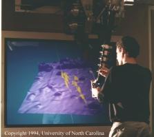
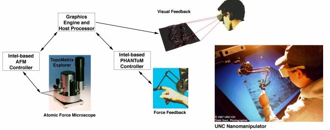
36 Nanomanipulators

37 Soft lithography, µ contact & µ molding

38 Soft lithography nano-imprint S. Chou, Princeton Mold Imprinted PMMA
39 Bottom-up methods
 nanosize structures Advantages Cheap")

40 Bottom-up Bottom-up methods start from molecules (atoms) to build up (functional) nanosize structures Advantages Cheap Dimensions ~10 nm Simple Low cost Disadvantages Low reproducibility No interconnection Successful examples Carbon nanotubes Quantum dots
41 Bottom-up
42 Bottom-up
43 Bottom-up Density of electronic states as a function of structure size.
44 Bottom-up


45 Bottom-up Perfect bottom-up example: cell division Self-assembly & self-replicating Cell replication needs thee classes of molecules: DNA RNA proteins


46 Molecular assembly 23 1mol s Molecular assembler Molecular gear, NASA Eric Drexler, Engine of Creation
47 Imagination is more important than knowledge. Albert Einstein
MSN551 LITHOGRAPHY II
 MSN551 Introduction to Micro and Nano Fabrication LITHOGRAPHY II E-Beam, Focused Ion Beam and Soft Lithography Why need electron beam lithography? Smaller features are required By electronics industry:
Nanotechnology Fabrication Methods.
 Nanotechnology Fabrication Methods. 10 / 05 / 2016 1 Summary: 1.Introduction to Nanotechnology:...3 2.Nanotechnology Fabrication Methods:...5 2.1.Top-down Methods:...7 2.2.Bottom-up Methods:...16 3.Conclusions:...19
Nanoimprint Lithography
 Nanoimprint Lithography Wei Wu Quantum Science Research Advanced Studies HP Labs, Hewlett-Packard Email: wei.wu@hp.com Outline Background Nanoimprint lithography Thermal based UV-based Applications based
Unconventional Nano-patterning. Peilin Chen
 Unconventional Nano-patterning Peilin Chen Reference Outlines History of patterning Traditional Nano-patterning Unconventional Nano-patterning Ancient Patterning "This is the Elks' land". A greeting at
Nanoelectronics 09. Atsufumi Hirohata Department of Electronics. Quick Review over the Last Lecture
 Nanoelectronics 09 Atsufumi Hirohata Department of Electronics 13:00 Monday, 12/February/2018 (P/T 006) Quick Review over the Last Lecture ( Field effect transistor (FET) ): ( Drain ) current increases
Chapter 12. Nanometrology. Oxford University Press All rights reserved.
 Chapter 12 Nanometrology Introduction Nanometrology is the science of measurement at the nanoscale level. Figure illustrates where nanoscale stands in relation to a meter and sub divisions of meter. Nanometrology
There s plenty of room at the bottom! - R.P. Feynman, Nanostructure: a piece of material with at least one dimension less than 100 nm in extent.
 Nanostructures and Nanotechnology There s plenty of room at the bottom! - R.P. Feynman, 1959 Materials behave differently when structured at the nm scale than they do in bulk. Technologies now exist that
Overview of the main nano-lithography techniques
 Overview of the main nano-lithography techniques Soraya Sangiao sangiao@unizar.es Outline Introduction: Nanotechnology. Nano-lithography techniques: Masked lithography techniques: Photolithography. X-ray
29: Nanotechnology. What is Nanotechnology? Properties Control and Understanding. Nanomaterials
 29: Nanotechnology What is Nanotechnology? Properties Control and Understanding Nanomaterials Making nanomaterials Seeing at the nanoscale Quantum Dots Carbon Nanotubes Biology at the Nanoscale Some Applications
There's Plenty of Room at the Bottom
 There's Plenty of Room at the Bottom 12/29/1959 Feynman asked why not put the entire Encyclopedia Britannica (24 volumes) on a pin head (requires atomic scale recording). He proposed to use electron microscope
Final Reading Assignment: Travels to the Nanoworld: pages pages pages
 Final Reading Assignment: Travels to the Nanoworld: pages 152-164 pages 201-214 pages 219-227 Bottom-up nanofabrication Can we assemble nanomachines manually? What are the components (parts)? nanoparticles
Nanotechnology. Gavin Lawes Department of Physics and Astronomy
 Nanotechnology Gavin Lawes Department of Physics and Astronomy Earth-Moon distance 4x10 8 m (courtesy NASA) Length scales (Part I) Person 2m Magnetic nanoparticle 5x10⁻⁹ m 10 10 m 10 5 m 1 m 10-5 m 10-10
Chapter 10. Nanometrology. Oxford University Press All rights reserved.
 Chapter 10 Nanometrology Oxford University Press 2013. All rights reserved. 1 Introduction Nanometrology is the science of measurement at the nanoscale level. Figure illustrates where nanoscale stands
Nanotechnology where size matters
 Nanotechnology where size matters J Emyr Macdonald Overview Ways of seeing very small things What is nanotechnology and why is it important? Building nanostructures What we can do with nanotechnology?
Chapter 1. Binary Systems 1-1. Outline. ! Introductions. ! Number Base Conversions. ! Binary Arithmetic. ! Binary Codes. ! Binary Elements 1-2
 Chapter 1 Binary Systems 1-1 Outline! Introductions! Number Base Conversions! Binary Arithmetic! Binary Codes! Binary Elements 1-2 3C Integration 傳輸與介面 IA Connecting 聲音與影像 Consumer Screen Phone Set Top
Scanning Tunneling Microscopy Transmission Electron Microscopy
 Scanning Tunneling Microscopy Transmission Electron Microscopy Speakers Burcu Başar Semih Gezgin Yavuz Selim Telis Place Hacettepe University Department of Chemical Engineering It s a small world after
Crystalline Surfaces for Laser Metrology
 Crystalline Surfaces for Laser Metrology A.V. Latyshev, Institute of Semiconductor Physics SB RAS, Novosibirsk, Russia Abstract: The number of methodological recommendations has been pronounced to describe
High-resolution Characterization of Organic Ultrathin Films Using Atomic Force Microscopy
 High-resolution Characterization of Organic Ultrathin Films Using Atomic Force Microscopy Jing-jiang Yu Nanotechnology Measurements Division Agilent Technologies, Inc. Atomic Force Microscopy High-Resolution
Nanostructured Materials - Fabrication Processes 1
 FABRICATION PROCESSES FOR NANOMATERIALS - NANOSTRUCTURES Lecture 6 1 Processes 1 SUBTRACTIVE AND MODIFYING METHODS Subtractive methods: Etching: wet chemical etching, reactive ion etching; ion beam sputter
Techniken der Oberflächenphysik (Techniques of Surface Physics)
") Techniken der Oberflächenphysik (Techniques of Surface Physics) Prof. Yong Lei & Dr. Yang Xu (& Liying Liang) Fachgebiet 3D-Nanostrukturierung, Institut für Physik Contact: yong.lei@tu-ilmenau.de; yang.xu@tu-ilmenau.de;
Techniken der Oberflächenphysik (Techniques of Surface Physics) Prof. Yong Lei & Dr. Yang Xu (& Liying Liang) Fachgebiet 3D-Nanostrukturierung, Institut für Physik Contact: yong.lei@tu-ilmenau.de; yang.xu@tu-ilmenau.de;
I. NANOFABRICATION O AND CHARACTERIZATION Chap. 2 : Self-Assembly
 I. Nanofabrication and Characterization : TOC I. NANOFABRICATION O AND CHARACTERIZATION Chap. 1 : Nanolithography Chap. 2 : Self-Assembly Chap. 3 : Scanning Probe Microscopy Nanoscale fabrication requirements
Kavli Workshop for Journalists. June 13th, CNF Cleanroom Activities
 Kavli Workshop for Journalists June 13th, 2007 CNF Cleanroom Activities Seeing nm-sized Objects with an SEM Lab experience: Scanning Electron Microscopy Equipment: Zeiss Supra 55VP Scanning electron microscopes
Transistor and Integrated Circuits: History
 Course Objective Review and practice fundamental chemical engineering concepts (mass, energy, and momentum transport coupled with heterogeneous and homogeneous reactions and thermodynamics). Apply these
From nanophysics research labs to cell phones. Dr. András Halbritter Department of Physics associate professor
 From nanophysics research labs to cell phones Dr. András Halbritter Department of Physics associate professor Curriculum Vitae Birth: 1976. High-school graduation: 1994. Master degree: 1999. PhD: 2003.
Nanostructures Fabrication Methods
 Nanostructures Fabrication Methods bottom-up methods ( atom by atom ) In the bottom-up approach, atoms, molecules and even nanoparticles themselves can be used as the building blocks for the creation of
Physicists in the Semiconductor Industry
 Physicists in the Semiconductor Industry P.M. Mooney IBM Research Division, T.J. Watson Research Center Yorktown Heights, NY 10598 APS March Meeting March 24, 2004 Thomas J. Watson Research Center 1 Outline
Techniken der Oberflächenphysik (Techniques of Surface Physics)
") Techniken der Oberflächenphysik (Techniques of Surface Physics) Prof. Yong Lei & Dr. Yang Xu Fachgebiet 3D-Nanostrukturierung, Institut für Physik Contact: yong.lei@tu-ilmenau.de yang.xu@tu-ilmenau.de
Techniken der Oberflächenphysik (Techniques of Surface Physics) Prof. Yong Lei & Dr. Yang Xu Fachgebiet 3D-Nanostrukturierung, Institut für Physik Contact: yong.lei@tu-ilmenau.de yang.xu@tu-ilmenau.de
RAJASTHAN TECHNICAL UNIVERSITY, KOTA
 RAJASTHAN TECHNICAL UNIVERSITY, KOTA (Electronics & Communication) Submitted By: LAKSHIKA SOMANI E&C II yr, IV sem. Session: 2007-08 Department of Electronics & Communication Geetanjali Institute of Technical
Lecture 14 Advanced Photolithography
 Lecture 14 Advanced Photolithography Chapter 14 Wolf and Tauber 1/74 Announcements Term Paper: You are expected to produce a 4-5 page term paper on a selected topic (from a list). Term paper contributes
Course file PPY15204 Nanoscience and Nanomaterials Table of Contents
 Department Physics Nanotechnology : M.sc Physics Course file PPY15204 Table Contents Second Year MSc Physics (2015-2016 Regulation) Detailed Lesson Plan UNIT-I: INTRODUCTION TO NANOTECHNOLOGY History Importance
Fabrication at the nanoscale for nanophotonics
 Fabrication at the nanoscale for nanophotonics Ilya Sychugov, KTH Materials Physics, Kista silicon nanocrystal by electron beam induced deposition lithography Outline of basic nanofabrication methods Devices
Nanolithography Techniques
 Nanolithography Techniques MSE 505 / MSNT 505 P. Coane Outline What Is Nanotechnology? The Motivation For Going Small Nanofabrication Technologies Basic Techniques Nano Lithography NANOTECHNOLOGY Nanotechnology
Moore s Law Forever?
 NCN Nanotechnology 101 Series Moore s Law Forever? Mark Lundstrom Purdue University Network for Computational Nanotechnology West Lafayette, IN USA NCN 1) Background 2) Transistors 3) CMOS 4) Beyond CMOS
Imaging Methods: Scanning Force Microscopy (SFM / AFM)
") Imaging Methods: Scanning Force Microscopy (SFM / AFM) The atomic force microscope (AFM) probes the surface of a sample with a sharp tip, a couple of microns long and often less than 100 Å in diameter.
Imaging Methods: Scanning Force Microscopy (SFM / AFM) The atomic force microscope (AFM) probes the surface of a sample with a sharp tip, a couple of microns long and often less than 100 Å in diameter.
Vapor-Phase Cutting of Carbon Nanotubes Using a Nanomanipulator Platform
 Vapor-Phase Cutting of Carbon Nanotubes Using a Nanomanipulator Platform MS&T 10, October 18, 2010 Vladimir Mancevski, President and CTO, Xidex Corporation Philip D. Rack, Professor, The University of
Nanomaterials and their Optical Applications
 Nanomaterials and their Optical Applications Winter Semester 2013 Lecture 02 rachel.grange@uni-jena.de http://www.iap.uni-jena.de/multiphoton Lecture 2: outline 2 Introduction to Nanophotonics Theoretical
CSCI 2570 Introduction to Nanocomputing
 CSCI 2570 Introduction to Nanocomputing The Emergence of Nanotechnology John E Savage Purpose of the Course The end of Moore s Law is in sight. Researchers are now exploring replacements for standard methods
Introduction. Photoresist : Type: Structure:
 Photoresist SEM images of the morphologies of meso structures and nanopatterns on (a) a positively nanopatterned silicon mold, and (b) a negatively nanopatterned silicon mold. Introduction Photoresist
Nanostructure. Materials Growth Characterization Fabrication. More see Waser, chapter 2
 Nanostructure Materials Growth Characterization Fabrication More see Waser, chapter 2 Materials growth - deposition deposition gas solid Physical Vapor Deposition Chemical Vapor Deposition Physical Vapor
MEEN Nanoscale Issues in Manufacturing. Lithography Lecture 1: The Lithographic Process
 MEEN 489-500 Nanoscale Issues in Manufacturing Lithography Lecture 1: The Lithographic Process 1 Discuss Reading Assignment 1 1 Introducing Nano 2 2 Size Matters 3 3 Interlude One-The Fundamental Science
Ecole Franco-Roumaine : Magnétisme des systèmes nanoscopiques et structures hybrides - Brasov, Modern Analytical Microscopic Tools
 1. Introduction Solid Surfaces Analysis Group, Institute of Physics, Chemnitz University of Technology, Germany 2. Limitations of Conventional Optical Microscopy 3. Electron Microscopies Transmission Electron
Nano-Lithography. Edited by Stefan Landis
 Nano-Lithography Edited by Stefan Landis IST^ m WILEY Table of Contents Foreword Jörge DE SOUSA NORONHA Introduction Michel BRILLOUET xi xvii Chapter 1. X-ray Lithography: Fundamentals and Applications
Copyright 2001 Scientific American, Inc.
 NANOFABRICATION art The of Building Small BY GEORGE M. WHITESIDES AND J. CHRISTOPHER LOVE RESEARCHERS ARE DISCOVERING CHEAP, EFFICIENT WAYS TO MAKE STRUCTURES ONLY A FEW BILLIONTHS OF A METER ACROSS INTRICATE
100 nm period gratings produced by lithographically induced self-construction
 INSTITUTE OFPHYSICS PUBLISHING Nanotechnology 14 (2003) 786 790 NANOTECHNOLOGY PII: S0957-4484(03)55891-3 100 nm period gratings produced by lithographically induced self-construction Xinya Lei, Lin Wu,
Like space travel and the Internet before it, the possibilities of the nano world catches the imagination of school children and scientists alike.
 The Nano World Preface Nano is the cool thing and it s the buzzword Like space travel and the Internet before it, the possibilities of the nano world catches the imagination of school children and scientists
Nano Materials. Nanomaterials
 Nano Materials 1 Contents Introduction Basics Synthesis of Nano Materials Fabrication of Nano Structure Nano Characterization Properties and Applications 2 Fabrication of Nano Structure Lithographic techniques
MSE 321 Structural Characterization
 Auger Spectroscopy Auger Electron Spectroscopy (AES) Scanning Auger Microscopy (SAM) Incident Electron Ejected Electron Auger Electron Initial State Intermediate State Final State Physical Electronics
MSE 321 Structural Characterization
 Auger Spectroscopy Auger Electron Spectroscopy (AES) Scanning Auger Microscopy (SAM) Incident Electron Ejected Electron Auger Electron Initial State Intermediate State Final State Physical Electronics
Technologies VII. Alternative Lithographic PROCEEDINGS OF SPIE. Douglas J. Resnick Christopher Bencher. Sponsored by. Cosponsored by.
 PROCEEDINGS OF SPIE Alternative Lithographic Technologies VII Douglas J. Resnick Christopher Bencher Editors 23-26 February 2015 San Jose, California, United States Sponsored by SPIE Cosponsored by DNS
0 volts. 2 volts. 5 volts
 CS101 Binary Storage Devices and Boolean Logic Now that we have discussed number representation, why do computers use the binary representation and not something we are more familiar with, like decimal?
CH676 Physical Chemistry: Principles and Applications. CH676 Physical Chemistry: Principles and Applications
 CH676 Physical Chemistry: Principles and Applications History of Nanotechnology: Time Line Democritus in ancient Greece: concept of atom 1900 : Rutherford : discovery of atomic nucleus The first TEM was
672 Advanced Solid State Physics. Scanning Tunneling Microscopy
 672 Advanced Solid State Physics Scanning Tunneling Microscopy Biao Hu Outline: 1. Introduction to STM 2. STM principle & working modes 3. STM application & extension 4. STM in our group 1. Introduction
Figure 1: Some examples of objects at different size scales ( 2001, CMP Científica, [2])
![Figure 1: Some examples of objects at different size scales ( 2001, CMP Científica, [2])](/thumbs/85/91872790.jpg "Figure 1: Some examples of objects at different size scales ( 2001, CMP Científica, [2])") Top-Down vs. Bottom-Up Nanomanufacturing Prof. Derek J. Hansford, Biomedical Engineering Program and Department of Materials Science & Engineering Learning Objectives: This module should expose the student
Top-Down vs. Bottom-Up Nanomanufacturing Prof. Derek J. Hansford, Biomedical Engineering Program and Department of Materials Science & Engineering Learning Objectives: This module should expose the student
Jeopardy Q $100 Q $100 Q $100 Q $100 Q $100 Q $200 Q $200 Q $200 Q $200 Q $200 Q $300 Q $300 Q $300 Q $300 Q $300 Q $400 Q $400 Q $400 Q $400 Q $400
 Jeopardy Size and Scale Nano Products Tools Structure Of Matter Science and Society Q $100 Q $200 Q $300 Q $400 Q $500 Q $100 Q $100 Q $100 Q $100 Q $200 Q $200 Q $200 Q $200 Q $300 Q $300 Q $300 Q $300
MICRO AND NANOPROCESSING TECHNOLOGIES
 LECTURE 5 MICRO AND NANOPROCESSING TECHNOLOGIES Introduction Ion lithography X-ray lithography Soft lithography E-beam lithography Concepts and processes Lithography systems Masks and resists Chapt.9.
Nova 600 NanoLab Dual beam Focused Ion Beam IITKanpur
 Nova 600 NanoLab Dual beam Focused Ion Beam system @ IITKanpur Dual Beam Nova 600 Nano Lab From FEI company (Dual Beam = SEM + FIB) SEM: The Electron Beam for SEM Field Emission Electron Gun Energy : 500
Südliche Stadtmauerstr. 15a Tel: D Erlangen Fax:
 Curriculum Vitae Lionel Santinacci 19.10.1974 Nationality: French Südliche Stadtmauerstr. 15a Tel: + 49 9131 852 7587 D-91054 Erlangen Fax: + 49 9131 852 7582 Germany e-mail: lionel@ww.uni-erlangen.de
1.0 Introduction. 1.1 Nanotechnology Historical Developments
 1.0 Introduction 1.1 Nanotechnology Historical Developments Around 370BC, Democritus a Greek philosopher developed the atomic theory of matter. Nano in GREEK means DWARF. The prefix nano means a billionth
Contents. What is AFM? History Basic principles and devices Operating modes Application areas Advantages and disadvantages
 Contents What is AFM? History Basic principles and devices Operating modes Application areas Advantages and disadvantages Figure1: 2004 Seth Copen Goldstein What is AFM? A type of Scanning Probe Microscopy
Direct-Write Deposition Utilizing a Focused Electron Beam
 Direct-Write Deposition Utilizing a Focused Electron Beam M. Fischer, J. Gottsbachner, S. Müller, W. Brezna, and H.D. Wanzenboeck Institute of Solid State Electronics, Vienna University of Technology,
Nanoscale Issues in Materials & Manufacturing
 Nanoscale Issues in Materials & Manufacturing ENGR 213 Principles of Materials Engineering Module 2: Introduction to Nanoscale Issues Top-down and Bottom-up Approaches for Fabrication Winfried Teizer,
Electrochemically Synthesized Multi-block
 Electrochemically Synthesized Multi-block Nanorods Sungho Park SungKyunKwan University, Department of Chemistry & SKKU Advanced Institute of Nanotechnology (SAINT) J. Am. Chem. Soc. 2003, 125, 2282-2290
Seminars in Nanosystems - I
 Seminars in Nanosystems - I Winter Semester 2011/2012 Dr. Emanuela Margapoti Emanuela.Margapoti@wsi.tum.de Dr. Gregor Koblmüller Gregor.Koblmueller@wsi.tum.de Seminar Room at ZNN 1 floor Topics of the
Introduction to Nanoscience and Nanotechnology
 Introduction to Nanoscience and Nanotechnology ENS 463 by Alexander M. Zaitsev alexander.zaitsev@csi.cuny.edu Tel: 718 982 2812 Office 4N101b 1 What is the size for a nano? 10-3 m, (milli) Macroobjects,
Sub-5 nm Patterning and Applications by Nanoimprint Lithography and Helium Ion Beam Lithography
 Sub-5 nm Patterning and Applications by Nanoimprint Lithography and Helium Ion Beam Lithography Yuanrui Li 1, Ahmed Abbas 1, Yuhan Yao 1, Yifei Wang 1, Wen-Di Li 2, Chongwu Zhou 1 and Wei Wu 1* 1 Department
Scanning Tunneling Microscopy
 Scanning Tunneling Microscopy Scanning Direction References: Classical Tunneling Quantum Mechanics Tunneling current Tunneling current I t I t (V/d)exp(-Aφ 1/2 d) A = 1.025 (ev) -1/2 Å -1 I t = 10 pa~10na
Nanotechnology. Yung Liou P601 Institute of Physics Academia Sinica
 Nanotechnology Yung Liou P601 yung@phys.sinica.edu.tw Institute of Physics Academia Sinica 1 1st week Definition of Nanotechnology The Interagency Subcommittee on Nanoscale Science, Engineering and Technology
Chapter 9. Electron mean free path Microscopy principles of SEM, TEM, LEEM
 Chapter 9 Electron mean free path Microscopy principles of SEM, TEM, LEEM 9.1 Electron Mean Free Path 9. Scanning Electron Microscopy (SEM) -SEM design; Secondary electron imaging; Backscattered electron
GRAPHENE ON THE Si-FACE OF SILICON CARBIDE USER MANUAL
 GRAPHENE ON THE Si-FACE OF SILICON CARBIDE USER MANUAL 1. INTRODUCTION Silicon Carbide (SiC) is a wide band gap semiconductor that exists in different polytypes. The substrate used for the fabrication
Probing Molecular Electronics with Scanning Probe Microscopy
 Probing Molecular Electronics with Scanning Probe Microscopy Mark C. Hersam Assistant Professor Department of Materials Science and Engineering, Northwestern University, Evanston, IL 60208-3108 Ph: 847-491-2696,
Single ion implantation for nanoelectronics and the application to biological systems. Iwao Ohdomari Waseda University Tokyo, Japan
 Single ion implantation for nanoelectronics and the application to biological systems Iwao Ohdomari Waseda University Tokyo, Japan Contents 1.History of single ion implantation (SII) 2.Novel applications
2008,, Jan 7 All-Paid US-Japan Winter School on New Functionalities in Glass. Controlling Light with Nonlinear Optical Glasses and Plasmonic Glasses
 2008,, Jan 7 All-Paid US-Japan Winter School on New Functionalities in Glass Photonic Glass Controlling Light with Nonlinear Optical Glasses and Plasmonic Glasses Takumi FUJIWARA Tohoku University Department
 http://www.physics.ucdavis.edu/condensed_matter.html A brief introduction to Condensed Matter Physics at Davis and an overview of the Condensed Matter Experiment Group The Past-- 30 Years of Nobel Prizes
NANOSCIENCE: TECHNOLOGY AND ADVANCED MATERIALS
 UNIVERSITY OF SOUTHAMPTON PHYS6014W1 SEMESTER 2 EXAMINATIONS 2012-2013 NANOSCIENCE: TECHNOLOGY AND ADVANCED MATERIALS DURATION 120 MINS (2 Hours) This paper contains 8 questions Answer ALL questions in
Dip-Pen Lithography 1
 Dip-Pen Lithography 1 A Brief History of Writing Instruments From Quills and Bamboos to fountain pens and brushes M. Klein and Henry W. Wynne received US patent #68445 in 1867 for an ink chamber and delivery
Photolithography 光刻 Part II: Photoresists
 微纳光电子材料与器件工艺原理 Photolithography 光刻 Part II: Photoresists Xing Sheng 盛兴 Department of Electronic Engineering Tsinghua University xingsheng@tsinghua.edu.cn 1 Photolithography 光刻胶 负胶 正胶 4 Photolithography
Electrical Characterization with SPM Application Modules
 Electrical Characterization with SPM Application Modules Metrology, Characterization, Failure Analysis: Data Storage Magnetoresistive (MR) read-write heads Semiconductor Transistors Interconnect Ferroelectric
materials, devices and systems through manipulation of matter at nanometer scale and exploitation of novel phenomena which arise because of the
 Nanotechnology is the creation of USEFUL/FUNCTIONAL materials, devices and systems through manipulation of matter at nanometer scale and exploitation of novel phenomena which arise because of the nanometer
Plasmonic and Diffractive Coupling in 2D Arrays of Nanoparticles Produced by Electron Beam Lithography
 Mater. Res. Soc. Symp. Proc. Vol. 951 2007 Materials Research Society 0951-E09-20 Plasmonic and Diffractive Coupling in 2D Arrays of Nanoparticles Produced by Electron Beam Lithography Erin McLellan 1,
ORION NanoFab: An Overview of Applications. White Paper
 ORION NanoFab: An Overview of Applications White Paper ORION NanoFab: An Overview of Applications Author: Dr. Bipin Singh Carl Zeiss NTS, LLC, USA Date: September 2012 Introduction With the advancement
Introduction to Scanning Probe Microscopy Zhe Fei
 Introduction to Scanning Probe Microscopy Zhe Fei Phys 590B, Apr. 2019 1 Outline Part 1 SPM Overview Part 2 Scanning tunneling microscopy Part 3 Atomic force microscopy Part 4 Electric & Magnetic force
Special Topics in Semiconductor Nanotechnology ECE 598XL
 Special Topics in Semiconductor Nanotechnology ECE 598XL Fall 2009 ECE 598XL Syllabus Overview: size matters Formation Process Characterization SOA device applications and potentials Homework or quizzes
Carbon Nanotube Thin-Films & Nanoparticle Assembly
 Nanodevices using Nanomaterials : Carbon Nanotube Thin-Films & Nanoparticle Assembly Seung-Beck Lee Division of Electronics and Computer Engineering & Department of Nanotechnology, Hanyang University,
MeV electron diffraction and microscopy
 UESDM, UCLA, Dec. 12 14, 2012 MeV electron diffraction and microscopy in Osaka University Jinfeng Yang Osaka University, Japan Collaborators: (RIKEN) Yoshie Murooka (Osaka Univ.) Y. Naruse, K. Kan, K.
Scanning Tunneling Microscopy
 Scanning Tunneling Microscopy References: 1. G. Binnig, H. Rohrer, C. Gerber, and Weibel, Phys. Rev. Lett. 49, 57 (1982); and ibid 50, 120 (1983). 2. J. Chen, Introduction to Scanning Tunneling Microscopy,
PHYS 3313 Section 001 Lecture #21 Monday, Nov. 26, 2012
 PHYS 3313 Section 001 Lecture #21 Monday, Nov. 26, 2012 Superconductivity Theory, The Cooper Pair Application of Superconductivity Semi-Conductor Nano-technology Graphene 1 Announcements Your presentations
CURRENT STATUS OF NANOIMPRINT LITHOGRAPHY DEVELOPMENT IN CNMM
 U.S. -KOREA Forums on Nanotechnology 1 CURRENT STATUS OF NANOIMPRINT LITHOGRAPHY DEVELOPMENT IN CNMM February 17 th 2005 Eung-Sug Lee,Jun-Ho Jeong Korea Institute of Machinery & Materials U.S. -KOREA Forums
Presentation Phys Katia GASPERI. Statistical study of single DNA molecules into dynamic array
 Presentation Phys 730 - Katia GASPERI Statistical study of single DNA molecules into dynamic array 1 Statistical study of single DNA molecules into dynamic array - Research project lead by Laurence SALOME
Current and Emergent Developments
 Self Assembly and Biologically Inspired Processes in Applied Nanotechnology: Current and Emergent Developments Charles Ostman VP, Electronics & Photonics Forum chair NanoSig Senior Consultant Silicon Valley
Fabrication of ordered array at a nanoscopic level: context
 Fabrication of ordered array at a nanoscopic level: context Top-down method Bottom-up method Classical lithography techniques Fast processes Size limitations it ti E-beam techniques Small sizes Slow processes
Electronic Supplementary Information
 Electronic Supplementary Information High Electrocatalytic Activity of Self-standing Hollow NiCo 2 S 4 Single Crystalline Nanorod Arrays towards Sulfide Redox Shuttles in Quantum Dot-sensitized Solar Cells
Spectroscopy at nanometer scale
 Spectroscopy at nanometer scale 1. Physics of the spectroscopies 2. Spectroscopies for the bulk materials 3. Experimental setups for the spectroscopies 4. Physics and Chemistry of nanomaterials Various
Presentation Phys Katia GASPERI. Statistical study of single DNA molecules into dynamic array
 Presentation Phys 730 - Katia GASPERI Statistical study of single DNA molecules into dynamic array 1 Statistical study of single DNA molecules into dynamic array - Research project lead by Laurence SALOME
LECTURE 1 : INTRODUCTION TO NANOMECHANICS
 I LECTURE 1 : INTRODUCTION TO NANOMECHANICS Outline : NANOTECHNOLOGY / NANOMECHANICS DEFINITIONS... 2 WHY IS NANO INTERESTING?... 3 HISTORY OF NANOTECHNOLOGY/NANOMECHANICS : TIME LINE... 4 The First Talk
SYLLABUS FINDING NANO Syllabus NanoSCI DISCOVERING NANOTECHNOLOGY AND CULTURE IN GERMANY
 1. Syllabus NanoSCI Course title: NanoSCI - Electronic Properties of Nanoengineered Materials Catalog description: Physics and technology of nanoengineered materials and devices. Semiconductor nanostructures.
Lesson 4: Tools of the Nanosciences. Student Materials
 Lesson 4: Tools of the Nanosciences Student Materials Contents Black Box Lab Activity: Student Instructions and Worksheet Seeing and Building Small Things: Student Reading Seeing and Building Small Things:
Cross Section and Line Edge Roughness Metrology for EUV Lithography using Critical Dimension Small Angle X-ray X
 Cross Section and Line Edge Roughness Metrology for EUV Lithography using Critical Dimension Small Angle X-ray X Scattering Ronald L. Jones, Wen-li Wu, Eric K. Lin NIST Polymers Division, Gaithersburg,
Photoacoustic metrology of nanoimprint polymers
 Photoacoustic metrology of nanoimprint polymers T. Kehoe a, J. Bryner b, J. Vollmann b, C. Sotomayor Torres a, L. Aebi b and J. Dual b a Tyndall National Institute, Lee Maltings, University College Cork,
Fabrication and Domain Imaging of Iron Magnetic Nanowire Arrays
 Abstract #: 983 Program # MI+NS+TuA9 Fabrication and Domain Imaging of Iron Magnetic Nanowire Arrays D. A. Tulchinsky, M. H. Kelley, J. J. McClelland, R. Gupta, R. J. Celotta National Institute of Standards
Large scale growth and characterization of atomic hexagonal boron. nitride layers
 Supporting on-line material Large scale growth and characterization of atomic hexagonal boron nitride layers Li Song, Lijie Ci, Hao Lu, Pavel B. Sorokin, Chuanhong Jin, Jie Ni, Alexander G. Kvashnin, Dmitry