EV Group. Engineered Substrates for future compound semiconductor devices
|
|
|
- Phillip Dean
- 5 years ago
- Views:
Transcription

1 EV Group Engineered Substrates for future compound semiconductor devices

 SOS (Silicon on Sapphire) SOI (Silicon on Insulator) Heterogeneous")


2 Engineered Substrates HB-LED: Engineered growth substrates GaN / GaP layer transfer Mobility enhancement solutions: III-Vs to silicon (e.g. GaAs, GaP, InP, GaN) GOI (Germanium on Insulator) ssoi (strained silicon on insulator) SOS (Silicon on Sapphire) SOI (Silicon on Insulator) Heterogeneous integration: Optical solutions on silicon MEMS on silicon Thermal management: Silicon on Silicon Carbide Silicon on Diamond Multi-Junction solar cells Courtesy of OSRAM OS Courtesy of Soitec Courtesy of J. Bowers UCSB Novel applications such as graphene, spintronics, Courtesy of RIT Courtesy of D. Awschalom UCSB EV Group Semicon Europa
3 Integration of Compound Semiconductors Hetero- Epitaxy CS growth on dissimilar substrates (e.g Si) Dissimilar crystal and physical parameters High dislocation densities of the grown films Wafer bonding Layer transfer from growth wafers to a functional substrate Hybrid Integration Integration of multiple CS materials by epitaxial growth & layer transfer EV Group Semicon Europa
4 Integration of Compound Semiconductors cont d Problem Different states in manufacturing and operation demand different substrates properties: Structural properties (lattice matching, thermal expansion, etc.) Electrical properties Mechanical properties Engineered Substrates Creating a substrate with unique, combined properties as desired for the further processing Joining materials of different properties Altering the material properties by pre-treatment EV Group Semicon Europa


5 Outline EV Group Semicon Europa

6 Outline Direct wafer bonding for compound semiconductor layer transfer and growth substrate manufacturing Temporary bonding for thin wafer/film handling of compound semiconductors EV Group Semicon Europa

7 HB-LEDs GaN on sapphire or silicon Problem Hetero epitaxy of GaN on sapphire or silicon results in a high density of threading dislocations, due to: Lattice mismatch CTE mismatch Solutions Patterned sapphire substrates Pendeo epitaxy / ELOG Chung et al. Appl.Phys.Lett. 95 (2009) EV Group Semicon Europa


8 Patterned Sapphire Substrates (PSS) Improved GaN quality with higher efficiency Increased light extraction efficiency Faster etching with smaller PSS features Faster coalescence for following epitaxial growth step Clear Clear trend trend is is visible visible to to move move from from micron-sized features to to sub-micron features Adapted H. Kuo, NCTU EV Group Semicon Europa
9 Pendeo-Epitaxy / Epitaxial Layer Overgrowth Hard mask GaN seed layer GaN etching Substrate (SiC, Si, etc) GaN overgrowth AlGaN overgrowth K.J. Gehrke et al, MRS Internet J. Semicond. Res. (1999) 4S1, G3.2 EV Group Semicon Europa
 (NIL) enables the")


10 UV NIL Process flow Nanoimprint Lithography (NIL) (NIL) enables the the cost-efficient, large large area area generation of of micro- micro-and nanometer scale scale growth growth structures. EV Group Semicon Europa


11 UV NIL Process flow UV - Nanoimprint Lithography (UV-NIL, UV Molding) Benefits of UV-NIL with soft stamps: - Micro- and nano-features in one imprint - Achieved Resolution: < 15nm - Low CoO with soft stamp technology - 3D structures Master provided by NILT


12 From R&D to HVM Equipment Portfolio HVM UV-NIL THERMAL NIL R&D
13 Photon management θ in > θ crit θ in > θ crit n 1 n 2 n 1 n 2 HB-LEDs Light extraction features like PhCs on the LED surface results in: Higher extraction efficiency Extraction of lower order modes Direction of extracted light (quasi periodic PhCs) Photovoltaics Texturization increases the cell efficiency due to: Reduced reflectivity Deflection of incoming light resulting in light trapping Nanoimprint Lithography (NIL) (NIL) enables innovative surface surface textures for for photon photon management.
14 Outline Nanoimprint lithography (NIL) for growth enhancement structures Direct wafer bonding for compound semiconductor layer transfer and growth substrate manufacturing Temporary bonding for thin wafer/film handling of compound semiconductors


15 Overview Wafer Bonding Processes


 - Engi")
16 Ex situ process flow Mechanical alignment accuracy ~50µm Optical alignment accuracy ~1µm Applications - Substrates manufacturing (SOI, GOI, SSOI, etc.) - Engineered substrates - MEMS (e.g. 3D assembly, packaging, capping) - 3D interconnects


 Cross")

17 SOI by Wafer Bonding Bonding interface Bonded SOI wafers (SOITEC - FRANCE) Cross section TEM image of a bonded SOI substrate.
 Plasma-activated fusion bonding TEM cross section of InGaAs channel bonded to a silicon carrier Takagi et al.")
18 High mobility logic application InGaAs carries high potential for the n-mos transistor in future CMOS High mobility requirements are closely tied to the structural material properties Low annealing budget after bonding (InGaAs damage) Plasma-activated fusion bonding TEM cross section of InGaAs channel bonded to a silicon carrier Takagi et al. VLSI Summit 2010
 on silicon Plasma activation for low temperature bonding (SOI wafer manufacturing and InP to silicon bonding) Liang et al.")
19 InP-based Si photonics Challenge: Silicon s indirect band-gap results in emission of phonons (heat) Photon generation internal quantum efficiency is as low as 1:10 6 Room-temperature applications demand the integration of III-Vs with silicon Solution: Wafer bonding of III-Vs (e.g. InP) on silicon Plasma activation for low temperature bonding (SOI wafer manufacturing and InP to silicon bonding) Liang et al. Nature Photonics 4 (2010) 511 Bowers, Optics & Photonics News, May 2010, p.28

20 Engineered Growth Substrates GaN and sapphire feature around 16% lattice mismatch (RT) Sapphire prices expected to increase by ~40% in 2011 Courtesy of Soitec Highly lattice & CTE matched substrates for epitaxial growth of GaN with low defect density Increased throughput Higher internal quantum efficiency Improved yield and lower binning Courtesy of J. Bowers / UCSB

21 Outline Nanoimprint lithography (NIL) for growth enhancement structures Direct wafer bonding for compound semiconductor layer transfer and growth substrate manufacturing

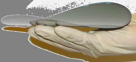

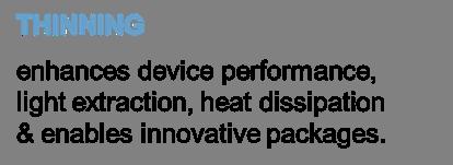
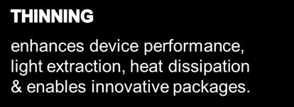
22 Thin wafer processing Thinning


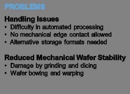
23 Thin wafer processing Temporary bonding and debonding Enables utilization of existing equipment and existing processes (Back thinning, TSV formation, backside metallization, etc..)
24 Conclusion Engineered substrates are gaining importance with the increasing market size of compound semiconductor devices. Different technologies for the creation of engineered substrates have been introduced: Nanoimprint Lithography Wafer bonding Temporary bonding Engineered substrates will play an important role for the implementation of compound semiconductors on silicon. Monolithic device layouts Higher integration and miniaturization Engineered growth substrates for HB-LEDs offer a high potential for increasing efficiency, higher crystal quality and reduced binning.
25 EV Group
Self-study problems and questions Processing and Device Technology, FFF110/FYSD13
 Self-study problems and questions Processing and Device Technology, FFF110/FYSD13 Version 2016_01 In addition to the problems discussed at the seminars and at the lectures, you can use this set of problems
EV Group. Enabling processes for 3D interposer. Dr. Thorsten Matthias EV Group
 EV Group Enabling processes for 3D interposer Dr. Thorsten Matthias EV Group EV Group in a Nutshell st Our philosophy Our mission in serving next generation application in semiconductor technology Equipment
Currently, worldwide major semiconductor alloy epitaxial growth is divided into two material groups.
 ICQNM 2014 Currently, worldwide major semiconductor alloy epitaxial growth is divided into two material groups. Cubic: Diamond structures: group IV semiconductors (Si, Ge, C), Cubic zinc-blende structures:
2D MBE Activities in Sheffield. I. Farrer, J. Heffernan Electronic and Electrical Engineering The University of Sheffield
 2D MBE Activities in Sheffield I. Farrer, J. Heffernan Electronic and Electrical Engineering The University of Sheffield Outline Motivation Van der Waals crystals The Transition Metal Di-Chalcogenides
Photodetector. Prof. Woo-Young Choi. Silicon Photonics (2012/2) Photodetection: Absorption => Current Generation. Currents
 Photodetection: Absorption => Current Generation. Currents") Photodetection: Absorption => Current Generation h Currents Materials for photodetection: E g < h Various methods for generating currents with photo-generated carriers: photoconductors, photodiodes, avalanche
Photodetection: Absorption => Current Generation h Currents Materials for photodetection: E g < h Various methods for generating currents with photo-generated carriers: photoconductors, photodiodes, avalanche
EE130: Integrated Circuit Devices
 EE130: Integrated Circuit Devices (online at http://webcast.berkeley.edu) Instructor: Prof. Tsu-Jae King (tking@eecs.berkeley.edu) TA s: Marie Eyoum (meyoum@eecs.berkeley.edu) Alvaro Padilla (apadilla@eecs.berkeley.edu)
LATEST INSIGHTS IN MATERIAL AND PROCESS TECHNOLOGIES FOR INTERPOSER AND 3D STACKING
 LATEST INSIGHTS IN MATERIAL AND PROCESS TECHNOLOGIES FOR INTERPOSER AND 3D STACKING European 3D TSV Summit, January 22-23, 2013, Grenoble Dr. Rainer Knippelmeyer, CTO and VP of R&D, GM Product Line Bonder
Graphene films on silicon carbide (SiC) wafers supplied by Nitride Crystals, Inc.
 wafers supplied by Nitride Crystals, Inc.") 9702 Gayton Road, Suite 320, Richmond, VA 23238, USA Phone: +1 (804) 709-6696 info@nitride-crystals.com www.nitride-crystals.com Graphene films on silicon carbide (SiC) wafers supplied by Nitride Crystals,
9702 Gayton Road, Suite 320, Richmond, VA 23238, USA Phone: +1 (804) 709-6696 info@nitride-crystals.com www.nitride-crystals.com Graphene films on silicon carbide (SiC) wafers supplied by Nitride Crystals,
Lecture 0: Introduction
 Lecture 0: Introduction Introduction q Integrated circuits: many transistors on one chip q Very Large Scale Integration (VLSI): bucketloads! q Complementary Metal Oxide Semiconductor Fast, cheap, low power
CURRENT STATUS OF NANOIMPRINT LITHOGRAPHY DEVELOPMENT IN CNMM
 U.S. -KOREA Forums on Nanotechnology 1 CURRENT STATUS OF NANOIMPRINT LITHOGRAPHY DEVELOPMENT IN CNMM February 17 th 2005 Eung-Sug Lee,Jun-Ho Jeong Korea Institute of Machinery & Materials U.S. -KOREA Forums
Fundamentals of Nanoelectronics: Basic Concepts
 Fundamentals of Nanoelectronics: Basic Concepts Sławomir Prucnal FWIM Page 1 Introduction Outline Electronics in nanoscale Transport Ohms law Optoelectronic properties of semiconductors Optics in nanoscale
Three-Dimensional Silicon-Germanium Nanostructures for Light Emitters and On-Chip Optical. Interconnects
 Three-Dimensional Silicon-Germanium Nanostructures for Light Emitters and On-Chip Optical eptember 2011 Interconnects Leonid Tsybeskov Department of Electrical and Computer Engineering New Jersey Institute
III-V nanostructured materials synthesized by MBE droplet epitaxy
 III-V nanostructured materials synthesized by MBE droplet epitaxy E.A. Anyebe 1, C. C. Yu 1, Q. Zhuang 1,*, B. Robinson 1, O Kolosov 1, V. Fal ko 1, R. Young 1, M Hayne 1, A. Sanchez 2, D. Hynes 2, and
SHRINK. STACK. INTEGRATE.
 SHRINK. STACK. INTEGRATE. SUSS MICROTEC PRODUCT PORTFOLIO SHAPING THE FUTURE With more than 60 years of engineering experience SUSS MicroTec is a leading supplier of process equipment for microstructuring
IBM T.J. Watson Research Center
 IBM T.J. Watson Research Center 2D material based layer transfer Jeehwan Kim Prof. of Mechanical Engineering Prof. of Materials science and Engineering Jeehwan Kim Research Group http://jeehwanlab.mit.edu
Semiconductor Physics and Devices
 Syllabus Advanced Nano Materials Semiconductor Physics and Devices Textbook Donald A. Neamen (McGraw-Hill) Semiconductor Physics and Devices Seong Jun Kang Department of Advanced Materials Engineering
Exceptional ballistic transport in epigraphene. Walt de Heer Georgia Institute of Technology
 Exceptional ballistic transport in epigraphene Walt de Heer Georgia Institute of Technology Program Objective First formulated in 2001 and patented in 2003, our objective is to develop nanoelectronics
Thin Wafer Handling Challenges and Emerging Solutions
 1 Thin Wafer Handling Challenges and Emerging Solutions Dr. Shari Farrens, Mr. Pete Bisson, Mr. Sumant Sood and Mr. James Hermanowski SUSS MicroTec, 228 Suss Drive, Waterbury Center, VT 05655, USA 2 Thin
Fabrication Technology, Part I
 EEL5225: Principles of MEMS Transducers (Fall 2004) Fabrication Technology, Part I Agenda: Microfabrication Overview Basic semiconductor devices Materials Key processes Oxidation Thin-film Deposition Reading:
Passionately Innovating With Customers To Create A Connected World
 Passionately Innovating With Customers To Create A Connected World Multi Die Integration Can Material Suppliers Meet the Challenge? Nov 14, 2012 Jeff Calvert - R&D Director, Advanced Packaging Technologies
Plan for Lectures #4, 5, & 6. Theme Of Lectures: Nano-Fabrication
 Plan for Lectures #4, 5, & 6 Theme Of Lectures: Nano-Fabrication Quantum Wells, SLs, Epitaxial Quantum Dots Carbon Nanotubes, Semiconductor Nanowires Self-assembly and Self-organization Two Approaches
TCAD Modeling of Stress Impact on Performance and Reliability
 TCAD Modeling of Stress Impact on Performance and Reliability Xiaopeng Xu TCAD R&D, Synopsys March 16, 2010 SEMATECH Workshop on Stress Management for 3D ICs using Through Silicon Vias 1 Outline Introduction
Lecture 2. Semiconductor Physics. Sunday 4/10/2015 Semiconductor Physics 1-1
 Lecture 2 Semiconductor Physics Sunday 4/10/2015 Semiconductor Physics 1-1 Outline Intrinsic bond model: electrons and holes Charge carrier generation and recombination Intrinsic semiconductor Doping:
Chemistry Instrumental Analysis Lecture 8. Chem 4631
 Chemistry 4631 Instrumental Analysis Lecture 8 UV to IR Components of Optical Basic components of spectroscopic instruments: stable source of radiant energy transparent container to hold sample device
Hybrid Wafer Level Bonding for 3D IC
 Hybrid Wafer Level Bonding for 3D IC An Equipment Perspective Markus Wimplinger, Corporate Technology Development & IP Director History & Roadmap - BSI CIS Devices???? 2013 2 nd Generation 3D BSI CIS with
Thin Wafer Handling Debonding Mechanisms
 Thin Wafer Handling Debonding Mechanisms Jonathan Jeauneau, Applications Manager Alvin Lee, Technology Strategist Dongshun Bai, Scientist, 3-D IC R&D Materials Outline Requirements of Thin Wafer Handling
Band Gap Engineering. Reading the Periodic Table and Understanding Optical and Electrical Properties in Semiconductors
 The Birnie Group solar class and website were created with much-appreciated support from the NSF CRCD Program under grants 0203504 and 0509886. Continuing Support from the McLaren Endowment is also greatly
Normally-Off GaN Field Effect Power Transistors: Device Design and Process Technology Development
 Center for High Performance Power Electronics Normally-Off GaN Field Effect Power Transistors: Device Design and Process Technology Development Dr. Wu Lu (614-292-3462, lu.173@osu.edu) Dr. Siddharth Rajan
Chapter 3 Basics Semiconductor Devices and Processing
 Chapter 3 Basics Semiconductor Devices and Processing Hong Xiao, Ph. D. www2.austin.cc.tx.us/hongxiao/book.htm Hong Xiao, Ph. D. www2.austin.cc.tx.us/hongxiao/book.htm 1 Objectives Identify at least two
ELECTRONIC DEVICES AND CIRCUITS SUMMARY
 ELECTRONIC DEVICES AND CIRCUITS SUMMARY Classification of Materials: Insulator: An insulator is a material that offers a very low level (or negligible) of conductivity when voltage is applied. Eg: Paper,
Lecture 8. Detectors for Ionizing Particles
 Lecture 8 Detectors for Ionizing Particles Content Introduction Overview of detector systems Sources of radiation Radioactive decay Cosmic Radiation Accelerators Interaction of Radiation with Matter General
Chapter 1 Overview of Semiconductor Materials and Physics
 Chapter 1 Overview of Semiconductor Materials and Physics Professor Paul K. Chu Conductivity / Resistivity of Insulators, Semiconductors, and Conductors Semiconductor Elements Period II III IV V VI 2 B
MSN551 LITHOGRAPHY II
 MSN551 Introduction to Micro and Nano Fabrication LITHOGRAPHY II E-Beam, Focused Ion Beam and Soft Lithography Why need electron beam lithography? Smaller features are required By electronics industry:
3.1 Introduction to Semiconductors. Y. Baghzouz ECE Department UNLV
 3.1 Introduction to Semiconductors Y. Baghzouz ECE Department UNLV Introduction In this lecture, we will cover the basic aspects of semiconductor materials, and the physical mechanisms which are at the
ET3034TUx Utilization of band gap energy
 ET3034TUx - 3.3.1 - Utilization of band gap energy In the last two weeks we have discussed the working principle of a solar cell and the external parameters that define the performance of a solar cell.
Lecture 1. Introduction to Electronic Materials. Reading: Pierret 1.1, 1.2, 1.4,
 Lecture 1 Introduction to Electronic Materials Reading: Pierret 1.1, 1.2, 1.4, 2.1-2.6 Atoms to Operational Amplifiers The goal of this course is to teach the fundamentals of non-linear circuit elements
Electron Energy, E E = 0. Free electron. 3s Band 2p Band Overlapping energy bands. 3p 3s 2p 2s. 2s Band. Electrons. 1s ATOM SOLID.
 Electron Energy, E Free electron Vacuum level 3p 3s 2p 2s 2s Band 3s Band 2p Band Overlapping energy bands Electrons E = 0 1s ATOM 1s SOLID In a metal the various energy bands overlap to give a single
Chapter 2. Design and Fabrication of VLSI Devices
 Chapter 2 Design and Fabrication of VLSI Devices Jason Cong 1 Design and Fabrication of VLSI Devices Objectives: To study the materials used in fabrication of VLSI devices. To study the structure of devices
A semiconductor is an almost insulating material, in which by contamination (doping) positive or negative charge carriers can be introduced.
 positive or negative charge carriers can be introduced.") Semiconductor A semiconductor is an almost insulating material, in which by contamination (doping) positive or negative charge carriers can be introduced. Page 2 Semiconductor materials Page 3 Energy levels
Semiconductor A semiconductor is an almost insulating material, in which by contamination (doping) positive or negative charge carriers can be introduced. Page 2 Semiconductor materials Page 3 Energy levels
GRAPHENE ON THE Si-FACE OF SILICON CARBIDE USER MANUAL
 GRAPHENE ON THE Si-FACE OF SILICON CARBIDE USER MANUAL 1. INTRODUCTION Silicon Carbide (SiC) is a wide band gap semiconductor that exists in different polytypes. The substrate used for the fabrication
EECS143 Microfabrication Technology
 EECS143 Microfabrication Technology Professor Ali Javey Introduction to Materials Lecture 1 Evolution of Devices Yesterday s Transistor (1947) Today s Transistor (2006) Why Semiconductors? Conductors e.g
Recent progress in MOCVD Technology for Electronic and Optoelectronic Devices
 AIXTRON SE Recent progress in MOCVD Technology for Electronic and Optoelectronic Devices Prof Dr.-Ing. Michael Heuken 1,2 Vice President Corporate Research&Development 1) AIXTRON SE, Dornkaulstr. 2, 52134
Technologies VII. Alternative Lithographic PROCEEDINGS OF SPIE. Douglas J. Resnick Christopher Bencher. Sponsored by. Cosponsored by.
 PROCEEDINGS OF SPIE Alternative Lithographic Technologies VII Douglas J. Resnick Christopher Bencher Editors 23-26 February 2015 San Jose, California, United States Sponsored by SPIE Cosponsored by DNS
Crystal Properties. MS415 Lec. 2. High performance, high current. ZnO. GaN
 Crystal Properties Crystal Lattices: Periodic arrangement of atoms Repeated unit cells (solid-state) Stuffing atoms into unit cells Determine mechanical & electrical properties High performance, high current
Physics of Semiconductors
 Physics of Semiconductors 9 th 2016.6.13 Shingo Katsumoto Department of Physics and Institute for Solid State Physics University of Tokyo Site for uploading answer sheet Outline today Answer to the question
Ge Quantum Well Modulators on Si. D. A. B. Miller, R. K. Schaevitz, J. E. Roth, Shen Ren, and Onur Fidaner
 10.1149/1.2986844 The Electrochemical Society Ge Quantum Well Modulators on Si D. A. B. Miller, R. K. Schaevitz, J. E. Roth, Shen Ren, and Onur Fidaner Ginzton Laboratory, 450 Via Palou, Stanford CA 94305-4088,
PHOTOVOLTAICS Fundamentals
 PHOTOVOLTAICS Fundamentals PV FUNDAMENTALS Semiconductor basics pn junction Solar cell operation Design of silicon solar cell SEMICONDUCTOR BASICS Allowed energy bands Valence and conduction band Fermi
Conductivity and Semi-Conductors
 Conductivity and Semi-Conductors J = current density = I/A E = Electric field intensity = V/l where l is the distance between two points Metals: Semiconductors: Many Polymers and Glasses 1 Electrical Conduction
UNIVERSITY OF CALIFORNIA College of Engineering Department of Electrical Engineering and Computer Sciences. Fall Exam 1
 UNIVERSITY OF CALIFORNIA College of Engineering Department of Electrical Engineering and Computer Sciences EECS 143 Fall 2008 Exam 1 Professor Ali Javey Answer Key Name: SID: 1337 Closed book. One sheet
ALIGNMENT ACCURACY IN A MA/BA8 GEN3 USING SUBSTRATE CONFORMAL IMPRINT LITHOGRAPHY (SCIL)
") ALIGNMENT ACCURACY IN A MA/BA8 GEN3 USING SUBSTRATE CONFORMAL IMPRINT LITHOGRAPHY (SCIL) Robert Fader Fraunhofer Institute for Integrated Systems and Device Technology (IISB) Germany Ulrike Schömbs SUSS
ALIGNMENT ACCURACY IN A MA/BA8 GEN3 USING SUBSTRATE CONFORMAL IMPRINT LITHOGRAPHY (SCIL) Robert Fader Fraunhofer Institute for Integrated Systems and Device Technology (IISB) Germany Ulrike Schömbs SUSS
EE143 Fall 2016 Microfabrication Technologies. Evolution of Devices
 EE143 Fall 2016 Microfabrication Technologies Prof. Ming C. Wu wu@eecs.berkeley.edu 511 Sutardja Dai Hall (SDH) 1-1 Evolution of Devices Yesterday s Transistor (1947) Today s Transistor (2006) 1-2 1 Why
Practical Quantum-Dot Lasers Monolithically Grown on Silicon for Silicon Photonics
 Department of Electronic and Electrical Engineering London Centre for Nanotechnology Practical Quantum-Dot Lasers Monolithically Grown on Silicon for Silicon Photonics Huiyun Liu Outline Why lasers on
Part 5: Quantum Effects in MOS Devices
 Quantum Effects Lead to Phenomena such as: Ultra Thin Oxides Observe: High Leakage Currents Through the Oxide - Tunneling Depletion in Poly-Si metal gate capacitance effect Thickness of Inversion Layer
CHAPTER 11 Semiconductor Theory and Devices
 CHAPTER 11 Semiconductor Theory and Devices 11.1 Band Theory of Solids 11.2 Semiconductor Theory 11.3 Semiconductor Devices 11.4 Nanotechnology It is evident that many years of research by a great many
Semi-insulating SiC substrates for high frequency devices
 Klausurtagung Silberbach, 19. - 21. Feb. 2002 Institut für Werkstoffwissenschaften - WW 6 Semi-insulating SiC substrates for high frequency devices Vortrag von Matthias Bickermann Semi-insulating SiC substrates
Halbleiter. Prof. Yong Lei. Prof. Thomas Hannappel.
 Halbleiter Prof. Yong Lei Prof. Thomas Hannappel yong.lei@tu-ilemnau.de thomas.hannappel@tu-ilmenau.de Important Events in Semiconductors History 1833 Michael Faraday discovered temperature-dependent conductivity
GaN for use in harsh radiation environments
 4 th RD50 - Workshop on radiation hard semiconductor devices for very high luminosity colliders GaN for use in harsh radiation environments a (W Cunningham a, J Grant a, M Rahman a, E Gaubas b, J Vaitkus
Ion Implant Part 1. Saroj Kumar Patra, TFE4180 Semiconductor Manufacturing Technology. Norwegian University of Science and Technology ( NTNU )
") 1 Ion Implant Part 1 Chapter 17: Semiconductor Manufacturing Technology by M. Quirk & J. Serda Spring Semester 2014 Saroj Kumar Patra,, Norwegian University of Science and Technology ( NTNU ) 2 Objectives
1 Ion Implant Part 1 Chapter 17: Semiconductor Manufacturing Technology by M. Quirk & J. Serda Spring Semester 2014 Saroj Kumar Patra,, Norwegian University of Science and Technology ( NTNU ) 2 Objectives
Classification of Solids
 Classification of Solids Classification by conductivity, which is related to the band structure: (Filled bands are shown dark; D(E) = Density of states) Class Electron Density Density of States D(E) Examples
Reliability of 3D IC with Via-Middle TSV: Characterization and Modeling
 Reliability of 3D IC with Via-Middle TSV: Characterization and Modeling Victor Moroz *, Munkang Choi *, Geert Van der Plas, Paul Marchal, Kristof Croes, and Eric Beyne * Motivation: Build Reliable 3D IC
Semiconductor Device Physics
 1 Semiconductor Device Physics Lecture 1 http://zitompul.wordpress.com 2 0 1 3 2 Semiconductor Device Physics Textbook: Semiconductor Device Fundamentals, Robert F. Pierret, International Edition, Addison
Basic cell design. Si cell
 Basic cell design Si cell 1 Concepts needed to describe photovoltaic device 1. energy bands in semiconductors: from bonds to bands 2. free carriers: holes and electrons, doping 3. electron and hole current:
SPCC Department of Bio-Nano Technology and 2 Materials Science and Chemical Engineering, Hanyang University, Ansan, 15588, Republic of Korea.
 SPCC 2018 Hanyang University NEMPL Jin-Goo Park 1,2 *, Jung-Hwan Lee a, In-chan Choi 1, Hyun-Tae Kim 1, Lieve Teugels 3, and Tae-Gon Kim 3 1 Department of Bio-Nano Technology and 2 Materials Science and
Optical Investigation of the Localization Effect in the Quantum Well Structures
 Department of Physics Shahrood University of Technology Optical Investigation of the Localization Effect in the Quantum Well Structures Hamid Haratizadeh hamid.haratizadeh@gmail.com IPM, SCHOOL OF PHYSICS,
1
 Process methodologies for temporary thin wafer handling solutions By Justin Furse, Technology Strategist, Brewer Science, Inc. Use of temporary bonding/debonding as part of thin wafer handling processes
Ultrafast Nano Imprint Lithography
 Ultrafast Nano Imprint Lithography Imprint in less than 1 sec Logos Anti-counterfeiting nanostructures Miniaturized QRs Customized designs 2 Pulsed-NIL technology enables printing times in less than 100
Overview. Carbon in all its forms. Background & Discovery Fabrication. Important properties. Summary & References. Overview of current research
 Graphene Prepared for Solid State Physics II Pr Dagotto Spring 2009 Laurene Tetard 03/23/09 Overview Carbon in all its forms Background & Discovery Fabrication Important properties Overview of current
Advanced Texturing of Si Nanostructures on Low Lifetime Si Wafer
 Advanced Texturing of Si Nanostructures on Low Lifetime Si Wafer SUHAILA SEPEAI, A.W.AZHARI, SALEEM H.ZAIDI, K.SOPIAN Solar Energy Research Institute (SERI), Universiti Kebangsaan Malaysia (UKM), 43600
Lecture 150 Basic IC Processes (10/10/01) Page ECE Analog Integrated Circuits and Systems P.E. Allen
 Page ECE Analog Integrated Circuits and Systems P.E. Allen") Lecture 150 Basic IC Processes (10/10/01) Page 1501 LECTURE 150 BASIC IC PROCESSES (READING: TextSec. 2.2) INTRODUCTION Objective The objective of this presentation is: 1.) Introduce the fabrication of
Lecture 150 Basic IC Processes (10/10/01) Page 1501 LECTURE 150 BASIC IC PROCESSES (READING: TextSec. 2.2) INTRODUCTION Objective The objective of this presentation is: 1.) Introduce the fabrication of
ESH Benign Processes for he Integration of Quantum Dots (QDs)
") ESH Benign Processes for he Integration of Quantum Dots (QDs) PIs: Karen K. Gleason, Department of Chemical Engineering, MIT Graduate Students: Chia-Hua Lee: PhD Candidate, Department of Material Science
ESH Benign Processes for he Integration of Quantum Dots (QDs) PIs: Karen K. Gleason, Department of Chemical Engineering, MIT Graduate Students: Chia-Hua Lee: PhD Candidate, Department of Material Science
Wafer-scale fabrication of graphene
 Wafer-scale fabrication of graphene Sten Vollebregt, MSc Delft University of Technology, Delft Institute of Mircosystems and Nanotechnology Delft University of Technology Challenge the future Delft University
Temporary Wafer Bonding - Key Technology for 3D-MEMS Integration
 Temporary Wafer Bonding - Key Technology for 3D-MEMS Integration 2016-06-15, Chemnitz Chemnitz University of Technology Basic Research Fraunhofer ENAS System-Packaging (SP) Back-End of Line (BEOL) Applied
Update in Material and Process Technologies for 2.5/3D IC Dr. Rainer Knippelmeyer CTO and VP R&D, SÜSS MicroTec AG
 Update in Material and Process Technologies for 2.5/3D IC Dr. Rainer Knippelmeyer CTO and VP R&D, SÜSS MicroTec AG TEMPORARY BONDING / DEBONDING AS THIN WAFER HANDLING SOLUTION FOR 3DIC & INTERPOSERS Device
OPTI510R: Photonics. Khanh Kieu College of Optical Sciences, University of Arizona Meinel building R.626
 OPTI510R: Photonics Khanh Kieu College of Optical Sciences, University of Arizona kkieu@optics.arizona.edu Meinel building R.626 Announcements HW#3 is assigned due Feb. 20 st Mid-term exam Feb 27, 2PM
FLCC Seminar. Spacer Lithography for Reduced Variability in MOSFET Performance
 1 Seminar Spacer Lithography for Reduced Variability in MOSFET Performance Prof. Tsu-Jae King Liu Electrical Engineering & Computer Sciences Dept. University of California at Berkeley Graduate Student:
Xing Sheng, 微纳光电子材料与器件工艺原理. Doping 掺杂. Xing Sheng 盛兴. Department of Electronic Engineering Tsinghua University
 微纳光电子材料与器件工艺原理 Doping 掺杂 Xing Sheng 盛兴 Department of Electronic Engineering Tsinghua University xingsheng@tsinghua.edu.cn 1 Semiconductor PN Junctions Xing Sheng, EE@Tsinghua LEDs lasers detectors solar
Semiconductor Nanowires: Motivation
 Semiconductor Nanowires: Motivation Patterning into sub 50 nm range is difficult with optical lithography. Self-organized growth of nanowires enables 2D confinement of carriers with large splitting of
Self-Assembled InAs Quantum Dots
 Self-Assembled InAs Quantum Dots Steve Lyon Department of Electrical Engineering What are semiconductors What are semiconductor quantum dots How do we make (grow) InAs dots What are some of the properties
Semiconductors. SEM and EDAX images of an integrated circuit. SEM EDAX: Si EDAX: Al. Institut für Werkstoffe der ElektrotechnikIWE
 SEM and EDAX images of an integrated circuit SEM EDAX: Si EDAX: Al source: [Cal 99 / 605] M&D-.PPT, slide: 1, 12.02.02 Classification semiconductors electronic semiconductors mixed conductors ionic conductors
Stretching the Barriers An analysis of MOSFET Scaling. Presenters (in order) Zeinab Mousavi Stephanie Teich-McGoldrick Aseem Jain Jaspreet Wadhwa
 Zeinab Mousavi Stephanie Teich-McGoldrick Aseem Jain Jaspreet Wadhwa") Stretching the Barriers An analysis of MOSFET Scaling Presenters (in order) Zeinab Mousavi Stephanie Teich-McGoldrick Aseem Jain Jaspreet Wadhwa Why Small? Higher Current Lower Gate Capacitance Higher
Stretching the Barriers An analysis of MOSFET Scaling Presenters (in order) Zeinab Mousavi Stephanie Teich-McGoldrick Aseem Jain Jaspreet Wadhwa Why Small? Higher Current Lower Gate Capacitance Higher
Fabrication at the nanoscale for nanophotonics
 Fabrication at the nanoscale for nanophotonics Ilya Sychugov, KTH Materials Physics, Kista silicon nanocrystal by electron beam induced deposition lithography Outline of basic nanofabrication methods Devices
Analytical Modeling of Threshold Voltage for a. Biaxial Strained-Si-MOSFET
 Contemporary Engineering Sciences, Vol. 4, 2011, no. 6, 249 258 Analytical Modeling of Threshold Voltage for a Biaxial Strained-Si-MOSFET Amit Chaudhry Faculty of University Institute of Engineering and
Three Approaches for Nanopatterning
 Three Approaches for Nanopatterning Lithography allows the design of arbitrary pattern geometry but maybe high cost and low throughput Self-Assembly offers high throughput and low cost but limited selections
Introduction to Semiconductor Physics. Prof.P. Ravindran, Department of Physics, Central University of Tamil Nadu, India
 Introduction to Semiconductor Physics 1 Prof.P. Ravindran, Department of Physics, Central University of Tamil Nadu, India http://folk.uio.no/ravi/cmp2013 Review of Semiconductor Physics Semiconductor fundamentals
F R A U N H O F E R I N
 FRAUNHOFER Institute FoR Electronic NAno systems ENAS System Packaging 1 2 3 4 5 The actual developments of micro and nano technologies are fascinating. Undoubted they are playing a key role in today s
Silicon Detectors in High Energy Physics
 Thomas Bergauer (HEPHY Vienna) IPM Teheran 22 May 2011 Sunday: Schedule Silicon Detectors in Semiconductor Basics (45 ) Detector concepts: Pixels and Strips (45 ) Coffee Break Strip Detector Performance
Introduction to semiconductor nanostructures. Peter Kratzer Modern Concepts in Theoretical Physics: Part II Lecture Notes
 Introduction to semiconductor nanostructures Peter Kratzer Modern Concepts in Theoretical Physics: Part II Lecture Notes What is a semiconductor? The Fermi level (chemical potential of the electrons) falls
Traps in MOCVD n-gan Studied by Deep Level Transient Spectroscopy and Minority Carrier Transient Spectroscopy
 Traps in MOCVD n-gan Studied by Deep Level Transient Spectroscopy and Minority Carrier Transient Spectroscopy Yutaka Tokuda Department of Electrical and Electronics Engineering, Aichi Institute of Technology,
EE 5211 Analog Integrated Circuit Design. Hua Tang Fall 2012
 EE 5211 Analog Integrated Circuit Design Hua Tang Fall 2012 Today s topic: 1. Introduction to Analog IC 2. IC Manufacturing (Chapter 2) Introduction What is Integrated Circuit (IC) vs discrete circuits?
EE495/695 Introduction to Semiconductors I. Y. Baghzouz ECE Department UNLV
 EE495/695 Introduction to Semiconductors I Y. Baghzouz ECE Department UNLV Introduction Solar cells have always been aligned closely with other electronic devices. We will cover the basic aspects of semiconductor
Semiconductor Physics and Devices Chapter 3.
 Introduction to the Quantum Theory of Solids We applied quantum mechanics and Schrödinger s equation to determine the behavior of electrons in a potential. Important findings Semiconductor Physics and
ESE 570: Digital Integrated Circuits and VLSI Fundamentals
 ESE 570: Digital Integrated Circuits and VLSI Fundamentals Lec 4: January 29, 2019 MOS Transistor Theory, MOS Model Penn ESE 570 Spring 2019 Khanna Lecture Outline! CMOS Process Enhancements! Semiconductor
Semiconductor Detectors
 Semiconductor Detectors Summary of Last Lecture Band structure in Solids: Conduction band Conduction band thermal conductivity: E g > 5 ev Valence band Insulator Charge carrier in conductor: e - Charge
smal band gap Saturday, April 9, 2011
 small band gap upper (conduction) band empty small gap valence band filled 2s 2p 2s 2p hybrid (s+p)band 2p no gap 2s (depend on the crystallographic orientation) extrinsic semiconductor semi-metal electron
Device 3D. 3D Device Simulator. Nano Scale Devices. Fin FET
 Device 3D 3D Device Simulator Device 3D is a physics based 3D device simulator for any device type and includes material properties for the commonly used semiconductor materials in use today. The physical
EN2912C: Future Directions in Computing Lecture 08: Overview of Near-Term Emerging Computing Technologies
 EN2912C: Future Directions in Computing Lecture 08: Overview of Near-Term Emerging Computing Technologies Prof. Sherief Reda Division of Engineering Brown University Fall 2008 1 Near-term emerging computing
Temperature Dependent Current-voltage Characteristics of P- type Crystalline Silicon Solar Cells Fabricated Using Screenprinting
 Temperature Dependent Current-voltage Characteristics of P- type Crystalline Silicon Solar Cells Fabricated Using Screenprinting Process Hyun-Jin Song, Won-Ki Lee, Chel-Jong Choi* School of Semiconductor
Si/GaAs heterostructures fabricated by direct wafer bonding
 Mat. Res. Soc. Symp. Proc. Vol. 681E 2001 Materials Research Society Si/GaAs heterostructures fabricated by direct wafer bonding Viorel Dragoi, Marin Alexe, Manfred Reiche, Ionut Radu, Erich Thallner 1,
DO PHYSICS ONLINE ELECTRIC CURRENT FROM IDEAS TO IMPLEMENTATION ATOMS TO TRANSISTORS ELECTRICAL PROPERTIES OF SOLIDS
 DO PHYSICS ONLINE FROM IDEAS TO IMPLEMENTATION 9.4.3 ATOMS TO TRANSISTORS ELECTRICAL PROPERTIES OF SOLIDS ELECTRIC CURRENT Different substances vary considerably in their electrical properties. It is a
TRANSVERSE SPIN TRANSPORT IN GRAPHENE
 International Journal of Modern Physics B Vol. 23, Nos. 12 & 13 (2009) 2641 2646 World Scientific Publishing Company TRANSVERSE SPIN TRANSPORT IN GRAPHENE TARIQ M. G. MOHIUDDIN, A. A. ZHUKOV, D. C. ELIAS,