Micro/nano and precision manufacturing technologies and applications
|
|
|
- Junior Mills
- 6 years ago
- Views:
Transcription
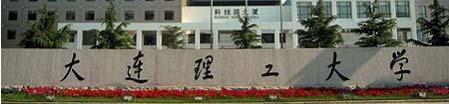
1 The 4th China-American Frontiers of Engineering Symposium Micro/nano and precision manufacturing technologies and applications Dazhi Wang School of Mechanical Engineering Dalian University of Technology Irvine, US Contact:
2 Outline Research background Research challenges Research progress Cross-scale manufacturing technology E-Jet micro/nano print-patterningpatterning Ultra precision grinding and chemical mechanical polishing technologies
3 Research background Made in China 2025 Premier Li Keqiang advanced the "Made in China 2025" concept in his Government Work Report. The major areas include: Biomedicine and high-performance medical apparatus Information technology Aerospace and aviation equipment Advanced rail equipment.. Manufacturing of high-performance parts and devices play an important role.


4 Research challenges of high-performance parts and devices The size has been decreased to micro- and nano-scale. The shape and structure become more complex and precise. The machining accuracy has been improved continuously. The material scope has been increased continuously. Microfluidic chips Flexible electronics Silicon wafer Grephene sensor It is difficult to satisfy the requirements of these parts and devices using conventional manufacturing technologies.
5 Research progress Cross-scale manufacturing technology E-Jet micro/nano print-patterning Ultra precision i grinding and chemical mechanical polishing technologies


 Key difficulties Controllable")
6 Cross-scale manufacturing technology Microfluidic chips have broad application prospects in rapid diagnosis of major diseases and personalized medicine. Micro-nano cross-scale structure and nano-structure are needed for special function such as filtering, block flowing. Microfluidic chips for diagnosis of myocardial infarction Genome mapping on nanofluidic chips (Nature Biotechnology, 2012) Key difficulties Controllable manufacturing of micro-nano cross-scale structure and special area nano-structure.


7 Cross-scale manufacturing technology A composited fabrication method based on plasma etching and nanoparticle assembly was proposed. Microchannel, nanochannel and modified biological sample were integrated fabricated. A high quality nanofluidic sensing of biotin was achieved, the concentration of 1 am can be detected. Fabrication of nanochannels and Ag microelectrodes Layout of the NPC-based nanofluidic biosensor Micro- and nanochannel and test result Biosensors and Bioelectronic, 2015


8 Cross-scale manufacturing technology An integration of hot embossing and inverse UV photolithography is developed to fabricate micro and nanochannels. A complete SU-8 nanofluidic chip was fabricated with a replication precision of 99.5%. Process flow of the 2D nano-mold fabrication SU-8 micro and nanochannels fabrication 130 nm wide, 150 nm high, 4 mm long 2D silicon nano-mold The thermally bonded nanochannels Lab on a chip, 2014


9 Cross-scale manufacturing technology A controllable fabrication of nanopores based on photopolymerization was proposed. Microfluidic idi chips with highh density nanopore array at specific area was realized. Glass micro-nanofluidic chips integrated with nano gel structure Photosensitive polymerization based on AC Impedance of Enrichment ratio of an inverted fluorescent microscope different nanopores fluorescence ions is 600 Applied Physics Letters, 2014
10 Cross-scale manufacturing technology Disease diagnosis microfluidic chips Cooperated with CapitalBio Corporation, detection of respiratory tract bacteria. Simultaneously detect 13 kinds of bacteria, detecting time reduced from 2 days to 3 hours, it is in clinical test now. 24-channel radial microchip Isothermal amplification & real-time fluorescent detector
11 E-Jet micro/nano print-patterning Multi-layer composite element commonly exists in MEMS devices, which are widely used in energy, information, medical treatment, etc. The performance of multi-layer composite MEMS devices was determined by their material composition and microstructure. Controllable fabrication of material and structural composited Key difficulties Controllable fabrication of material and structural composited fabrication.
12 E-Jet micro/nano print-patterning Print-patterning is an effective way to obtain the material and structural composited fabrication. Print-patterning is an additive manufacturing method and has the advantages of no mask, non-contact, no pressure and low cost. Flowing deformation Droplet flying Pattern Substrate Jetting Flying Deposition Solidification Print-patterning process Patterning MEMS devices


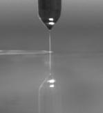
13 E-Jet micro/nano print-patterning Electrohydrodynamic effect was used to develop a new print-patterning tt i technology. Electrohydrodynamic jet (E-Jet) print- patterning makes use of electrical and mechanical forces to form a fine liquid jet and droplets. Needle Ink Substrate Jet Movement stage E-Jet print-patterning Phenomenon of electrohydrodynamic effect


14 E-Jet micro/nano print-patterning Advantages of E-Jet print-patterning High resolution Low requirement of needle and ink Strong controllability Suitable for different substrates Droplet diameter can be at nano-scale Droplet size is much smaller than needle Composite film deposition size: less than 1/100 Droplets are charged Non-contact patterning Mi / t t Micro/nano structure direct writing


")

15 E-Jet micro/nano print-patterning A layer-by-layer nano structure deposition method based on E- Jet was proposed. Material and structural composited fabrication with nano-scale layers were achieved. E-Jet deposition process 预测值实验值 Modeling of E-Jet deposition 孔隙隙率 ϕ Q P 1 α V f T L 1 ( H) f ( H) W 沉积高度 (10-3 m) Porosity prediction equation Deposition of catalyst layers with different porosity


16 E-Jet micro/nano print-patterning Template-assisted E-Jet deposition method combined with embossing sacrificial layer technology was developed. Complex microstructures with high side wall angle and high aspect ratio were achieved. Template-assisted assisted E-Jet Patterned PZT thick film deposition process Patterned graphene structures structures J. Eur. Ceram. Soc., 2012

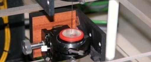
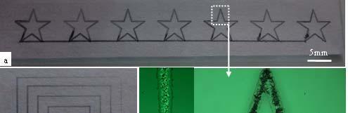
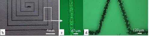
17 E-Jet micro/nano print-patterning A point focus electrode was used in E-Jet printing, which enabled the printing of structure in micro-scale resolution. 200μm E-Jet printing Point focusing electrode E-Jet print-patterning equipment E-Jet printed graphene structures E-Jet printed PZT structures Rev. Sci. Instrum., 2013, J. Eur. Ceram. Soc., 2015


 0.7 0.6 0.5 0.4 0.3 0.2 0.")

18 E-Jet micro/nano print-patterning Micro fuel cell: integrated MEA An integrated MEA was developed, the common delamination problem was solved, and the reliability of the device was improved. The catalyst layer with material and structure gradient variation was developed, the catalyst utilization was improved. arization / V IR corrected anode pola MEA1 MEA2 MEA Current density / A cm -2 Gas-liquid two-phase model Mass transferring process Modeling of cell performance Voltage (V) MEA-1 MEA-2 MEA Power density (mw cm -2 ) Integrated MEA after life test Structure of integrated MEA Current density (ma cm -2 ) Cell performance test J. Power Sources, 2013, Fuel cells, 2014


19 E-Jet micro/nano print-patterning High frequency ultrasonic transducer Annular array high frequency piezoelectric ultrasonic transducer was designed and developed, which achieved a working frequency of 70 MHz. Annular array high frequency ultrasonic transducers Measurement of high frequency ultrasonic transducers piezoelectric micro transformer Measurement of transformer Sens. Actuator A-Phys. 2014


20 Ultra precision grinding and chemical mechanical polishing technologies Ultra precision grinding and chemical mechanical polishing technologies are widely used for obtaining ultra flat and ultra smooth surface, such as blank wafer flattening, wafer back thinning. Blank wafer flattening Wafer back thinning Key difficulties large size, nano-scale flatness, sub-nm roughness, low residual stresses and damage-free.


21 Ultra precision grinding and chemical mechanical polishing technologies A new ultra precision and low damage grinding g technology with soft abrasive grinding wheel was developed. Ultra smooth and low damage ground surface wafer was produced. Grinding mechanism Developed SAGW of SAGW Damage depth 170nm Ra= 3.8nm The wafer ground with diamond grinding wheel Damage depth 10nm Ra= 0.7nm The wafer ground with SAGW


 Comparison of")
22 Ultra precision grinding and chemical mechanical polishing technologies A full-automatic grinder was developed for 300 mm wafer. A ultra precision wafer grinding-polishing machine was developed. The first automatic ultra precision grinding machine for 300 mm wafer grinding in China Principle and process of back thinning integrated grinding and polishing for wafer with outer rim Silicon wafer Sapphire wafer SiC window Optical window Ultra precision wafer grinding-polishing machine (2-spindle, 2-worktable ) Comparison of thinned wafer with and without outer rim Thinned wafer thickness<50μm,ra<5nm


23 Ultra precision grinding and chemical mechanical polishing technologies KDP is soft-brittle, temperature sensitive, dissolved in water, which is a difficult-to-machine materials. Abrasive-free polishing slurry with water molecular cluster was developed. Ultra smooth and damage-free surface was obtained using micro water-dissolution and mechanical action of polishing pad. Watercluster brocken pad Natural dissolution Water cluster KDP slurry Developed polishing slurry Water-dissolution polishing surface
24 Summary Micro-nano cross-scale manufacturing technologies were introduced, microfluidic chips for disease diagnosis and biosensing were produced. E-Jet micro/nano print-patterning technique and equipment were developed, which enables the material and structural composited manufacturing at micro/nano scale. Ultra precision grinding and chemical mechanical polishing technologies were introduced, d ultra smooth and low damage surface wafer was produced.


25 Acknowledgments Many thanks for the support from:


26 You are welcome to visit us at DLUT!
Integrated measuring system for MEMS
 Integrated measuring system for MEMS Thermal characterization of gas flows under slip-flow regime Alice Vittoriosi May 16, 2011 I NSTITUTE FOR M ICRO P ROCESS E NGINEERING - T HERMAL P ROCESS E NGINEERING
Lecture 18: Microfluidic MEMS, Applications
 MECH 466 Microelectromechanical Systems University of Victoria Dept. of Mechanical Engineering Lecture 18: Microfluidic MEMS, Applications 1 Overview Microfluidic Electrokinetic Flow Basic Microfluidic
Table of Content. Mechanical Removing Techniques. Ultrasonic Machining (USM) Sputtering and Focused Ion Beam Milling (FIB)
 Sputtering and Focused Ion Beam Milling (FIB)") Table of Content Mechanical Removing Techniques Ultrasonic Machining (USM) Sputtering and Focused Ion Beam Milling (FIB) Ultrasonic Machining In ultrasonic machining (USM), also called ultrasonic grinding,
Table of Content Mechanical Removing Techniques Ultrasonic Machining (USM) Sputtering and Focused Ion Beam Milling (FIB) Ultrasonic Machining In ultrasonic machining (USM), also called ultrasonic grinding,
Nanotechnology Fabrication Methods.
 Nanotechnology Fabrication Methods. 10 / 05 / 2016 1 Summary: 1.Introduction to Nanotechnology:...3 2.Nanotechnology Fabrication Methods:...5 2.1.Top-down Methods:...7 2.2.Bottom-up Methods:...16 3.Conclusions:...19
Institute for Electron Microscopy and Nanoanalysis Graz Centre for Electron Microscopy
 Institute for Electron Microscopy and Nanoanalysis Graz Centre for Electron Microscopy Micromechanics Ass.Prof. Priv.-Doz. DI Dr. Harald Plank a,b a Institute of Electron Microscopy and Nanoanalysis, Graz
ME381 Introduction to MEMS
 ME381 Introduction to MEMS Term Project Dynamic Wettability Switching by Surface Roughness Effect Bo He Hang Cheng Hongzhou Jiang December 6 th, 2002 1 TABLE OF CONTENTS Abstract........1 Introduction......1
Micro Chemical Vapor Deposition System: Design and Verification
 Micro Chemical Vapor Deposition System: Design and Verification Q. Zhou and L. Lin Berkeley Sensor and Actuator Center, Department of Mechanical Engineering, University of California, Berkeley 2009 IEEE
Supplementary information for
 Supplementary information for Transverse electric field dragging of DNA in a nanochannel Makusu Tsutsui, Yuhui He, Masayuki Furuhashi, Rahong Sakon, Masateru Taniguchi & Tomoji Kawai The Supplementary
Nano Materials and Devices
 Nano Materials and Devices Professor Michael Austin Platform Technologies Research Institute Nano Materials and Devices Program Aim: to develop an integrated capability in nanotechnology Design and modelling
There's Plenty of Room at the Bottom
 There's Plenty of Room at the Bottom 12/29/1959 Feynman asked why not put the entire Encyclopedia Britannica (24 volumes) on a pin head (requires atomic scale recording). He proposed to use electron microscope
Fabrication and Characterization of High Performance Micro Impedance Inclinometer
 Fabrication and Characterization of High Performance Micro Impedance Inclinometer Chia-Yen Lee Department of Vehicle Engineering National Pingtung University of Science and Technology, Pingtung, Taiwan
Nanofluidics and 2D Materials Based Nanosensors. Ivan Vlassiouk Oak Ridge National Laboratory, TN, USA
 Nanofluidics and 2D Materials Based Nanosensors Ivan Vlassiouk Oak Ridge National Laboratory, TN, USA Outline What are nanosensors and why do we need them? Learning from Nature is the key! Microfluidics
F R A U N H O F E R I N
 FRAUNHOFER Institute FoR Electronic NAno systems ENAS System Packaging 1 2 3 4 5 The actual developments of micro and nano technologies are fascinating. Undoubted they are playing a key role in today s
EE C245 ME C218 Introduction to MEMS Design Fall 2007
 EE C245 ME C218 Introduction to MEMS Design Fall 2007 Prof. Clark T.-C. Nguyen Dept. of Electrical Engineering & Computer Sciences University of California at Berkeley Berkeley, CA 94720 Lecture 12: Mechanics
Multilayer Wiring Technology with Grinding Planarization of Dielectric Layer and Via Posts
 Tani et al.: Multilayer Wiring Technology with Grinding Planarization (1/6) [Technical Paper] Multilayer Wiring Technology with Grinding Planarization of Dielectric Layer and Via Posts Motoaki Tani, Kanae
Supplementary Figure 1 shows overall fabrication process and detailed illustrations are given
 Supplementary Figure 1. Pressure sensor fabrication schematics. Supplementary Figure 1 shows overall fabrication process and detailed illustrations are given in Methods section. (a) Firstly, the sacrificial
ESS 5855 Surface Engineering for. MicroElectroMechanicalechanical Systems. Fall 2010
 ESS 5855 Surface Engineering for Microelectromechanical Systems Fall 2010 MicroElectroMechanicalechanical Systems Miniaturized systems with integrated electrical and mechanical components for actuation
Structuring and bonding of glass-wafers. Dr. Anke Sanz-Velasco
 Structuring and bonding of glass-wafers Dr. Anke Sanz-Velasco Outline IMT Why glass? Components for life science Good bond requirements and evaluation Wafer bonding 1. Fusion bonding 2. UV-adhesive bonding
Epitaxial piezoelectric heterostructures for ultrasound micro-transducers
 15 th Korea-U.S. Forum on Nanotechnology Epitaxial piezoelectric heterostructures for ultrasound micro-transducers Seung-Hyub Baek Center for Electronic Materials Korea Institute of Science and Technology
Research Article Apparatus Developments of Ultrasonic Vibration-Assisted Microabrasive Waterjet Polishing
 Materials Science and Engineering Volume 2018, Article ID 1742315, 9 pages https://doi.org/10.1155/2018/1742315 Research Article Apparatus Developments of Ultrasonic -Assisted Microabrasive Waterjet Polishing
Development and Characterization of High Frequency Bulk Mode Resonators
 Excerpt from the Proceedings of the COMSOL Conference 008 Hannover Development and Characterization of High Frequency Bulk Mode Resonators Hossein Pakdast 1*, Zachary James Davis 1 1 DTU Nanotech, Technical
EV Group. Engineered Substrates for future compound semiconductor devices
 EV Group Engineered Substrates for future compound semiconductor devices Engineered Substrates HB-LED: Engineered growth substrates GaN / GaP layer transfer Mobility enhancement solutions: III-Vs to silicon
Introduction to Micro/Nanofluidics. Date: 2015/03/13. Dr. Yi-Chung Tung. Outline
 Introduction to Micro/Nanofluidics Date: 2015/03/13 Dr. Yi-Chung Tung Outline Introduction to Microfluidics Basic Fluid Mechanics Concepts Equivalent Fluidic Circuit Model Conclusion What is Microfluidics
SINGLE-STEP ASSEMBLY OF COMPLEX 3-D MICROSTRUCTURES
 SINGLE-STEP ASSEMBLY OF COMPLEX 3-D MICROSTRUCTURES Elliot E. Hui, Roger T. Howe, and M. Steven Rodgers* Berkeley Sensor & Actuator Center, University of California, Berkeley, CA 94720-1774, USA *Intelligent
Regents of the University of California
 Deep Reactive-Ion Etching (DRIE) DRIE Issues: Etch Rate Variance The Bosch process: Inductively-coupled plasma Etch Rate: 1.5-4 μm/min Two main cycles in the etch: Etch cycle (5-15 s): SF 6 (SF x+ ) etches
OPTIMIZATION OF DIELECTRICS SURFACE PREPARATION FOR VACUUM COATING
 OPTIMIZATION OF DIELECTRICS SURFACE PREPARATION FOR VACUUM COATING Dr. Boris Statnikov Introduction Modern MICRO and NANO technologies in ultra- and high-frequency electronics are widely focused on application
Dynamic Strain of Ultrasonic Cu and Au Ball Bonding Measured In-Situ by Using Silicon Piezoresistive Sensor
 2017 IEEE 67th Electronic Components and Technology Conference Dynamic Strain of Ultrasonic Cu and Au Ball Bonding Measured In-Situ by Using Silicon Piezoresistive Sensor Keiichiro Iwanabe, Kenichi Nakadozono,
Nano-mechatronics. Presented by: György BudaváriSzabó (X0LY4M)
") Nano-mechatronics Presented by: György BudaváriSzabó (X0LY4M) Nano-mechatronics Nano-mechatronics is currently used in broader spectra, ranging from basic applications in robotics, actuators, sensors,
Nano-mechatronics Presented by: György BudaváriSzabó (X0LY4M) Nano-mechatronics Nano-mechatronics is currently used in broader spectra, ranging from basic applications in robotics, actuators, sensors,
Nanostructures Fabrication Methods
 Nanostructures Fabrication Methods bottom-up methods ( atom by atom ) In the bottom-up approach, atoms, molecules and even nanoparticles themselves can be used as the building blocks for the creation of
Nanostructured sensors. Raphaël Pugin Section Head Nanoscale Technology
 Nanostructured sensors Raphaël Pugin Section Head Nanoscale Technology Why nanostructures? Adhesion & wettability Optics Photovoltaics Sensors CSEM s DID Superhydrophobicity Anti-icing Dry-adhesion Friction
Piezoelectric Resonators ME 2082
 Piezoelectric Resonators ME 2082 Introduction K T : relative dielectric constant of the material ε o : relative permittivity of free space (8.854*10-12 F/m) h: distance between electrodes (m - material
ARC-ASSISTED CO-CONVERSION OF COAL-BASED CARBON AND ACETYLENE
 ARC-ASSISTED CO-CONVERSION OF COAL-BASED CARBON AND ACETYLENE Jieshan Qiu*, Yongfeng Li, Yunpeng Wang Carbon Research Laboratory, Center for Nano Materials and Science, School of Chemical Engineering,
Wafer bonding. Supplementary Figure 1. Conventional nanofluidic sealing process. (a) Selective sealing. (b) Wafer bonding. (c) Sacrificial etching.
 Selective sealing. (b) Wafer bonding. (c) Sacrificial etching.") (a) (b) (c) Selective sealing Wafer bonding Sacrificial etching Supplementary Figure 1. Conventional nanofluidic sealing process. (a) Selective sealing. (b) Wafer bonding. (c) Sacrificial etching. Supplementary
(a) (b) (c) Selective sealing Wafer bonding Sacrificial etching Supplementary Figure 1. Conventional nanofluidic sealing process. (a) Selective sealing. (b) Wafer bonding. (c) Sacrificial etching. Supplementary
NPTEL. Instability and Patterning of Thin Polymer Films - Video course. Chemical Engineering.
 NPTEL Syllabus Instability and Patterning of Thin Polymer Films - Video course COURSE OUTLINE T h i s course will expose students to the science of sub-micron, meso and nanoscale patterning of surfaces
LAYER BY LAYER (LbL) SELF-ASSEMBLY STRATEGY AND ITS APPLICATIONS
 SELF-ASSEMBLY STRATEGY AND ITS APPLICATIONS") LAYER BY LAYER (LbL) SELF-ASSEMBLY STRATEGY AND ITS APPLICATIONS A. Z. Cheng 1, R. Swaminathan 2 1 Nanotechnology Engineering, University of Waterloo, azcheng@uwaterloo.ca; 2 Nanotechnology Engineering,
LAYER BY LAYER (LbL) SELF-ASSEMBLY STRATEGY AND ITS APPLICATIONS A. Z. Cheng 1, R. Swaminathan 2 1 Nanotechnology Engineering, University of Waterloo, azcheng@uwaterloo.ca; 2 Nanotechnology Engineering,
Fabrication and performance of d 33 -mode lead-zirconate-titanate (PZT) MEMS accelerometers
 MEMS accelerometers") Fabrication and performance of d 33 -mode lead-zirconate-titanate (PZT) MEMS accelerometers H. G. Yu, R. Wolf*,K. Deng +,L.Zou +, S. Tadigadapa and S. Trolier-McKinstry* Department of Electrical Engineering,
Fabrication and performance of d 33 -mode lead-zirconate-titanate (PZT) MEMS accelerometers H. G. Yu, R. Wolf*,K. Deng +,L.Zou +, S. Tadigadapa and S. Trolier-McKinstry* Department of Electrical Engineering,
GHZ ELECTRICAL PROPERTIES OF CARBON NANOTUBES ON SILICON DIOXIDE MICRO BRIDGES
 GHZ ELECTRICAL PROPERTIES OF CARBON NANOTUBES ON SILICON DIOXIDE MICRO BRIDGES SHENG F. YEN 1, HAROON LAIS 1, ZHEN YU 1, SHENGDONG LI 1, WILLIAM C. TANG 1,2, AND PETER J. BURKE 1,2 1 Electrical Engineering
LMM-H04 Mass Air Flow Sensor
 Hot Film Anemometer Component Highly reliable and long term stable Uni-directional airflow measurement Fast reaction time Manufactured according ISO TS16949 Can be adapted to various flow channel geometries
Nanostrukturphysik (Nanostructure Physics)
") Nanostrukturphysik (Nanostructure Physics) Prof. Yong Lei & Dr. Yang Xu Fachgebiet 3D-Nanostrukturierung, Institut für Physik Contact: yong.lei@tu-ilmenau.de; yang.xu@tu-ilmenau.de Office: Unterpoerlitzer
Nanostrukturphysik (Nanostructure Physics) Prof. Yong Lei & Dr. Yang Xu Fachgebiet 3D-Nanostrukturierung, Institut für Physik Contact: yong.lei@tu-ilmenau.de; yang.xu@tu-ilmenau.de Office: Unterpoerlitzer
Stretchable Graphene Transistors with Printed Dielectrics and Gate Electrodes
 Stretchable Graphene Transistors with Printed Dielectrics and Gate Electrodes Seoung-Ki Lee, Beom Joon Kim, Houk Jang, Sung Cheol Yoon, Changjin Lee, Byung Hee Hong, John A. Rogers, Jeong Ho Cho, Jong-Hyun
Especial Bump Bonding Technique for Silicon Pixel Detectors
 Especial Bump Bonding Technique for Silicon Pixel Detectors E. Cabruja, M. Bigas, M. Ullán, G. Pellegrini, M. Lozano Centre Nacional de Microelectrònica Spain Outline Motivation Summary of bump bonding
MSN551 LITHOGRAPHY II
 MSN551 Introduction to Micro and Nano Fabrication LITHOGRAPHY II E-Beam, Focused Ion Beam and Soft Lithography Why need electron beam lithography? Smaller features are required By electronics industry:
Gold Nanoparticles Floating Gate MISFET for Non-Volatile Memory Applications
 Gold Nanoparticles Floating Gate MISFET for Non-Volatile Memory Applications D. Tsoukalas, S. Kolliopoulou, P. Dimitrakis, P. Normand Institute of Microelectronics, NCSR Demokritos, Athens, Greece S. Paul,
Fast Biofluid Transport of High Conductive Liquids Using AC Electrothermal Phenomenon, A Study on Substrate Characteristics
 Fast Biofluid Transport of High Conductive Liquids Using AC Electrothermal Phenomenon, A Study on Substrate Characteristics A. Salari, C. Dalton Department of Electrical & Computer Engineering, University
J. G. Eden. University of Illinois. University of Illinois. Laboratory for Optical Physics and Engineering
 NEW OPPORTUNITIES IN PHOTONICS APPLICATIONS : MICROPLASMA DEVICES AND ARRAYS FABRICATED IN SEMICONDUCTORS, CERAMIC AND POLYMER/METAL MULTILAYER STRUCTURES J. G. Eden MICROPLASMAS: AT THE INTERSECTION OF
Nanoscale Issues in Materials & Manufacturing
 Nanoscale Issues in Materials & Manufacturing ENGR 213 Principles of Materials Engineering Module 2: Introduction to Nanoscale Issues Top-down and Bottom-up Approaches for Fabrication Winfried Teizer,
Foundations of MEMS. Chang Liu. McCormick School of Engineering and Applied Science Northwestern University. International Edition Contributions by
 Foundations of MEMS Second Edition Chang Liu McCormick School of Engineering and Applied Science Northwestern University International Edition Contributions by Vaishali B. Mungurwadi B. V. Bhoomaraddi
Wafer-scale fabrication of graphene
 Wafer-scale fabrication of graphene Sten Vollebregt, MSc Delft University of Technology, Delft Institute of Mircosystems and Nanotechnology Delft University of Technology Challenge the future Delft University
Report on Visit to Ruhr University Bochum by International Training Program From October 1st to November 29th 2010
 Report on Visit to Ruhr University Bochum by International Training Program From October 1st to November 29th 2010 Graduate school of Engineering, Hori-Sekine Lab. Doctor course student Yusuke Abe Ruhr
Ultrasonic particle and cell separation and size sorting
 SMR.1670-25 INTRODUCTION TO MICROFLUIDICS 8-26 August 2005 Ultrasonic Particle and Cell Separation and Size Sorting in Micro-channels V. Steinberg Weizmann Institute of Science, Israel Ultrasonic particle
Comparative Assessment of the Transient Temperature Response during Single-discharge Machining by Micro-EDM and LIP-MM Processes
 Comparative Assessment of the Transient Temperature Response during Single-discharge Machining by Micro-EDM and LIP-MM Processes ICOMM 2014 No. 37 Ishan Saxena #1, Xiaochun Li 2, K. F. Ehmann 1 1 Department
NSC E
 NSC 892218E006071 1 Preparation of NSC Project Reports microfluidic channels are fabricated on quartz substrates and then used to imprint microstructures into Polymethylmethacrylate (PMMA) substrates using
Temporary Wafer Bonding - Key Technology for 3D-MEMS Integration
 Temporary Wafer Bonding - Key Technology for 3D-MEMS Integration 2016-06-15, Chemnitz Chemnitz University of Technology Basic Research Fraunhofer ENAS System-Packaging (SP) Back-End of Line (BEOL) Applied
MICRO AND NANOPROCESSING TECHNOLOGIES
 LECTURE 5 MICRO AND NANOPROCESSING TECHNOLOGIES Introduction Ion lithography X-ray lithography Soft lithography E-beam lithography Concepts and processes Lithography systems Masks and resists Chapt.9.
20 MHz Free-Free Beam Microelectromechanical Filter with High Quality Factor
 20 MHz Free-Free Beam Microelectromechanical Filter with High Quality Factor Group 4 Yang Lu 1, Tianfeng Lu 1, Han Wang 2, Zichen Tang 2 1 Department of Material Science and Engineering 2 Department of
Thin Wafer Handling Debonding Mechanisms
 Thin Wafer Handling Debonding Mechanisms Jonathan Jeauneau, Applications Manager Alvin Lee, Technology Strategist Dongshun Bai, Scientist, 3-D IC R&D Materials Outline Requirements of Thin Wafer Handling
2.76/2.760 Multiscale Systems Design & Manufacturing
 2.76/2.760 Multiscale Systems Design & Manufacturing Fall 2004 MOEMS Devices for Optical communications system Switches and micromirror for Add/drops Diagrams removed for copyright reasons. MOEMS MEMS
Surface Acoustic Wave Atomizer with Pumping Effect
 Surface Acoustic Wave Atomizer with Pumping Effect Minoru KUROSAWA, Takayuki WATANABE and Toshiro HIGUCHI Dept. of Precision Machinery Engineering, Faculty of Engineering, University of Tokyo 7-3-1 Hongo,
process dependencies in nanoimprint
 Modeling and mitigating pattern and process dependencies in nanoimprint lithography 23 June 2011 Hayden Taylor Singapore-MIT Alliance for Research and Technology formerly based at: Microsystems Technology
Porous silicon as base material of MEMS-compatible fuel cell components
 Porous silicon as base material of MEMS-compatible fuel cell components José Geraldo Alves Brito Neto Tokyo University of Science - Faculty of Science and Technology Department of Mechanical Engineering
Chapter 3 Engineering Science for Microsystems Design and Fabrication
 Lectures on MEMS and MICROSYSTEMS DESIGN and MANUFACTURE Chapter 3 Engineering Science for Microsystems Design and Fabrication In this Chapter, we will present overviews of the principles of physical and
DQN Positive Photoresist
 UNIVESITY OF CALIFONIA, BEKELEY BEKELEY DAVIS IVINE LOS ANGELES IVESIDE SAN DIEGO SAN FANCISCO SANTA BABAA SANTA CUZ DEPATMENT OF BIOENGINEEING 94720-1762 BioE 121 Midterm #1 Solutions BEKELEY, CALIFONIA
FRAUNHOFER INSTITUTE FOR SURFACE ENGINEERING AND THIN FILMS IST ATMOSPHERIC PRESSURE PLASMA PROCESSES
 FRAUNHOFER INSTITUTE FOR SURFACE ENGINEERING AND THIN FILMS IST ATMOSPHERIC PRESSURE PLASMA PROCESSES 1 2 ATMOSPHERIC PRESSURE PLASMA PROCESSES AT THE FRAUNHOFER IST Today, atmospheric pressure plasma
DESIGN AND FABRICATION OF THE MICRO- ACCELEROMETER USING PIEZOELECTRIC THIN FILMS
 DESIGN AND FABRICATION OF THE MICRO- ACCELEROMETER USING PIEZOELECTRIC THIN FILMS JYH-CHENG YU and FU-HSIN LAI Department of Mechanical Engineering National Taiwan University of Science and Technology
Enhanced performance of microbolometer. using coupled feed horn antenna
 Enhanced performance of microbolometer using coupled feed horn antenna Kuntae Kim*,a, Jong-Yeon Park*, Ho-Kwan Kang*, Jong-oh Park*, Sung Moon*, Jung-ho Park a * Korea Institute of Science and Technology,
The Characterization of Nanoparticle Element Oxide Slurries Used in Chemical-Mechanical Planarization by Single Particle ICP-MS
 A P P L I C AT I O N N O T E ICP - Mass Spectrometry Authors: Lee Davidowski Chady Stephan PerkinElmer, Inc. Shelton, CT The Characterization of Nanoparticle Element Oxide Slurries Used in Chemical-Mechanical
A vibrating micro-cmm probe for micropart metrology
 Microparts meeting - NPL 28 th October 2009 A vibrating micro-cmm probe for micropart metrology Richard Leach A vibrating micro-cmm probe for micro-part metrology Introduction Measuring co-ordinate geometry
Hybrid Wafer Level Bonding for 3D IC
 Hybrid Wafer Level Bonding for 3D IC An Equipment Perspective Markus Wimplinger, Corporate Technology Development & IP Director History & Roadmap - BSI CIS Devices???? 2013 2 nd Generation 3D BSI CIS with
Revealing High Fidelity of Nanomolding Process by Extracting the Information from AFM Image with Systematic Artifacts
 Revealing High Fidelity of Nanomolding Process by Extracting the Information from AFM Image with Systematic Artifacts Sajal Biring* Department of Electronics Engineering and Organic Electronics Research
MICRO-SCALE SHEET RESISTANCE MEASUREMENTS ON ULTRA SHALLOW JUNCTIONS
 MICRO-SCALE SHEET RESISTANCE MEASUREMENTS ON ULTRA SHALLOW JUNCTIONS Christian L. Petersen, Rong Lin, Dirch H. Petersen, Peter F. Nielsen CAPRES A/S, Burnaby, BC, Canada CAPRES A/S, Lyngby, Denmark We
Supplementary Figure 1 Detailed illustration on the fabrication process of templatestripped
 Supplementary Figure 1 Detailed illustration on the fabrication process of templatestripped gold substrate. (a) Spin coating of hydrogen silsesquioxane (HSQ) resist onto the silicon substrate with a thickness
Anti-icing surfaces based on enhanced self-propelled jumping of condensed water microdroplets
 Anti-icing surfaces based on enhanced self-propelled jumping of condensed water microdroplets Qiaolan Zhang, a,b Min He, a Jing Chen, a,b Jianjun Wang,* a Yanlin Song* a and Lei Jiang a a Beijing National
The Effects of Operating Parameters on Micro-Droplet Formation in a Piezoelectric Inkjet Printhead Using a Double Pulse Voltage Pattern
 Materials Transactions, Vol. 47, No. 2 (2006) pp. 375 to 382 #2006 The Japan Institute of Metals The Effects of Operating Parameters on Micro-Droplet Formation in a Piezoelectric Inkjet Printhead Using
Figure 1: Graphene release, transfer and stacking processes. The graphene stacking began with CVD
 Supplementary figure 1 Graphene Growth and Transfer Graphene PMMA FeCl 3 DI water Copper foil CVD growth Back side etch PMMA coating Copper etch in 0.25M FeCl 3 DI water rinse 1 st transfer DI water 1:10
Outline. Chemical Microsystems Applications. Microfluidic Component Examples Chemical Microsystems for Analysis Chemical Microsystems for Synthesis
 Outline Chemical Microsystems Applications Microfluidic Component Examples Chemical Microsystems for Analysis Chemical Microsystems for Synthesis Fundamentals of Micromachining Dr. Bruce Gale With Special
Modeling of an Acoustic Microfluidic Trap
 Washington University in St. Louis Washington University Open Scholarship Mechanical Engineering and Materials Science Independent Study Mechanical Engineering & Materials Science 5-11-2017 Modeling of
The goal of this project is to enhance the power density and lowtemperature efficiency of solid oxide fuel cells (SOFC) manufactured by atomic layer
 manufactured by atomic layer") Stanford University Michael Shandalov1, Shriram Ramanathan2, Changhyun Ko2 and Paul McIntyre1 1Department of Materials Science and Engineering, Stanford University 2Division of Engineering and Applied
Stanford University Michael Shandalov1, Shriram Ramanathan2, Changhyun Ko2 and Paul McIntyre1 1Department of Materials Science and Engineering, Stanford University 2Division of Engineering and Applied
Microfluidic biosensor for single cell high speed flow impedance spectroscopy
 Microfluidic biosensor for single cell high speed flow impedance spectroscopy J. Claudel, M. Nadi, O. Elmazria, D. Kourtiche Institut Jean Lamour (UMR 7198), CNRS (UMR7189) Université de Lorraine Vandoeuvre
Large Scale Direct Synthesis of Graphene on Sapphire and Transfer-free Device Fabrication
 Supplementary Information Large Scale Direct Synthesis of Graphene on Sapphire and Transfer-free Device Fabrication Hyun Jae Song a, Minhyeok Son a, Chibeom Park a, Hyunseob Lim a, Mark P. Levendorf b,
Sensor Measurements For Diagnostic Equipment
 Sensor Measurements For Diagnostic Equipment Mossi, K. Virginia Commonwealth University 601 West Main Street, Room 318 Richmond, VA 23284 kmmossi@vcu.edu (804) 827-5275 Scott, L.A. Dominion Energy, Inc.
Simulation Analysis of Microchannel Deformation during LTCC Warm Water Isostatic Pressing Process Lang Ping, Zhaohua Wu*
 International Conference on Information Sciences, Machinery, Materials and Energy (ICISMME 2015) Simulation Analysis of Microchannel Deformation during LTCC Warm Water Isostatic Pressing Process Lang Ping,
ESH Benign Processes for he Integration of Quantum Dots (QDs)
") ESH Benign Processes for he Integration of Quantum Dots (QDs) PIs: Karen K. Gleason, Department of Chemical Engineering, MIT Graduate Students: Chia-Hua Lee: PhD Candidate, Department of Material Science
ESH Benign Processes for he Integration of Quantum Dots (QDs) PIs: Karen K. Gleason, Department of Chemical Engineering, MIT Graduate Students: Chia-Hua Lee: PhD Candidate, Department of Material Science
Time-of-Flight Flow Microsensor using Free-Standing Microfilaments
 07-Rodrigues-V4 N2-AF 19.08.09 19:41 Page 84 Time-of-Flight Flow Microsensor using Free-Standing Microfilaments Roberto Jacobe Rodrigues 1,2, and Rogério Furlan 3 1 Center of Engineering and Social Sciences,
Chip-Scale Mass Spectrometers for Portable Gas Analyzers Luis Fernando Velásquez-García. A. I. Akinwande, K. Cheung, and L.-Y Chen.
 Chip-Scale Mass Spectrometers for Portable Gas Analyzers Luis Fernando Velásquez-García. A. I. Akinwande, K. Cheung, and L.-Y Chen. Microsystems Technology Laboratories (MTL) lfvelasq@mit.edu November
EE C245 ME C218 Introduction to MEMS Design Fall 2007
 EE C245 ME C218 Introduction to MEMS Design Fall 2007 Prof. Clark T.-C. Nguyen Dept. of Electrical Engineering & Computer Sciences University of California at Berkeley Berkeley, CA 94720 Lecture 11: Bulk
Quantum Dots for Advanced Research and Devices
 Quantum Dots for Advanced Research and Devices spectral region from 450 to 630 nm Zero-D Perovskite Emit light at 520 nm ABOUT QUANTUM SOLUTIONS QUANTUM SOLUTIONS company is an expert in the synthesis
Mechanical characterization of single crystal BaTiO 3 film and insitu. XRD observation of microstructure change due to
 76 Chapter 4 Mechanical characterization of single crystal BaTiO 3 film and insitu XRD observation of microstructure change due to mechanical loading 4.1 Introduction Ferroelectric materials have many
Kavli Workshop for Journalists. June 13th, CNF Cleanroom Activities
 Kavli Workshop for Journalists June 13th, 2007 CNF Cleanroom Activities Seeing nm-sized Objects with an SEM Lab experience: Scanning Electron Microscopy Equipment: Zeiss Supra 55VP Scanning electron microscopes
Hydrodynamics of Diamond-Shaped Gradient Nanopillar Arrays for Effective. DNA Translocation into Nanochannels. (Supplementary information)
") Hydrodynamics of Diamond-Shaped Gradient Nanopillar Arrays for Effective DNA Translocation into Nanochannels (Supplementary information) Chao Wang 1, Robert L. Bruce, Elizabeth A. Duch, Jyotica V. Patel,
Hydrodynamics of Diamond-Shaped Gradient Nanopillar Arrays for Effective DNA Translocation into Nanochannels (Supplementary information) Chao Wang 1, Robert L. Bruce, Elizabeth A. Duch, Jyotica V. Patel,
Deposition of Multilayer Fibers and Beads by Near-Field Electrospinning for Texturing and 3D Printing Applications
 Deposition of Multilayer Fibers and Beads by Near-Field Electrospinning for Texturing and 3D Printing Applications Nicolas Martinez-Prieto, Jian Cao, and Kornel Ehmann Northwestern University SmartManufacturingSeries.com
Lecture 0: Introduction
 Lecture 0: Introduction Introduction q Integrated circuits: many transistors on one chip q Very Large Scale Integration (VLSI): bucketloads! q Complementary Metal Oxide Semiconductor Fast, cheap, low power
Title Single Row Nano-Tribological Printing: A novel additive manufacturing method for nanostructures
 Nano-Tribological Printing: A novel additive manufacturing method for nanostructures H.S. Khare, N.N. Gosvami, I. Lahouij, R.W. Carpick hkhare@seas.upenn.edu carpick@seas.upenn.edu carpick.seas.upenn.edu
The solution for all of your
 The solution for all of your nanoparticle sizing and zeta potential needs. DelsaNano Series Blood Banking Capillary Electrophoresis Cell Analysis Centrifugation Genomics Lab Automation Lab Tools Particle
Control of Manufacturing Process
 Control of Manufacturing Process Subject 2.830 Spring 2004 Lecture #2 Process Modeling for Control February 5, 2004 Key Topics Process Taxonomy for Control Classifying the Universe of Processes Control
Solid State Physics (condensed matter): FERROELECTRICS
: FERROELECTRICS") Solid State Physics (condensed matter): FERROELECTRICS Prof. Igor Ostrovskii The University of Mississippi Department of Physics and Astronomy Oxford, UM: May, 2012 1 People: Solid State Physics Condensed
Solid State Physics (condensed matter): FERROELECTRICS Prof. Igor Ostrovskii The University of Mississippi Department of Physics and Astronomy Oxford, UM: May, 2012 1 People: Solid State Physics Condensed
Woo Jin Hyun, Ethan B. Secor, Mark C. Hersam, C. Daniel Frisbie,* and Lorraine F. Francis*
 Woo Jin Hyun, Ethan B. Secor, Mark C. Hersam, C. Daniel Frisbie,* and Lorraine F. Francis* Dr. W. J. Hyun, Prof. C. D. Frisbie, Prof. L. F. Francis Department of Chemical Engineering and Materials Science
Fabrication of micro-optical components in polymer using proton beam micro-machining and modification
 Nuclear Instruments and Methods in Physics Research B 210 (2003) 250 255 www.elsevier.com/locate/nimb Fabrication of micro-optical components in polymer using proton beam micro-machining and modification
Modeling of MEMS Fabrication Processes
 Modeling of MEMS Fabrication Processes Prof. Duane Boning Microsystems Technology Laboratories Electrical Engineering and Computer Science Massachusetts Institute of Technology September 28, 2007 Spatial
Active Plasmonic Nanostructures in Biosensing and Imaging. Bjoern M. Reinhard Department of Chemistry
 Active Plasmonic Nanostructures in Biosensing and Imaging Bjoern M. Reinhard Department of Chemistry Noble Metal Nanoparticles Light The alternating surface charges effectively form an oscillating dipole,
CURRENT STATUS OF NANOIMPRINT LITHOGRAPHY DEVELOPMENT IN CNMM
 U.S. -KOREA Forums on Nanotechnology 1 CURRENT STATUS OF NANOIMPRINT LITHOGRAPHY DEVELOPMENT IN CNMM February 17 th 2005 Eung-Sug Lee,Jun-Ho Jeong Korea Institute of Machinery & Materials U.S. -KOREA Forums