Nano fabrication and optical characterization of nanostructures
|
|
|
- Suzan Taylor
- 5 years ago
- Views:
Transcription
1 Introduction to nanooptics, Summer Term 2012, Abbe School of Photonics, FSU Jena, Prof. Thomas Pertsch Nano fabrication and optical characterization of nanostructures Lecture 12 1
2 Optical characterization methods VIS/NIR spectrophotometry (175 nm nm, 1x1mm, angle resolved) FTIR spectroscopy (200nm nm, 1x1mm, angle resolved) spatially resolved spectroscopy with microscope spectrometers (320 nm nm, 10x10µm or VIS 1x1µm) single particle/metaatom spectroscopy (VIS) white light interferometry for measurement of complex parameters ( nm, 2x2mm) SNOM - nearfield scanning microscopy (aperture / scattering / two-tip in VIS/NIR) single photon time correlated microscopy (VIS/NIR, 10 ps resolution) PEEM - photoemission electron microscopy: imaging & spectroscopy (resolution: spatial 20nm, energy 100meV, temporal <15fs)

3 3 Motivation Retrieval of effective parameters R Re Circular dichroism Circular birefringence Refractive index & impedance or Permittivity & Permeability
4 4 White light interferometry
5 5 Experimental method White light Fourier-transform spectroscopy in frequency space Fouriertransformation
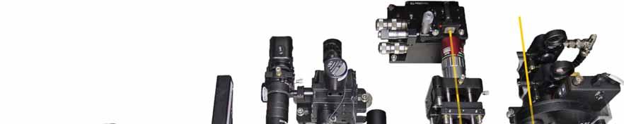
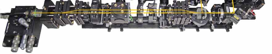
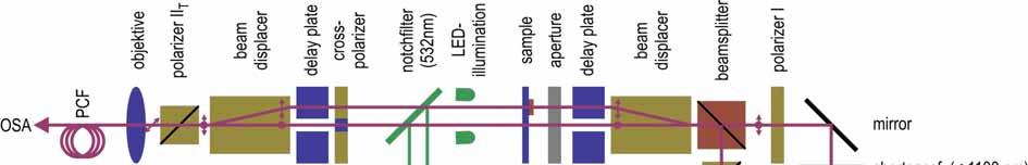
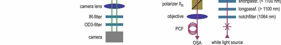
6 6 Characterization instrument OSA: Yokogawa AQ6370B WLS: NKT SuperK EXW-6 bandwidth: nm
7 7 Exemplary results


8 8 Exemplary results Fishnet


![[nm] [nm]](/docs-images/84/89180069/images/9-3.jpg)
9 9 Exemplary results Fishnet - measurements wavelength [nm] wavelength [nm] wavelength [nm] wavelength [nm]


![wavelength [nm]](/docs-images/84/89180069/images/10-3.jpg)
10 10 Exemplary results Fishnet effective parameter retrieval 0,2 wavelength [nm] wavelength [nm] wavelength [nm] wavelength [nm]
11 11 Spatially resolved spectroscopy


12 Annealed silver Negative index metamaterial

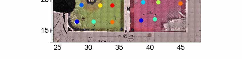
13 Space-resolved R and T measurements Bruker Vertex 80v (spectrometer) Hyperion 2000 (microscope) Wavelength range: 300 nm 16 µm Resolution: 0,07 cm -1 0,7 pm - 1,8 nm Mag.: 15x NA: 0.4 (~23,6 ) Spot: ~(250 µm)²

14 T/R/A-Measurements at different positions Absorption Reflectance Transmitance
15 15 Characterization of single metaatoms
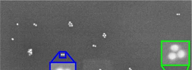
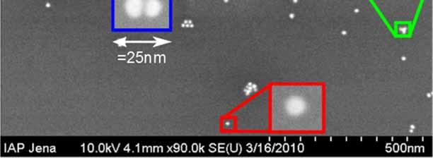
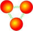
16 16 Self-assembled nanoparticles SEM measurements 11nm Au spheres dimer trimer quadromer
17 Nanoparticles detection methods Min. size of nanoparticle 40 nm 10 nm 5 nm 2.5 nm Dark field microscopy Attenuated total reflectance microscopy Nonlinear signal detection: THG Interferometric optical detection Modulating the sample positions Photothermal imaging (interference contrast and heterodyne detection) 1 7
 y 2 ext 2 I 2 sin 2 y 2 (2 ft) DC Component at fundamental Frequency (T1) Component at second Harmonic (T2) Phys. Rev. Lett.")
18 Nanoparticle optical detection by lateral modulation of sample position P exti( x, y0 sin 2 ft) particle oscillates in the focus P ext I( x, y) ext I sin(2 ft) y 2 ext 2 I 2 sin 2 y 2 (2 ft) DC Component at fundamental Frequency (T1) Component at second Harmonic (T2) Phys. Rev. Lett. 93, 2, 2004


19 Experimental setup x z y Illumination: solid state lasers, and white light source Modulation frequency f=860hz Detection: PMT and Lock-in amplifier in phase with modulation of sample.


20 Test measurements Gold colloids with diameters of 20, 40, and 80 nm from British Biocell was mixed in ethanol in ratio of 1:1:1:200 Particles deposited on 160µm cover slip ethanol 20nm 40nm 80nm 200 : 1 : 1 : 1 Image of sample in dark-field microscope 2 0

21 Test measurements Image of the X component Optical mapping of the transmission at λ = 561 nm recorded at fundamental frequency f=860hz.
22 Nano technology: challenges Properties strong interaction of light need strong polarizability high density of free electrons noble metals (Au, Ag) + Al mesoscopic dimensions of structures (~ 100 nm) hierarchical strongly broken symmetries on multiple length scales Challenges needed complex nano-scaled order principles are not compatible with the isotropic, short ranging character of bonding forces in strongly polarizable media (metal bonds) often thermodynamic metastable states (shallow local energetic minimum) or even unstable states (no energetic minimum) practical stabilization of matter by kinetic slow down of conversion towards stable thermodynamic phase (practically long time scales)

 Substrate BOTTOM UP")


23 Nano-Optics technological approaches TOP DOWN EBL Exposure Resist Funct. Layer(s) Substrate BOTTOM UP diblock copolymer unloaded micelle Development loaded micelle Resist Pattern pulling from solution Dry Etching monolayer Removal of Resist oxygen plasma Final Element gold nanostructure
24 Nano-Optics typical top down technologies lithographic techniques Electron Beam Lithography (EBL) Focused Ion Beam milling (FIB) holographic 3D lithography / multi-photon laser polymerization nano-tip-lithography etching techniques deposition techniques sputtering, evaporation Chemical Vapor Deposition (CVD) Molecular Beam Epitaxy (MBE) atomic layer deposition (ALD) replication technologies Nano Imprint Lithographie (NIL) (XUV lithography, roll-to-roll replication) chemical inversion processes for 3D replication in different classes of materials fiber drawing techniques (low productivity reflects the state of these activities - fundamental research)
Nano fabrication by e-beam lithographie
 Introduction to nanooptics, Summer Term 2012, Abbe School of Photonics, FSU Jena, Prof. Thomas Pertsch Nano fabrication by e-beam lithographie Lecture 14 1 Electron Beam Lithography - EBL Introduction
Fundamentals of nanoscience
 Fundamentals of nanoscience Spectroscopy of nano-objects Mika Pettersson 1. Non-spatially resolved spectroscopy Traditionally, in spectroscopy, one is interested in obtaining information on the energy
Supporting Information
 Copyright WILEY VCH Verlag GmbH & Co. KGaA,69469 Weinheim,Germany,2011 Supporting Information for Small,DOI: 10.1002/ smll.201100371 Lithographically Fabricated Optical Antennas with Gaps Well Below 10
Supplementary Figure 1 Detailed illustration on the fabrication process of templatestripped
 Supplementary Figure 1 Detailed illustration on the fabrication process of templatestripped gold substrate. (a) Spin coating of hydrogen silsesquioxane (HSQ) resist onto the silicon substrate with a thickness
Laboratory lecture in Introduction to Nanooptics (2012 SS)
") INO12_lab_lecture_2012-07-13.docx 1 Laboratory lecture in Introduction to Nanooptics (2012 SS) by Prof. Thomas PERTSCH at Friedrich-Schiller-Universität Jena in summer term 2012 13 July, 2012, 12:45 15:15
INO12_lab_lecture_2012-07-13.docx 1 Laboratory lecture in Introduction to Nanooptics (2012 SS) by Prof. Thomas PERTSCH at Friedrich-Schiller-Universität Jena in summer term 2012 13 July, 2012, 12:45 15:15
Demonstration of Near-Infrared Negative-Index Materials
 Demonstration of Near-Infrared Negative-Index Materials Shuang Zhang 1, Wenjun Fan 1, N. C. Panoiu 2, K. J. Malloy 1, R. M. Osgood 2 and S. R. J. Brueck 2 1. Center for High Technology Materials and Department
Nanostructures Fabrication Methods
 Nanostructures Fabrication Methods bottom-up methods ( atom by atom ) In the bottom-up approach, atoms, molecules and even nanoparticles themselves can be used as the building blocks for the creation of
Two-Photon Fabrication of Three-Dimensional Metallic Nanostructures for Plasmonic Metamaterials
 Two-Photon Fabrication of Three-Dimensional Metallic Nanostructures for Plasmonic Metamaterials Atsushi ISHIKAWA 1 and Takuo TANAKA 1,2 1- Metamaterials Laboratory, RIKEN, 2-1 Hirosawa, Wako, Saitama 351-0198,
Università degli Studi di Bari "Aldo Moro"
 Università degli Studi di Bari "Aldo Moro" Table of contents 1. Introduction to Atomic Force Microscopy; 2. Introduction to Raman Spectroscopy; 3. The need for a hybrid technique Raman AFM microscopy;
Supporting information:
 Supporting information: Wavevector-Selective Nonlinear Plasmonic Metasurfaces Kuang-Yu Yang, 1,# Ruggero Verre, 2, # Jérémy Butet, 1,#, * Chen Yan, 1 Tomasz J. Antosiewicz, 2,3 Mikael Käll, 2 and Olivier
Nanosphere Lithography
 Nanosphere Lithography Derec Ciafre 1, Lingyun Miao 2, and Keita Oka 1 1 Institute of Optics / 2 ECE Dept. University of Rochester Abstract Nanosphere Lithography is quickly emerging as an efficient, low
Supplementary Figure 1 SEM images and corresponding Fourier Transformation of nanoparticle arrays before pattern transfer (left), after pattern
, after pattern") Supplementary Figure 1 SEM images and corresponding Fourier Transformation of nanoparticle arrays before pattern transfer (left), after pattern transfer but before pattern shrinkage (middle), and after
Supplementary Figure 1 SEM images and corresponding Fourier Transformation of nanoparticle arrays before pattern transfer (left), after pattern transfer but before pattern shrinkage (middle), and after
Aluminum for nonlinear plasmonics: Methods Section
 Aluminum for nonlinear plasmonics: Methods Section Marta Castro-Lopez, Daan Brinks, Riccardo Sapienza, and Niek F. van Hulst, ICFO - Institut de Ciencies Fotoniques, and ICREA - Institució Catalana de
High-density data storage: principle
 High-density data storage: principle Current approach High density 1 bit = many domains Information storage driven by domain wall shifts 1 bit = 1 magnetic nanoobject Single-domain needed Single easy axis
Advanced Vitreous State The Physical Properties of Glass
 Advanced Vitreous State The Physical Properties of Glass Active Optical Properties of Glass Lecture 21: Nonlinear Optics in Glass-Applications Denise Krol Department of Applied Science University of California,
Development Of Spatial Modulation Spectroscopy Of Single Nano-Objects In Liquid Environments For Biosensing Applications
 title Development Of Spatial Modulation Spectroscopy Of ngle Nano-Objects In Liquid Environments For Biosensing Applications J-M. Rye 1,2, C. Bonnet 1, F. Lerouge 2, J. Lermé 1, A. Mosset 1, M. Broyer
Third-harmonic generation
 2 Third-harmonic generation 2.1 Introduction Optical signals from single nano-objects open new windows for studies at nanometer scales in fields as diverse as material science and cell biology. Cleared
Advanced techniques Local probes, SNOM
 Advanced techniques Local probes, SNOM Principle Probe the near field electromagnetic field with a local probe near field probe propagating field evanescent Advanced techniques Local probes, SNOM Principle
Optical Spectroscopy of Advanced Materials
 Phys 590B Condensed Matter Physics: Experimental Methods Optical Spectroscopy of Advanced Materials Basic optics, nonlinear and ultrafast optics Jigang Wang Department of Physics, Iowa State University
Nanostrukturphysik (Nanostructure Physics)
") Nanostrukturphysik (Nanostructure Physics) Prof. Yong Lei & Dr. Yang Xu Fachgebiet 3D-Nanostrukturierung, Institut für Physik Contact: yong.lei@tu-ilmenau.de; yang.xu@tu-ilmenau.de Office: Unterpoerlitzer
Nanostrukturphysik (Nanostructure Physics) Prof. Yong Lei & Dr. Yang Xu Fachgebiet 3D-Nanostrukturierung, Institut für Physik Contact: yong.lei@tu-ilmenau.de; yang.xu@tu-ilmenau.de Office: Unterpoerlitzer
Nanocomposite photonic crystal devices
 Nanocomposite photonic crystal devices Xiaoyong Hu, Cuicui Lu, Yulan Fu, Yu Zhu, Yingbo Zhang, Hong Yang, Qihuang Gong Department of Physics, Peking University, Beijing, P. R. China Contents Motivation
Nanostructure. Materials Growth Characterization Fabrication. More see Waser, chapter 2
 Nanostructure Materials Growth Characterization Fabrication More see Waser, chapter 2 Materials growth - deposition deposition gas solid Physical Vapor Deposition Chemical Vapor Deposition Physical Vapor
Lecture 20 Optical Characterization 2
 Lecture 20 Optical Characterization 2 Schroder: Chapters 2, 7, 10 1/68 Announcements Homework 5/6: Is online now. Due Wednesday May 30th at 10:00am. I will return it the following Wednesday (6 th June).
Techniken der Oberflächenphysik (Techniques of Surface Physics)
") Techniken der Oberflächenphysik (Techniques of Surface Physics) Prof. Yong Lei & Dr. Yang Xu (& Liying Liang) Fachgebiet 3D-Nanostrukturierung, Institut für Physik Contact: yong.lei@tu-ilmenau.de; yang.xu@tu-ilmenau.de;
Techniken der Oberflächenphysik (Techniques of Surface Physics) Prof. Yong Lei & Dr. Yang Xu (& Liying Liang) Fachgebiet 3D-Nanostrukturierung, Institut für Physik Contact: yong.lei@tu-ilmenau.de; yang.xu@tu-ilmenau.de;
Optics and Spectroscopy
 Introduction to Optics and Spectroscopy beyond the diffraction limit Chi Chen 陳祺 Research Center for Applied Science, Academia Sinica 2015Apr09 1 Light and Optics 2 Light as Wave Application 3 Electromagnetic
Nanophysics: Main trends
 Nano-opto-electronics Nanophysics: Main trends Nanomechanics Main issues Light interaction with small structures Molecules Nanoparticles (semiconductor and metallic) Microparticles Photonic crystals Nanoplasmonics
Vibrational Spectroscopies. C-874 University of Delaware
 Vibrational Spectroscopies C-874 University of Delaware Vibrational Spectroscopies..everything that living things do can be understood in terms of the jigglings and wigglings of atoms.. R. P. Feymann Vibrational
Multiple-Patterning Nanosphere Lithography for Fabricating Periodic Three-Dimensional Hierarchical Nanostructures
 Supporting Information Multiple-Patterning Nanosphere Lithography for Fabricating Periodic Three-Dimensional Hierarchical Nanostructures Xiaobin Xu, 1,2 Qing Yang, 1,2 Natcha Wattanatorn, 1,2 Chuanzhen
Femtosecond laser microfabrication in. Prof. Dr. Cleber R. Mendonca
 Femtosecond laser microfabrication in polymers Prof. Dr. Cleber R. Mendonca laser microfabrication focus laser beam on material s surface laser microfabrication laser microfabrication laser microfabrication
X-Rays From Laser Plasmas
 X-Rays From Laser Plasmas Generation and Applications I. C. E. TURCU CLRC Rutherford Appleton Laboratory, UK and J. B. DANCE JOHN WILEY & SONS Chichester New York Weinheim Brisbane Singapore Toronto Contents
Nano Optics Based on Coupled Metal Nanoparticles
 Nano Optics Based on Coupled Metal Nanoparticles Shangjr Gwo ( 果尚志 ) Department of Physics National Tsing-Hua University, Hsinchu 30013, Taiwan E-mail: gwo@phys.nthu.edu.tw NDHU-Phys (2010/03/01) Background
LASER & PHOTONICS REVIEWS
 LASER & PHOTONICS REVIEWS www.lpr-journal.org Metal-nanoparticle plasmonics Matthew Pelton 1, Javier Aizpurua 2, and Garnett Bryant 3 1 Center for Nanoscale Materials, Argonne National Laboratory, 9700
Chap 4 Optical Measurement
 Chap 4 Optical Measurement 4.1 Light Solid Interaction E-M Wave permittivity, permeability Refractive index, extinction coefficient propagation absorption Refraction Absorption Scattering, Rayleigh Scattering
Top down and bottom up fabrication
 Lecture 24 Top down and bottom up fabrication Lithography ( lithos stone / graphein to write) City of words lithograph h (Vito Acconci, 1999) 1930 s lithography press Photolithography d 2( NA) NA=numerical
MSN551 LITHOGRAPHY II
 MSN551 Introduction to Micro and Nano Fabrication LITHOGRAPHY II E-Beam, Focused Ion Beam and Soft Lithography Why need electron beam lithography? Smaller features are required By electronics industry:
Supplementary Figure 1: Experimental measurement of polarization-dependent absorption properties in all-fibre graphene devices. a.
 Supplementary Figure 1: Experimental measurement of polarization-dependent absorption properties in all-fibre graphene devices. a. Schematic of experimental set-up including an amplified spontaneous emission
Energy transport in metal nanoparticle plasmon waveguides
 Energy transport in metal nanoparticle plasmon waveguides Stefan A. Maier, Pieter G. Kik, and Harry A. Atwater California Institute of Technology Thomas J. Watson Laboratory of Applied Physics, Pasadena,
Nanoscale Chemical Imaging with Photo-induced Force Microscopy
 OG2 BCP39nm_0062 PiFM (LIA1R)Fwd 500 279.1 µv 375 250 nm 500 375 250 125 0 nm 125 219.0 µv Nanoscale Chemical Imaging with Photo-induced Force Microscopy 0 Thomas R. Albrecht, Derek Nowak, Will Morrison,
Winter College on Optics and Energy February Optical nonlinearities in organic materials
 2132-41 Winter College on Optics and Energy 8-19 February 2010 Optical nonlinearities in organic materials C.R. Mendonca University of Sao Paulo Brazil Optical nonlinearities in organic materials Prof.
nano-ftir: Material Characterization with Nanoscale Spatial Resolution
 neaspec presents: neasnom microscope nano-ftir: Material Characterization with Nanoscale Spatial Resolution AMC Workshop 2017 6th of June Dr. 2017 Tobias Gokus Company neaspec GmbH leading experts of nanoscale
Introduction to Nanotechnology Chapter 5 Carbon Nanostructures Lecture 1
 Introduction to Nanotechnology Chapter 5 Carbon Nanostructures Lecture 1 ChiiDong Chen Institute of Physics, Academia Sinica chiidong@phys.sinica.edu.tw 02 27896766 Carbon contains 6 electrons: (1s) 2,
Optics of complex micro structures
 Optics of complex micro structures dielectric materials λ L disordered partially ordered ordered random multiple scattering liquid crystals quasi crystals (Fibonacci) photonic crystals Assembly of photonic
SUPPLEMENTARY INFORMATION
 doi:10.1038/nature11231 Materials and Methods: Sample fabrication: Highly oriented VO 2 thin films on Al 2 O 3 (0001) substrates were deposited by reactive sputtering from a vanadium target through reactive
Supplementary Figure 1 Schematics of an optical pulse in a nonlinear medium. A Gaussian optical pulse propagates along z-axis in a nonlinear medium
 Supplementary Figure 1 Schematics of an optical pulse in a nonlinear medium. A Gaussian optical pulse propagates along z-axis in a nonlinear medium with thickness L. Supplementary Figure Measurement of
2008,, Jan 7 All-Paid US-Japan Winter School on New Functionalities in Glass. Controlling Light with Nonlinear Optical Glasses and Plasmonic Glasses
 2008,, Jan 7 All-Paid US-Japan Winter School on New Functionalities in Glass Photonic Glass Controlling Light with Nonlinear Optical Glasses and Plasmonic Glasses Takumi FUJIWARA Tohoku University Department
Supporting Information s for
 Supporting Information s for # Self-assembling of DNA-templated Au Nanoparticles into Nanowires and their enhanced SERS and Catalytic Applications Subrata Kundu* and M. Jayachandran Electrochemical Materials
Ecole Franco-Roumaine : Magnétisme des systèmes nanoscopiques et structures hybrides - Brasov, Modern Analytical Microscopic Tools
 1. Introduction Solid Surfaces Analysis Group, Institute of Physics, Chemnitz University of Technology, Germany 2. Limitations of Conventional Optical Microscopy 3. Electron Microscopies Transmission Electron
U-Shaped Nano-Apertures for Enhanced Optical Transmission and Resolution
 U-Shaped Nano-Apertures for Enhanced Optical Transmission and Resolution Mustafa Turkmen 1,2,3, Serap Aksu 3,4, A. Engin Çetin 2,3, Ahmet A. Yanik 2,3, Alp Artar 2,3, Hatice Altug 2,3,4, * 1 Electrical
Third harmonic upconversion enhancement from a single. semiconductor nanoparticle coupled to a plasmonic antenna
 Third harmonic upconversion enhancement from a single semiconductor nanoparticle coupled to a plasmonic antenna Heykel Aouani, Mohsen Rahmani, Miguel Navarro-Cía and Stefan A. Maier This document includes
Single Emitter Detection with Fluorescence and Extinction Spectroscopy
 Single Emitter Detection with Fluorescence and Extinction Spectroscopy Michael Krall Elements of Nanophotonics Associated Seminar Recent Progress in Nanooptics & Photonics May 07, 2009 Outline Single molecule
Laser matter interaction
 Laser matter interaction PH413 Lasers & Photonics Lecture 26 Why study laser matter interaction? Fundamental physics Chemical analysis Material processing Biomedical applications Deposition of novel structures
The Use of Synchrotron Radiation in Modern Research
 The Use of Synchrotron Radiation in Modern Research Physics Chemistry Structural Biology Materials Science Geochemical and Environmental Science Atoms, molecules, liquids, solids. Electronic and geometric
Supplementary Figure 1: Power dependence of hot-electrons reduction of 4-NTP to 4-ATP. a) SERS spectra of the hot-electron reduction reaction using
 SERS spectra of the hot-electron reduction reaction using") Supplementary Figure 1: Power dependence of hot-electrons reduction of 4-NTP to 4-ATP. a) SERS spectra of the hot-electron reduction reaction using 633 nm laser excitation at different powers and b) the
Supplementary Figure 1: Power dependence of hot-electrons reduction of 4-NTP to 4-ATP. a) SERS spectra of the hot-electron reduction reaction using 633 nm laser excitation at different powers and b) the
Fabrication and Domain Imaging of Iron Magnetic Nanowire Arrays
 Abstract #: 983 Program # MI+NS+TuA9 Fabrication and Domain Imaging of Iron Magnetic Nanowire Arrays D. A. Tulchinsky, M. H. Kelley, J. J. McClelland, R. Gupta, R. J. Celotta National Institute of Standards
Nanotechnology Fabrication Methods.
 Nanotechnology Fabrication Methods. 10 / 05 / 2016 1 Summary: 1.Introduction to Nanotechnology:...3 2.Nanotechnology Fabrication Methods:...5 2.1.Top-down Methods:...7 2.2.Bottom-up Methods:...16 3.Conclusions:...19
requency generation spectroscopy Rahul N
 requency generation spectroscopy Rahul N 2-11-2013 Sum frequency generation spectroscopy Sum frequency generation spectroscopy (SFG) is a technique used to analyze surfaces and interfaces. SFG was first
Generation of photovoltage in graphene on a femtosecond timescale through efficient carrier heating
 DOI: 1.138/NNANO.215.54 Generation of photovoltage in graphene on a femtosecond timescale through efficient carrier heating K. J. Tielrooij, L. Piatkowski, M. Massicotte, A. Woessner, Q. Ma, Y. Lee, K.
Self-study problems and questions Processing and Device Technology, FFF110/FYSD13
 Self-study problems and questions Processing and Device Technology, FFF110/FYSD13 Version 2016_01 In addition to the problems discussed at the seminars and at the lectures, you can use this set of problems
Spectroscopies for Unoccupied States = Electrons
 Spectroscopies for Unoccupied States = Electrons Photoemission 1 Hole Inverse Photoemission 1 Electron Tunneling Spectroscopy 1 Electron/Hole Emission 1 Hole Absorption Will be discussed with core levels
Positioning, Structuring and Controlling with Nanoprecision
 Positioning, Structuring and Controlling with Nanoprecision Regine Hedderich 1,2, Tobias Heiler 2,3, Roland Gröger 2,3, Thomas Schimmel 2,3 and Stefan Walheim 2,3 1 Network NanoMat 2 Institute of Nanotechnology,
Superconducting Single-photon Detectors
 : Quantum Cryptography Superconducting Single-photon Detectors Hiroyuki Shibata Abstract This article describes the fabrication and properties of a single-photon detector made of a superconducting NbN
ECE280: Nano-Plasmonics and Its Applications. Week8
 ECE280: Nano-Plasmonics and Its Applications Week8 Surface Enhanced Raman Scattering (SERS) and Surface Plasmon Amplification by Stimulated Emission of Radiation (SPASER) Raman Scattering Chandrasekhara
High resolution tomographic diffraction microscopy
 High resolution tomographic diffraction microscopy J. Girard,Y. Ruan 1, E. Mudry 1, F. Drsek G. Maire 1, P. Chaumet 1, H. Giovannini 1,K. Belkebir 1, A. Talneau 2, A. Sentenac 1 1 Institut Fresnel (Marseille)
Supporting Information
 Supporting Information Devlin et al. 10.1073/pnas.1611740113 Optical Characterization We deposit blanket TiO films via ALD onto silicon substrates to prepare samples for spectroscopic ellipsometry (SE)
Two-photon single-beam particle trapping of active micro-spheres
 Two-photon single-beam particle trapping of active micro-spheres Dru Morrish, Xiaosong Gan and Min Gu * Centre for Mirco-Photonics, School of Biophysical Sciences and Electrical Engineering, Swinburne
Nanoscale optical circuits: controlling light using localized surface plasmon resonances
 Nanoscale optical circuits: controlling light using localized surface plasmon resonances T. J. Davis, D. E. Gómez and K. C. Vernon CSIRO Materials Science and Engineering Localized surface plasmon (LSP)
Fabrication at the nanoscale for nanophotonics
 Fabrication at the nanoscale for nanophotonics Ilya Sychugov, KTH Materials Physics, Kista silicon nanocrystal by electron beam induced deposition lithography Outline of basic nanofabrication methods Devices
Optical Characterization of Self-Assembled Si/SiGe Nano-Structures
 Optical Characterization of Self-Assembled Si/SiGe Nano-Structures T. Fromherz, W. Mac, G. Bauer Institut für Festkörper- u. Halbleiterphysik, Johannes Kepler Universität Linz, Altenbergerstraße 69, A-
Nanoscale Energy Conversion and Information Processing Devices - NanoNice - Photoacoustic response in mesoscopic systems
 Nanoscale Energy Conversion and Information Processing Devices - NanoNice - Photoacoustic response in mesoscopic systems Photonics group W. Claeys, S. Dilhair, S. Grauby, JM. Rampnoux, L. Patino Lopez,
Fast and Slow Ligand Exchange at the Surface of Colloidal Gold Nanoparticles
 Fast and Slow Ligand Exchange at the Surface of Colloidal Gold Nanoparticles Rebecca Dinkel 1, Björn Braunschweig 1,2 * and Wolfgang Peukert 1,2 1 Institute of Particle Technology (LFG), Friedrich-Alexander
object objective lens eyepiece lens
 Advancing Physics G495 June 2015 SET #1 ANSWERS Field and Particle Pictures Seeing with electrons The compound optical microscope Q1. Before attempting this question it may be helpful to review ray diagram
Positioning, Structuring and Controlling with Nanoprecision
 Positioning, Structuring and Controlling with Nanoprecision Regine Hedderich 1,2, Tobias Heiler 2,3, Roland Gröger 2,3, Thomas Schimmel 2,3, and Stefan Walheim 2,3 1 Network NanoMat 2 Institute of Nanotechnology,
A Photonic Crystal Laser from Solution Based. Organo-Lead Iodide Perovskite Thin Films
 SUPPORTING INFORMATION A Photonic Crystal Laser from Solution Based Organo-Lead Iodide Perovskite Thin Films Songtao Chen 1, Kwangdong Roh 2, Joonhee Lee 1, Wee Kiang Chong 3,4, Yao Lu 5, Nripan Mathews
Nanojet and Surface Enhanced Raman Spectroscopy (NASERS) for Highly Reproducible and Controllable Single Molecule Detection
 for Highly Reproducible and Controllable Single Molecule Detection") Nanojet and Surface Enhanced Raman Spectroscopy (NASERS) for Highly Reproducible and Controllable Single Molecule Detection Te-Wei Chang, Manas Ranjan Gartia and Gang Logan Liu Department of Electrical
Nanojet and Surface Enhanced Raman Spectroscopy (NASERS) for Highly Reproducible and Controllable Single Molecule Detection Te-Wei Chang, Manas Ranjan Gartia and Gang Logan Liu Department of Electrical
Laser assisted structural modifications of strongly aggregated Ag nanoparticles in soda-lime glass
 Chapter 4. Laser assisted structural modifications of strongly aggregated Ag nanoparticles in soda-lime glass In the previous chapter, we discussed anisotropic shape transformation of single spherical
Lichtausbreitung in streuenden Medien: Prinzip und Anwendungsbeispiele
 Lichtausbreitung in streuenden Medien: Prinzip und Anwendungsbeispiele Alwin Kienle 06.12.2013 Institut für Lasertechnologien in der Medizin und Meßtechnik an der Universität Ulm Overview 1) Theory of
Invited Paper ABSTRACT 1. INTRODUCTION
 Invited Paper Numerical Prediction of the Effect of Nanoscale Surface Roughness on Film-coupled Nanoparticle Plasmon Resonances Chatdanai Lumdee and Pieter G. Kik *,, CREOL, the College of Optics and Photonics;
Supplementary Methods A. Sample fabrication
 Supplementary Methods A. Sample fabrication Supplementary Figure 1(a) shows the SEM photograph of a typical sample, with three suspended graphene resonators in an array. The cross-section schematic is
HYPER-RAYLEIGH SCATTERING AND SURFACE-ENHANCED RAMAN SCATTERING STUDIES OF PLATINUM NANOPARTICLE SUSPENSIONS
 www.arpapress.com/volumes/vol19issue1/ijrras_19_1_06.pdf HYPER-RAYLEIGH SCATTERING AND SURFACE-ENHANCED RAMAN SCATTERING STUDIES OF PLATINUM NANOPARTICLE SUSPENSIONS M. Eslamifar Physics Department, BehbahanKhatamAl-Anbia
Supplementary Figures
 Supplementary Figures Supplementary Figure. X-ray diffraction pattern of CH 3 NH 3 PbI 3 film. Strong reflections of the () family of planes is characteristics of the preferred orientation of the perovskite
Other SPM Techniques. Scanning Probe Microscopy HT10
 Other SPM Techniques Scanning Near-Field Optical Microscopy (SNOM) Scanning Capacitance Microscopy (SCM) Scanning Spreading Resistance Microscopy (SSRM) Multiprobe techniques Electrostatic Force Microscopy,
Nano-optics. Topics: How do we image things on the nanoscale? How do we use nanofabrication for new optical devices? COSMOS 2006 Lecture 1
 Nano-optics Topics: How do we image things on the nanoscale? How do we use nanofabrication for new optical devices? Wave Optics 1. Electromagnetic wave x Ex λ Direction of Propagation y z z plane wave
Nanomaterials and their Optical Applications
 Nanomaterials and their Optical Applications Winter Semester 2012 Lecture 08 rachel.grange@uni-jena.de http://www.iap.uni-jena.de/multiphoton Outline: Photonic crystals 2 1. Photonic crystals vs electronic
Self-assembled nanostructures for antireflection optical coatings
 Self-assembled nanostructures for antireflection optical coatings Yang Zhao 1, Guangzhao Mao 2, and Jinsong Wang 1 1. Deaprtment of Electrical and Computer Engineering 2. Departmentof Chemical Engineering
SUPPLEMENTARY INFORMATION
 An effective magnetic field from optically driven phonons T. F. Nova 1 *, A. Cartella 1, A. Cantaluppi 1, M. Först 1, D. Bossini 2 #, R. V. Mikhaylovskiy 2, A.V. Kimel 2, R. Merlin 3 and A. Cavalleri 1,
Supplementary Information
 Electronic Supplementary Material (ESI) for Nanoscale. This journal is The Royal Society of Chemistry 2017 Supplementary Information Coupling Effects in 3D Plasmonic Structures Templated by Morpho Butterfly
Ultra-narrow-band tunable laserline notch filter
 Appl Phys B (2009) 95: 597 601 DOI 10.1007/s00340-009-3447-6 Ultra-narrow-band tunable laserline notch filter C. Moser F. Havermeyer Received: 5 December 2008 / Revised version: 2 February 2009 / Published
Nova 600 NanoLab Dual beam Focused Ion Beam IITKanpur
 Nova 600 NanoLab Dual beam Focused Ion Beam system @ IITKanpur Dual Beam Nova 600 Nano Lab From FEI company (Dual Beam = SEM + FIB) SEM: The Electron Beam for SEM Field Emission Electron Gun Energy : 500
Nano-Lithography. Edited by Stefan Landis
 Nano-Lithography Edited by Stefan Landis IST^ m WILEY Table of Contents Foreword Jörge DE SOUSA NORONHA Introduction Michel BRILLOUET xi xvii Chapter 1. X-ray Lithography: Fundamentals and Applications
Studying Metal to Insulator Transitions in Solids using Synchrotron Radiation-based Spectroscopies.
 PY482 Lecture. February 28 th, 2013 Studying Metal to Insulator Transitions in Solids using Synchrotron Radiation-based Spectroscopies. Kevin E. Smith Department of Physics Department of Chemistry Division
PRINCIPLES OF PHYSICAL OPTICS
 PRINCIPLES OF PHYSICAL OPTICS C. A. Bennett University of North Carolina At Asheville WILEY- INTERSCIENCE A JOHN WILEY & SONS, INC., PUBLICATION CONTENTS Preface 1 The Physics of Waves 1 1.1 Introduction
SNOM Challenges and Solutions
 SiO x SiO x Au Au E k SNOM Challenges and Solutions Ralf Vogelgesang, Ph.D. Ralf.Vogelgesang@fkf.mpg.de Nanoscale Science Department (Prof. Kern) Max-Planck-Institut für Festkörperforschung, Stuttgart,
Biosensing based on slow plasmon nanocavities
 iosensing based on slow plasmon nanocavities. Sepulveda, 1, Y. Alaverdyan,. rian, M. Käll 1 Nanobiosensors and Molecular Nanobiophysics Group Research Center on Nanoscience and Nanotechnolog (CIN)CSIC-ICN
THz Electron Gun Development. Emilio Nanni 3/30/2016
 THz Electron Gun Development Emilio Nanni 3/30/2016 Outline Motivation Experimental Demonstration of THz Acceleration THz Generation Accelerating Structure and Results Moving Forward Parametric THz Amplifiers
Photonic Crystals. Introduction
 Photonic Crystals Introduction Definition Photonic crystals are new, artificialy created materials, in which refractive index is periodically modulated in a scale compared to the wavelength of operation.
Lecture 14 Advanced Photolithography
 Lecture 14 Advanced Photolithography Chapter 14 Wolf and Tauber 1/74 Announcements Term Paper: You are expected to produce a 4-5 page term paper on a selected topic (from a list). Term paper contributes
Photolithography 光刻 Part II: Photoresists
 微纳光电子材料与器件工艺原理 Photolithography 光刻 Part II: Photoresists Xing Sheng 盛兴 Department of Electronic Engineering Tsinghua University xingsheng@tsinghua.edu.cn 1 Photolithography 光刻胶 负胶 正胶 4 Photolithography
Lasers and Electro-optics
 Lasers and Electro-optics Second Edition CHRISTOPHER C. DAVIS University of Maryland III ^0 CAMBRIDGE UNIVERSITY PRESS Preface to the Second Edition page xv 1 Electromagnetic waves, light, and lasers 1
Connecting metallic nanoparticles by optical
 Supplementary Information for Connecting metallic nanoparticles by optical printing Julián Gargiulo 1, Santiago Cerrota 1, Emiliano Cortés 1, Ianina L. Violi 1, Fernando D. Stefani* 1,2 1 Centro de Investigaciones
Supporting Information. Plasmon Ruler for Measuring Dielectric Thin Films
 Supporting Information Single Nanoparticle Based Hetero-Nanojunction as a Plasmon Ruler for Measuring Dielectric Thin Films Li Li, *a,b Tanya Hutter, c Wenwu Li d and Sumeet Mahajan *b a School of Chemistry