Liquid nanodispensing
|
|
|
- Dale Bates
- 5 years ago
- Views:
Transcription


1 Liquid nanodispensing Thierry Ondarçuhu, Laure Fabié, Erik Dujardin, Aiping Fang Nanosciences group, CEMES-CNRS, Toulouse (France) Nanopatterning, molecule deposition Dynamics of liquids at sub-micron scale
2 Liquid volumes 10-6 l 10-9 l l l l l 1 μl 1 nl 1 pl 1 fl 1 al 1 zl 1 mm 100 μm 10 μm 1 μm 100 nm 10 nm


 of 1µM solution")
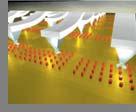
3 Molecules deposition? 500 nm JP Cleuziou, W. Wernsdorfer, V. Bouchiat, T.O., M. Monthioux, Nature Nanotech 2007 Deposited volume : towards single molecule (100 nm) 3 = 1 attoliter (10-18 l) of 1µM solution ~ 1 solute molecule Positioning on nanostructures


 BioForce")

4 Direct patterning : liquid lithography Pipettes Pins ArrayIt D. Klenermann et al., Angew. Chem. Int. Ed Ionscope Ltd BioPlume (LAAS, Toulouse) BioForce Nanosciences, Inc Ink-jet Park et al., Nature Mat. 2008
5 Dip pen nanolithography Review : Salaita et al. Nature Nanotechn Piner, R. D. Science 1999, NanoInk, Inc Massive parallelisation
 ~ 200")


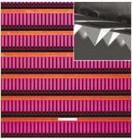
6 Methods Liquid lithography Pin and Ring method (DNA chips) ~ 200 µm Ink jet De Gan et al., Adv Mat µm Microlever plotters Belaubre et al., APL 2003 Few µm + Versatile -- Ø ~ 1 to 200 µm Dip pen lithography Piner et al., Science 1999 Hong, Mirkin, Science Ø~ 10 nm -- Limits in terms of transferrable molecules -- No reservoir


7 NADIS : liquid NAno DISpensing Meister et al, Appl. Phys. Lett A. Fang, E. Dujardin, T.O., NanoLett 2006
 2 steps : (i) Thinning")


 Smooth Si 3 N 4 surface for")
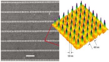
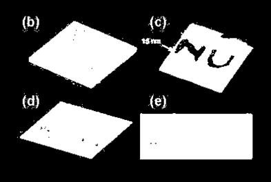
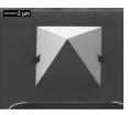
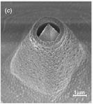
8 Fabrication of NADIS tips by focused ions beam (FIB) 2 steps : (i) Thinning of tip wall from the top (ii) milling at tip apex from tip side (record : 35 nm) nm 100 nm 100 nm 251 nm 500 nm Surface functionalization Intact smooth gold surface (for thiolate chemistry) Smooth Si 3 N 4 surface for silane chemistry

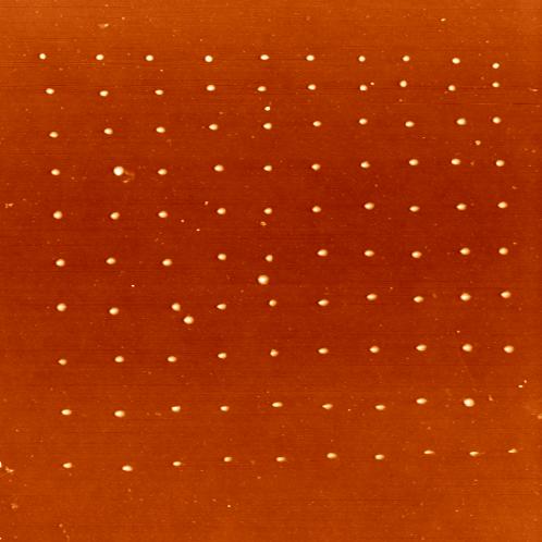
9 Deposition procedure Liquid Glycerol ou glycerol-water mixtures (dilution max 6:4) Solutions of molecules, dendrimers, proteines, nanoparticules Loading of reservoir 10µm 10µm 10µm Droplet deposited with a micropipette and micromanipulator


10 Deposition procedure AFM Multimode Picoforce in force curve mode Imaging of molecules spots Force curve
 1 µm On CF 3 -treated SiO 2 (θ")
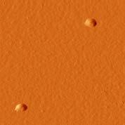
11 Influence of substrate properties Hydrophilic tip with 400 nm aperture On hydrophilic SiO 2 On NH 2 -treated SiO 2 (θ av = 53 ) 1 µm On CF 3 -treated SiO 2 (θ av = 105 )


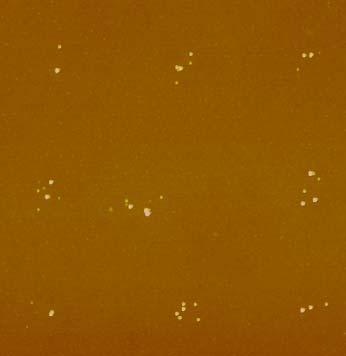
12 Ultimate dimensions : hydrophobic tips Hydrophobic tips (functionalized by dodecanethiol) 70 nm * 120 nm 35 nm Ø ~ 250 nm Ø ~ 75 nm Spot diameter ~ 2x aperture diameter 3.0µm 500nm A. Fang, E. Dujardin, T.O., NanoLett (2006)


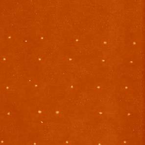
13 Intermediate sizes Mixed tips 800 nm Gold removed Ø ~ 750 nm 1,2 µm 1.0 µm Spot diameter ~ size of hydrophilic region

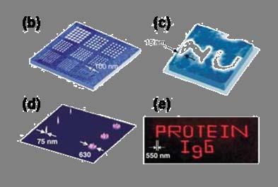
14 Patterning of nanoparticles and proteins DsRed proteins 25 nm PS NPs 250nm 1 µm 3 µm EGFP proteins 1 µm

15 Comparison with other liquid dispensing methods 1 μl 1 nl 1 pl 1 fl 1 al 1 zl 1 mm 100 μm 10 μm 1 μm 100 nm 10 nm


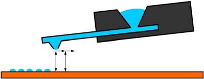
16 Deposition set-up Set-up with two AFM tips Ondarçuhu et al., Rev. Sci. Instr. 2000


17 Deposition set-up Automated deposition Nanopositioning at a predefined place 570nm 2- Droplet deposited on electrodes 1- Reference droplets 1.6µm Position accuracy : Δx, Δy ~ 100 nm 300 nm M. Ben Ali. T.O., Langmuir. 2002


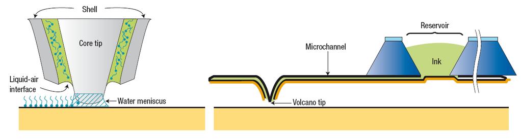
18 Limitation Evaporation of the open reservoir Cantilevers with integrated microfluidic channel Ex : NanoFountain pen Deladi et al., J. Micromech. Microengin Kim et al., Small 2005 FluidFM Meister et al., NanoLett 2009


19 Liquid transfer mechanism Flow in nanochannel Spreading on surface Spreading dynamics Capillary force


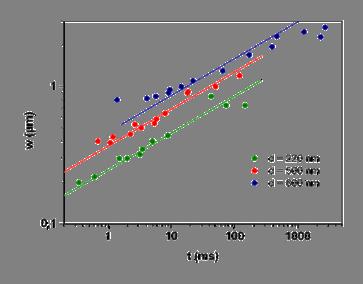
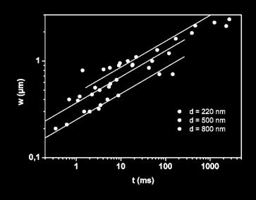
20 Writing lines 5 µm 0,25 t = w/v Dynamics of spreading at sub-micron and millisecond scales
21 Interpretation Dynamics of spreading : Cox-Voinov equation 3 3 θ = θ m + 9. Vη / γ.ln( L s ) Spreading at constant volume (θ m =0) : Tanner s law θ 1 / R 3 1 / R 9 dr dt 1/10 R t Spreading at constant pressure 10 h θ Approximations : 2 D Pressure = 0 straight interfaces θm=0 θ h R R Small angles 0 1 0,0001 0,001 0,01 0, R R 0 1 /( 3 dr R R ) 1/ 4 0 R R 0 t dt 0,1
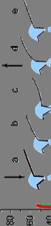
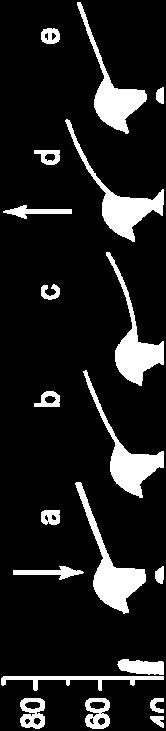

22 Real-time information Capillary force during nanodispensing
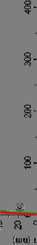
23 Interpretation of retraction force curves F (nn) z (nm) Small aperture Hydrophobic tip Hydrophilic tip Profile of retraction force curves Correlation force curve shape - drop size Liquid transfer mechanism Realtime monitoring of deposit


24 Modelization with surface evolver Energy minimization for différent boundary conditions and constraints Pressure or volume Radius or contact angle Surface shape Energy Pressure Volume Force
 0-10 -20-30 -40 z (nm) 0 20 40 60 80 100 Exp Calc Rsurf = Rtip = 37.5 nm V = 0.4 al Q Q Poiseuille Nadis 10 L. Fabié, H.")
25 Hydrophilic NADIS tips Large apertures (400 nm) Constant P defined by réservoir Small apertures (35 nm) Constant V No liquid flow during retraction F (nn) z (nm) Rsurf = 400 nm, Rtip = 300 nm P = Pa Exp Calc F (nn) z (nm) Exp Calc Rsurf = Rtip = 37.5 nm V = 0.4 al Q Q Poiseuille Nadis 10 L. Fabié, H. Durou, T.O., Langmuir, 2010 Q Q Poiseuille Nadis 0,12
 20 10")


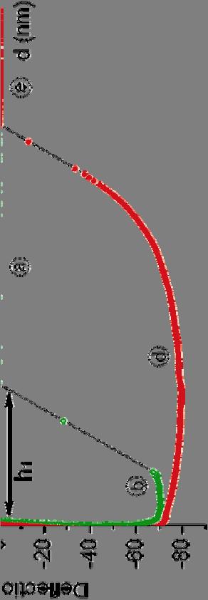
26 Correlation between droplet size and force curve Hydrophilic tip Zrupt Rsurf Rsurf F (nn) z (nm) µm 500 Z rupt (nm) Direct correlation between force curve and deposit size 100 Rtip = 250 nm R 800 surf (nm)


")


27 Evaporation of femto-droplets Mass sensing device (picogramme) J. Arcamone, et al., J.Phys.Chem B (2007) Droplet dispensing by NADIS Litterature : «microdroplets» in volume (1µl = 1 mm 3 ) This study : «femtodroplets» (1µm 3 = 1 fl) 10 9

28 Conclusion NADIS : manipulation of liquid at sub-micron scale Patterning method Towards single molecule deposition Nanopositioning on predefined structures Tool for studying liquid dynamics at sub-micron scale Spreading dynamics Nanomechanics of meniscus Evaporation of femtodroplets
Laure Fabié, Hugo Durou, Thierry Ondarçuhu Nanosciences Group, CEMES CNRS Toulouse (France)
") Nanodroplet deposition and manipulation with an AFM tip Laure Fabié, Hugo Durou, Thierry Ondarçuhu Nanosciences Group, CEMES CNRS Toulouse (France) Direct deposition methods Liquid lithography Pin and
Nanodroplet deposition and manipulation with an AFM tip Laure Fabié, Hugo Durou, Thierry Ondarçuhu Nanosciences Group, CEMES CNRS Toulouse (France) Direct deposition methods Liquid lithography Pin and
NANONICS IMAGING FOUNTAIN PEN
 NANONICS IMAGING FOUNTAIN PEN NanoLithography Systems Methods of Nanochemical Lithography Fountain Pen NanoLithography A. Lewis et al. Appl. Phys. Lett. 75, 2689 (1999) FPN controlled etching of chrome.
There's Plenty of Room at the Bottom
 There's Plenty of Room at the Bottom 12/29/1959 Feynman asked why not put the entire Encyclopedia Britannica (24 volumes) on a pin head (requires atomic scale recording). He proposed to use electron microscope
Liquid ink deposition from an atomic force microscope tip: deposition monitoring and control of feature size
 University of Wollongong Research Online Australian Institute for Innovative Materials - Papers Australian Institute for Innovative Materials 2014 Liquid ink deposition from an atomic force microscope
Nova 600 NanoLab Dual beam Focused Ion Beam IITKanpur
 Nova 600 NanoLab Dual beam Focused Ion Beam system @ IITKanpur Dual Beam Nova 600 Nano Lab From FEI company (Dual Beam = SEM + FIB) SEM: The Electron Beam for SEM Field Emission Electron Gun Energy : 500
Dip-Pen Lithography 1
 Dip-Pen Lithography 1 A Brief History of Writing Instruments From Quills and Bamboos to fountain pens and brushes M. Klein and Henry W. Wynne received US patent #68445 in 1867 for an ink chamber and delivery
Deposition of Multilayer Fibers and Beads by Near-Field Electrospinning for Texturing and 3D Printing Applications
 Deposition of Multilayer Fibers and Beads by Near-Field Electrospinning for Texturing and 3D Printing Applications Nicolas Martinez-Prieto, Jian Cao, and Kornel Ehmann Northwestern University SmartManufacturingSeries.com
The Nanotube SQUID. uhu,, M. Monthioux,, V. Bouchiat, W. Wernsdorfer, CEMES-Toulouse, CRTBT & LLN Grenoble
 The Nanotube SQUID J.-P. Cleuziou,, Th. Ondarçuhu uhu,, M. Monthioux,, V. Bouchiat, W. Wernsdorfer, CEMES-Toulouse, CRTBT & LLN Grenoble Outline Sample fabrication Proximity effect in CNT The CNT superconducting
Emerging nanopatterning
 Nanotechnology for engineers Winter semester 2006-2007 Emerging nanopatterning Soft-lithography: Microcontact printing Nanoimprint Lithography Stencil lithography Dip-Pen lithography / Nanoscale dispensing
Nano Materials. Nanomaterials
 Nano Materials 1 Contents Introduction Basics Synthesis of Nano Materials Fabrication of Nano Structure Nano Characterization Properties and Applications 2 Fabrication of Nano Structure Lithographic techniques
Liquid dispensing and writing by a nano-grooved pin
 Liquid dispensing and writing by a nano-grooved pin Hualai Dong 1,2, Xing Yang 1,2,*, Cunjing Lv 3, Quanshui Zheng 1,2,4,* 1. Department of Precision Instrument, Tsinghua University, Beijing 100084, China;
Au Ink for AFM Dip-Pen Nanolithography
 Letter Au Ink for AFM Dip-Pen Nanolithography Benjamin W. Maynor, Yan Li, and Jie Liu Langmuir, 2001, 17 (9), 2575-2578 DOI: 10.1021/la001755m Downloaded from http://pubs.acs.org on January 6, 2009 Subscriber
Electrochemically Synthesized Multi-block
 Electrochemically Synthesized Multi-block Nanorods Sungho Park SungKyunKwan University, Department of Chemistry & SKKU Advanced Institute of Nanotechnology (SAINT) J. Am. Chem. Soc. 2003, 125, 2282-2290
Self-assembled nanostructures for antireflection optical coatings
 Self-assembled nanostructures for antireflection optical coatings Yang Zhao 1, Guangzhao Mao 2, and Jinsong Wang 1 1. Deaprtment of Electrical and Computer Engineering 2. Departmentof Chemical Engineering
Diffusion modeling for Dip-pen Nanolithography Apoorv Kulkarni Graduate student, Michigan Technological University
 Diffusion modeling for Dip-pen Nanolithography Apoorv Kulkarni Graduate student, Michigan Technological University Abstract The diffusion model for the dip pen nanolithography is similar to spreading an
Fabrication at the nanoscale for nanophotonics
 Fabrication at the nanoscale for nanophotonics Ilya Sychugov, KTH Materials Physics, Kista silicon nanocrystal by electron beam induced deposition lithography Outline of basic nanofabrication methods Devices
In situ studies on dynamic properties of carbon nanotubes with metal clusters
 In situ studies on dynamic properties of carbon nanotubes with metal clusters Jason Chang, Yuan-Chih Chang, Der-Hsien Lien, Shaw-Chieh Wang*, Tung Hsu*, and Tien T. Tsong Institute of Physics, Academia
High-resolution Characterization of Organic Ultrathin Films Using Atomic Force Microscopy
 High-resolution Characterization of Organic Ultrathin Films Using Atomic Force Microscopy Jing-jiang Yu Nanotechnology Measurements Division Agilent Technologies, Inc. Atomic Force Microscopy High-Resolution
Introduction to Scanning Probe Microscopy
 WORKSHOP Nanoscience on the Tip Introduction to Scanning Probe Microscopy Table of Contents: 1 Historic Perspectives... 1 2 Scanning Force Microscopy (SFM)... 2 2.1. Contact Mode... 2 2.2. AC Mode Imaging...
Nanotechnology Fabrication Methods.
 Nanotechnology Fabrication Methods. 10 / 05 / 2016 1 Summary: 1.Introduction to Nanotechnology:...3 2.Nanotechnology Fabrication Methods:...5 2.1.Top-down Methods:...7 2.2.Bottom-up Methods:...16 3.Conclusions:...19
Lecture 3. Self-assembled Monolayers (SAM)
") 10.524 Lecture 3. Self-assembled Monolayers (SAM) Instructor: Prof. Zhiyong Gu (Chemical Engineering & UML CHN/NCOE Nanomanufacturing Center) Lecture 3: Self-assembled Monolayers (SAMs) Table of Contents
10.524 Lecture 3. Self-assembled Monolayers (SAM) Instructor: Prof. Zhiyong Gu (Chemical Engineering & UML CHN/NCOE Nanomanufacturing Center) Lecture 3: Self-assembled Monolayers (SAMs) Table of Contents
AFM Imaging In Liquids. W. Travis Johnson PhD Agilent Technologies Nanomeasurements Division
 AFM Imaging In Liquids W. Travis Johnson PhD Agilent Technologies Nanomeasurements Division Imaging Techniques: Scales Proteins 10 nm Bacteria 1μm Red Blood Cell 5μm Human Hair 75μm Si Atom Spacing 0.4nm
Outlines 3/12/2011. Vacuum Chamber. Inside the sample chamber. Nano-manipulator. Focused ion beam instrument. 1. Other components of FIB instrument
 Focused ion beam instruments Outlines 1. Other components of FIB instrument 1.a Vacuum chamber 1.b Nanomanipulator 1.c Gas supply for deposition 1.d Detectors 2. Capabilities of FIB instrument Lee Chow
Revealing High Fidelity of Nanomolding Process by Extracting the Information from AFM Image with Systematic Artifacts
 Revealing High Fidelity of Nanomolding Process by Extracting the Information from AFM Image with Systematic Artifacts Sajal Biring* Department of Electronics Engineering and Organic Electronics Research
Superhydrophobic Surfaces
 Superhydrophobic Surfaces Glen McHale and Mike Newton School of Biomedical & Natural Sciences Nottingham Trent University, UK Email: glen.mchale@ntu.ac.uk The Laboratory Themes & Expertise Wetting of surfaces
Microfluidics 2 Surface tension, contact angle, capillary flow
 MT-0.6081 Microfluidics and BioMEMS Microfluidics 2 Surface tension, contact angle, capillary flow 28.1.2017 Ville Jokinen Surface tension & Surface energy Work required to create new surface = surface
thiol monolayers by means of high-rate dynamic force spectroscopy
 1) Max Planck Institute for Polymer Research 2) Poznan University of Technology Adhesion on self-assembled thiol monolayers by means of high-rate dynamic force spectroscopy Hubert Gojżewski 1,2, Arkadiusz
Molecular dynamics study of the lifetime of nanobubbles on the substrate
 Molecular dynamics study of the lifetime of nanobubbles on the substrate - Links of Hierarchies KOHNO Shunsuke Division of Physics and Astronomy, Graduate School of Science, Kyoto University Outline Introduction
Scanning Tunneling Microscopy
 Scanning Tunneling Microscopy References: 1. G. Binnig, H. Rohrer, C. Gerber, and Weibel, Phys. Rev. Lett. 49, 57 (1982); and ibid 50, 120 (1983). 2. J. Chen, Introduction to Scanning Tunneling Microscopy,
Title Single Row Nano-Tribological Printing: A novel additive manufacturing method for nanostructures
 Nano-Tribological Printing: A novel additive manufacturing method for nanostructures H.S. Khare, N.N. Gosvami, I. Lahouij, R.W. Carpick hkhare@seas.upenn.edu carpick@seas.upenn.edu carpick.seas.upenn.edu
Bioassay on a Robust and Stretchable Extreme Wetting. Substrate through Vacuum-Based Droplet Manipulation
 Supporting Information for A Single-Droplet Multiplex Bioassay on a Robust and Stretchable Extreme Wetting Substrate through Vacuum-Based Droplet Manipulation Heetak Han, Jung Seung Lee, Hyunchul Kim,
NanoBioTechnology with DNA-nanoparticle conjugates: Nano to Bio. Bio to Nano
 JENA Electrical DNA detection and molecular nanotechnology based on DNA- conjugated metal nanoparticles Wolfgang Fritzsche Institute for Physical High Technology (IPHT) Jena NanoBioTechnology with DNA-nanoparticle
Dr. Aoife Morrin. School of Chemical Sciences Dublin City University Ireland. The National Centre for Sensor Research
 INVESTIGATION OF NANOSTRUCTURED MATERIALS FOR NOVEL BIOSENSOR FABRICATION METHODOLOGIES Dr. Aoife Morrin National Centre for Sensor Research School of Chemical Sciences Dublin City University Ireland Introduction
Supporting Information
 Supporting Information On the Minimal Size of Coffee Ring Structure Xiaoying Shen, Chih-Ming Ho and Tak-Sing Wong * Mechanical and Aerospace Engineering Department, University of California, Los Angeles,
Electrokinetic assembly and manipulation II Lecture by Chung, Jae-Hyun
 Electrokinetic assembly and manipulation II Lecture by Chung, Jae-Hyun Chung, Jae-Hyun, Mechanical Engineering, University of Washington Liu, Wing Kam, Mechanical Engineering, Northwestern University Liu,
Patterning subwavelength features by photolithography
 Arrays of Nanoscale Lenses for Subwavelength Optical Lithography pubs.acs.org/nanolett Jae-Won Jang,,,, Zijian Zheng,,,, One-Sun Lee,,, Wooyoung Shim,, Gengfeng Zheng,, George C. Schatz,*,, and Chad A.
DLVO interaction between the spheres
 DLVO interaction between the spheres DL-interaction energy for two spheres: D w ( x) 64c π ktrϕ e λ DL 2 x λ 2 0 0 D DLVO interaction w ( x) 64πkTRϕ e λ DLVO AR /12x 2 x λd 2 0 D Lecture 11 Contact angle
Supplementary Information
 Electronic Supplementary Material (ESI) for Nanoscale. This journal is The Royal Society of Chemistry 2015 Supplementary Information Visualization of equilibrium position of colloidal particles at fluid-water
Highly charged ion beams applied to fabrication of Nano-scale 3D structures. Sadao MOMOTA Kochi University of Technology
 Highly charged ion beams applied to fabrication of Nano-scale 3D structures Sadao MOMOTA Kochi University of Technology Introduction 1 Prospect of microscopic structures 2D Semiconductor 3D Ex. MEMS http://www.rise.waseda.ac.jp/proj/sci/s98s08/j-s98s08.html
Development and Characterization of High Frequency Bulk Mode Resonators
 Excerpt from the Proceedings of the COMSOL Conference 008 Hannover Development and Characterization of High Frequency Bulk Mode Resonators Hossein Pakdast 1*, Zachary James Davis 1 1 DTU Nanotech, Technical
Large-Scale and Precise Nanoparticle Placement via Electrostatic Funneling
 Large-Scale and Precise Nanoparticle Placement via Electrostatic Funneling August 21, 2007 Seong Jin Koh Materials Science and Engineering The University of Texas at Arlington Acknowledgement Vishva Ray
Biofunctionalized nanoarrays of inorganic structures prepared by dip-pen nanolithography
 INSTITUTE OF PHYSICS PUBLISHING Nanotechnology 14 (2003) 1113 1117 NANOTECHNOLOGY PII: S0957-4484(03)61790-3 Biofunctionalized nanoarrays of inorganic structures prepared by dip-pen nanolithography Hua
Lecture 7 Contact angle phenomena and wetting
 Lecture 7 Contact angle phenomena and Contact angle phenomena and wetting Young s equation Drop on the surface complete spreading Establishing finite contact angle γ cosθ = γ γ L S SL γ S γ > 0 partial
Structure-Thermal Property Correlation of Aligned Silicon. Dioxide Nanorod Arrays
 Supplementary Material for Structure-Thermal Property Correlation of Aligned Silicon Dioxide Nanorod Arrays S. Dynamic shadowing growth (DSG) technique Figure S depicts a schematic of the DSG setup. For
Nanolithography Techniques
 Nanolithography Techniques MSE 505 / MSNT 505 P. Coane Outline What Is Nanotechnology? The Motivation For Going Small Nanofabrication Technologies Basic Techniques Nano Lithography NANOTECHNOLOGY Nanotechnology
CHIMICA DELLE SUPERFICI ED INTERFASI
 CHIMICA DELLE SUPERFICI ED INTERFASI DOTT. GIULIA FIORAVANTI UNIVERSITÀ DEGLI STUDI DELL AQUILA LAUREA MAGISTRALE IN INGEGNERIA CHIMICA A.A. 2013-2014 OUTLINE SURFACE CHEMICAL GRADIENTS DROPLET MOVEMENT
High-density data storage: principle
 High-density data storage: principle Current approach High density 1 bit = many domains Information storage driven by domain wall shifts 1 bit = 1 magnetic nanoobject Single-domain needed Single easy axis
Active Plasmonic Nanostructures in Biosensing and Imaging. Bjoern M. Reinhard Department of Chemistry
 Active Plasmonic Nanostructures in Biosensing and Imaging Bjoern M. Reinhard Department of Chemistry Noble Metal Nanoparticles Light The alternating surface charges effectively form an oscillating dipole,
Elementary Process of Electromigration at Metallic Nanojunctions in the Ballistic Regime
 Elementary Process of Electromigration at Metallic Nanojunctions in the Ballistic Regime Kaz Hirakawa Institute of Industrial Science, University of Tokyo CREST, JST collaborators: Akinori Umeno, Kenji
NUMERICAL INVESTIGATION OF THERMOCAPILLARY INDUCED MOTION OF A LIQUID SLUG IN A CAPILLARY TUBE
 Proceedings of the Asian Conference on Thermal Sciences 2017, 1st ACTS March 26-30, 2017, Jeju Island, Korea ACTS-P00786 NUMERICAL INVESTIGATION OF THERMOCAPILLARY INDUCED MOTION OF A LIQUID SLUG IN A
Formation of Two-Dimensional Colloidal Sphere Arrays on Micro-Patterns
 Formation of Two-Dimensional Colloidal Sphere Arrays on Micro-Patterns Neil A. Bernotski 1, Xiaorong Xiong 2, Kerwin Wang 3, Nels E. Jewell-Larsen 4, and Karl F. Böhringer 5 Department of Electrical Engineering,
Fabrication of highly oriented microstructures and nanostructures of ferroelectric P(VDF-TrFE) copolymer via dip-pen nanolithography
 copolymer via dip-pen nanolithography") Superlattices and Microstructures 36 (2004) 21 29 www.elsevier.com/locate/superlattices Fabrication of highly oriented microstructures and nanostructures of ferroelectric P(VDF-TrFE) copolymer via dip-pen
Superlattices and Microstructures 36 (2004) 21 29 www.elsevier.com/locate/superlattices Fabrication of highly oriented microstructures and nanostructures of ferroelectric P(VDF-TrFE) copolymer via dip-pen
Presentation Phys Katia GASPERI. Statistical study of single DNA molecules into dynamic array
 Presentation Phys 730 - Katia GASPERI Statistical study of single DNA molecules into dynamic array 1 Statistical study of single DNA molecules into dynamic array - Research project lead by Laurence SALOME
Fabrication of ordered array at a nanoscopic level: context
 Fabrication of ordered array at a nanoscopic level: context Top-down method Bottom-up method Classical lithography techniques Fast processes Size limitations it ti E-beam techniques Small sizes Slow processes
Courtesy: Images on the internet
 Courtesy: Images on the internet Focus: Physics of Blowing Bubbles February 19, 2016 Physics 9, 21 Using a bubble-blowing apparatus, researchers developed a model that explains the effects of several factors,
Nanomeniscus-induced delivery of liquid solutions for diverse nanofiber fabrication
 An et al. Nano Convergence (2015) 2:13 DOI 10.1186/s40580-015-0046-6 RESEARCH Nanomeniscus-induced delivery of liquid solutions for diverse nanofiber fabrication Open Access Sangmin An 1,3, Bongsu Kim
Introduction to Micro/Nanofluidics. Date: 2015/03/13. Dr. Yi-Chung Tung. Outline
 Introduction to Micro/Nanofluidics Date: 2015/03/13 Dr. Yi-Chung Tung Outline Introduction to Microfluidics Basic Fluid Mechanics Concepts Equivalent Fluidic Circuit Model Conclusion What is Microfluidics
Nanotechnology Nanofabrication of Functional Materials. Marin Alexe Max Planck Institute of Microstructure Physics, Halle - Germany
 Nanotechnology Nanofabrication of Functional Materials Marin Alexe Max Planck Institute of Microstructure Physics, Halle - Germany Contents Part I History and background to nanotechnology Nanoworld Nanoelectronics
A study on wettability of the dual scale by plasma etch and nanohonycomb structure
 A study on wettability of the dual scale by plasma etch and nanohonycomb structure Dongseob Kim and W. Hwang* Deptment of Mechanical Engineering, Pohang University of Science and Technology, San 31, Pohang,
Supplementary Information. for
 Supplementary Information for Discrete Element Model for Suppression of Coffee-Ring Effect Ting Xu, 1 Miu Ling Lam, 2,3,4 and Ting-Hsuan Chen 1,2,3,4 1 Department of Mechanical and Biomedical Engineering,
A MEMS nanoplotter with high-density parallel dip-pen nanolithography probe arrays
 INSTITUTE OF PHYSICS PUBLISHING Nanotechnology 13 (2002) 212 217 NANOTECHNOLOGY PII: S0957-4484(02)29674-9 A MEMS nanoplotter with high-density parallel dip-pen nanolithography probe arrays Ming Zhang
E SC 412 Nanotechnology: Materials, Infrastructure, and Safety Wook Jun Nam
 E SC 412 Nanotechnology: Materials, Infrastructure, and Safety Wook Jun Nam Lecture 17 Outline Colloids and Colloidal Chemistry What is Colloids? Properties of Colloids Examples of Colloids Synthesis of
LECTURE 1 : INTRODUCTION TO NANOMECHANICS
 I LECTURE 1 : INTRODUCTION TO NANOMECHANICS Outline : NANOTECHNOLOGY / NANOMECHANICS DEFINITIONS... 2 WHY IS NANO INTERESTING?... 3 HISTORY OF NANOTECHNOLOGY/NANOMECHANICS : TIME LINE... 4 The First Talk
Presentation Phys Katia GASPERI. Statistical study of single DNA molecules into dynamic array
 Presentation Phys 730 - Katia GASPERI Statistical study of single DNA molecules into dynamic array 1 Statistical study of single DNA molecules into dynamic array - Research project lead by Laurence SALOME
Fabrication of micromachined fountain pen with in situ characterization possibility of nanoscale surface modification
 INSTITUTE OFPHYSICS PUBLISHING JOURNAL OFMICROMECHANICS ANDMICROENGINEERING J. Micromech. Microeng. 15 (2005) 528 534 doi:10.1088/0960-1317/15/3/013 Fabrication of micromachined fountain pen with in situ
Nanostructure Fabrication Using Selective Growth on Nanosize Patterns Drawn by a Scanning Probe Microscope
 Nanostructure Fabrication Using Selective Growth on Nanosize Patterns Drawn by a Scanning Probe Microscope Kentaro Sasaki, Keiji Ueno and Atsushi Koma Department of Chemistry, The University of Tokyo,
EE C247B / ME C218 INTRODUCTION TO MEMS DESIGN SPRING 2016 C. NGUYEN PROBLEM SET #4
 Issued: Wednesday, March 4, 2016 PROBLEM SET #4 Due: Monday, March 14, 2016, 8:00 a.m. in the EE C247B homework box near 125 Cory. 1. This problem considers bending of a simple cantilever and several methods
Outline Scanning Probe Microscope (SPM)
") AFM Outline Scanning Probe Microscope (SPM) A family of microscopy forms where a sharp probe is scanned across a surface and some tip/sample interactions are monitored Scanning Tunneling Microscopy (STM)
AFM Outline Scanning Probe Microscope (SPM) A family of microscopy forms where a sharp probe is scanned across a surface and some tip/sample interactions are monitored Scanning Tunneling Microscopy (STM)
Tip-Enhanced Raman Spectroscopy: Developments and Application to the study of double-stranded DNA bundles and polymer-wrapped carbon nanotubes
 Tip-Enhanced Raman Spectroscopy: Developments and Application to the study of double-stranded DNA bundles and polymer-wrapped carbon nanotubes Sébastien Bonhommeau Groupe Spectroscopie Moléculaire, ISM,
Fabrication of Resistive Random Access Memory by Atomic Force Microscope Local Anodic Oxidation
 NANO: Brief Reports and Reviews Vol. 10, No. 2 (2015) 1550028 (8 pages) World Scienti c Publishing Company DOI: 10.1142/S1793292015500289 Fabrication of Resistive Random Access Memory by Atomic Force Microscope
Lecture Topic B
 Lecture 08.11.2010 Topic B Surface Engineering Au, Cu, Ag Al2O3 HS-R (OH)3-P-O-R SiO2 X3Si-O-R Tailored Surface Chemistry Micro-contact printing Polymer stamp (PDMS) Siliconmicrostructure or PMMA resist
29: Nanotechnology. What is Nanotechnology? Properties Control and Understanding. Nanomaterials
 29: Nanotechnology What is Nanotechnology? Properties Control and Understanding Nanomaterials Making nanomaterials Seeing at the nanoscale Quantum Dots Carbon Nanotubes Biology at the Nanoscale Some Applications
Microfluidics 1 Basics, Laminar flow, shear and flow profiles
 MT-0.6081 Microfluidics and BioMEMS Microfluidics 1 Basics, Laminar flow, shear and flow profiles 11.1.2017 Ville Jokinen Outline of the next 3 weeks: Today: Microfluidics 1: Laminar flow, flow profiles,
Analysis and Measurement of Forces in an Electrowetting-Driven Oscillator
 Mater. es. Soc. Symp. Proc. Vol. 15 8 Materials esearch Society 15-DD8-1 Analysis and Measurement of Forces in an Electrowetting-Driven Oscillator Nathan Brad Crane 1, Alex A Volinsky 1, Vivek amadoss
Calculate the total volumes of the following typical microfluidic channel dimensions.
 Microfluidics and BioMEMS, 2018, Exercise 1. Unit conversions and laminar flow. (Note: this version, both the assignment and the model solutions, is now fixed (18.1.2018) so that the flow rate is 0.25µl/min
Mercury(II) detection by SERS based on a single gold microshell
 detection by SERS based on a single gold microshell") Mercury(II) detection by SERS based on a single gold microshell D. Han, S. Y. Lim, B. J. Kim, L. Piao and T. D. Chung* Department of Chemistry, Seoul National University, Seoul, Korea. 2010, 46, 5587-558
Mercury(II) detection by SERS based on a single gold microshell D. Han, S. Y. Lim, B. J. Kim, L. Piao and T. D. Chung* Department of Chemistry, Seoul National University, Seoul, Korea. 2010, 46, 5587-558
MSN551 LITHOGRAPHY II
 MSN551 Introduction to Micro and Nano Fabrication LITHOGRAPHY II E-Beam, Focused Ion Beam and Soft Lithography Why need electron beam lithography? Smaller features are required By electronics industry:
A. Optimizing the growth conditions of large-scale graphene films
 1 A. Optimizing the growth conditions of large-scale graphene films Figure S1. Optical microscope images of graphene films transferred on 300 nm SiO 2 /Si substrates. a, Images of the graphene films grown
Combinatorial Heterogeneous Catalysis
 Combinatorial Heterogeneous Catalysis 650 μm by 650 μm, spaced 100 μm apart Identification of a new blue photoluminescent (PL) composite material, Gd 3 Ga 5 O 12 /SiO 2 Science 13 March 1998: Vol. 279
Unconventional Nano-patterning. Peilin Chen
 Unconventional Nano-patterning Peilin Chen Reference Outlines History of patterning Traditional Nano-patterning Unconventional Nano-patterning Ancient Patterning "This is the Elks' land". A greeting at
MolNanoSpin: Spintronique moléculaire avec des molécules-aimants
 MolNanoSpin: Spintronique moléculaire avec des molécules-aimants W. Wernsdorfer : Institut Néel T. Mallah : Institut de Chimie Moléculaire et des Matériaux d'orsay P. Mialane : Institut Lavoisier Journées
Nanotechnology. Gavin Lawes Department of Physics and Astronomy
 Nanotechnology Gavin Lawes Department of Physics and Astronomy Earth-Moon distance 4x10 8 m (courtesy NASA) Length scales (Part I) Person 2m Magnetic nanoparticle 5x10⁻⁹ m 10 10 m 10 5 m 1 m 10-5 m 10-10
Introduction. Sample kit content
 Introduction Polymer blend sample preparation TN01062 Preparation of polymer samples available from the Lateral force, Phase imaging, and Force modulation mode kits The SBS-PMMA, SBS-PS, and SBR-PMMA samples
Title Single Row Nano-Tribological Printing: A novel additive manufacturing method for nanostructures
 Nano-Tribological Printing: A novel additive manufacturing method for nanostructures H.S. Khare, N.N. Gosvami, I. Lahouij, R.W. Carpick 1 Mechanical Engineering and Applied Mechanics, University of Pennsylvania,
Focused-ion-beam milling based nanostencil mask fabrication for spin transfer torque studies. Güntherodt
 Focused-ion-beam milling based nanostencil mask fabrication for spin transfer torque studies B. Özyilmaz a, G. Richter, N. Müsgens, M. Fraune, M. Hawraneck, B. Beschoten b, and G. Güntherodt Physikalisches
Phase Separation gives Rise to Nanoparticle Ring Formation
 Phase Separation gives Rise to Nanoparticle Ring Formation L. V. Govor, J. Parisi, and G. H. Bauer Department of Physics, University of Oldenburg, D-26111 Oldenburg, Germany Reprint requests to Dr. L.
Graphene devices and integration: A primer on challenges
 Graphene devices and integration: A primer on challenges Archana Venugopal (TI) 8 Nov 2016 Acknowledgments: Luigi Colombo (TI) UT Dallas and UT Austin 1 Outline Where we are Issues o Contact resistance
3.052 Nanomechanics of Materials and Biomaterials Thursday 02/08/06 Prof. C. Ortiz, MIT-DMSE I LECTURE 2 : THE FORCE TRANSDUCER
 I LECTURE 2 : THE FORCE TRANSDUCER Outline : LAST TIME : WHAT IS NANOMECHANICS... 2 HOW CAN WE MEASURE SUCH TINY FORCES?... 3 EXAMPLE OF A FORCE TRANSDUCER... 4 Microfabricated cantilever beams with nanosized
Diamond-like-carbon (DLC) master creation for use in soft lithography using the Atomic Force Microscope (AFM)
 master creation for use in soft lithography using the Atomic Force Microscope (AFM)") Diamond-like-carbon (DLC) master creation for use in soft lithography using the Atomic Force Microscope (AFM) Author Watson, Gregory, Myhra, S., Watson, Jolanta Published 2007 Journal Title Journal of
Diamond-like-carbon (DLC) master creation for use in soft lithography using the Atomic Force Microscope (AFM) Author Watson, Gregory, Myhra, S., Watson, Jolanta Published 2007 Journal Title Journal of
Part IV : 2-Dimensional Chiral Effect of the Organic Molecule on the Configuration of Organic Self-assembly on the Reactive Metal Surface.
 Part IV : 2-Dimensional Chiral Effect of the rganic Molecule on the Configuration of rganic Self-assembly on the eactive Metal Surface. Byung-Il Kim Department of Chemistry University of Houston Motivation
PHYSICS OF FLUID SPREADING ON ROUGH SURFACES
 INTERNATIONAL JOURNAL OF NUMERICAL ANALYSIS AND MODELING Volume 5, Supp, Pages 85 92 c 2008 Institute for Scientific Computing and Information PHYSICS OF FLUID SPREADING ON ROUGH SURFACES K. M. HAY AND
Measuring charge transport through molecules
 Measuring charge transport through molecules utline Indirect methods 1. ptical techniques 2. Electrochemical techniques Direct methods 1. Scanning probe techniques 2. In-plane electrodes 3. Break junctions
Deposition of nanoscale rhodium dots by STM assisted CVD
 J. Phys. IV France 9 (1 999) Deposition of nanoscale rhodium dots by STM assisted CVD F. Marchi, D. Tonneau, R. Pierrisnard, V. Bouchiat, V. Safarov, H. Dallaporta, P. Doppelt* and R. Even* Faculte des
PHYSICAL SELF-ASSEMBLY AND NANO-PATTERNING*
 Mater. Res. Soc. Symp. Proc. Vol. 849 2005 Materials Research Society KK8.4.1 PHYSICAL SELF-ASSEMBLY AND NANO-PATTERNING* T.-M. Lu, D.-X. Ye, T. Karabacak, and G.-C. Wang, Department of Physics, Applied
Nanoparticle Memories: CMOS, Organic and Hybrid approaches
 Nanoparticle Memories: CMOS, Organic and Hybrid approaches Panagiotis Dimitrakis, Ph.D IMEL/NCSR Demokritos Winter School on Nanoelectronic and Nanophotonics Bilkent University Ankara, Turkey 19-25 January
Microfabricated out-of-plane arrays of integrated capillary nano-electrospray emitters
 Microfabricated out-of-plane arrays of integrated capillary nano-electrospray emitters IEPC-2009-188 Presented at the 31st International Electric Propulsion Conference, University of Michigan Ann Arbor,
Nano fabrication and optical characterization of nanostructures
 Introduction to nanooptics, Summer Term 2012, Abbe School of Photonics, FSU Jena, Prof. Thomas Pertsch Nano fabrication and optical characterization of nanostructures Lecture 12 1 Optical characterization
Scanning Probe Microscopy. Amanda MacMillan, Emmy Gebremichael, & John Shamblin Chem 243: Instrumental Analysis Dr. Robert Corn March 10, 2010
 Scanning Probe Microscopy Amanda MacMillan, Emmy Gebremichael, & John Shamblin Chem 243: Instrumental Analysis Dr. Robert Corn March 10, 2010 Scanning Probe Microscopy High-Resolution Surface Analysis
Organic thin films. Robin Ras Soft Matter and Wetting group Dept. Applied Physics Aalto University.
 rganic thin films Robin Ras Soft Matter and Wetting group Dept. Applied Physics Aalto University http://physics.aalto.fi/groups/smw/ rganic thin films as stabilizer for colloids (not discussed here) solid-liquid
Enhanced Formation of a Confined Nano-Water Meniscus Using a 780 nm Laser with a Quartz Tuning Fork-Atomic Force Microscope
 Copyright 2012 American Scientific Publishers All rights reserved Printed in the United States of America Journal of Nanoscience and Nanotechnology Vol. 12, 5754 5758, 2012 Enhanced Formation of a Confined