process dependencies in nanoimprint
|
|
|
- June Matthews
- 6 years ago
- Views:
Transcription


1 Modeling and mitigating pattern and process dependencies in nanoimprint lithography 23 June 2011 Hayden Taylor Singapore-MIT Alliance for Research and Technology formerly based at: Microsystems Technology Laboratories, MIT
2 Collaborators and acknowledgements Funding MIT Singapore-MIT Alliance Duane Boning Danish National Advanced Cai Gogwilt Technology Foundation Matt Dirckx Eehern Wong NIL Technology Melinda Hale Kristian Smistrup Theodor Nielsen Helpful discussions Brian Bilenberg Hella Scheer Yoshihiko Hirai University of California, San Diego Dave White Andrew Kahng Yen-Kuan Wu 2
3 Spun-on vs droplet-dispensed resist in NIL Spun-on resist residual layer Droplet-dispensed resist time Resist viscosity 10 3 Pa.s Applied pressures ~ 5 MPa Thermoplastic or UV-curing Viscous resist squeezing Elastic stamp deflections S.Y. Chou et al., Appl. Phys. Lett. vol. 67 pp , 1995 S. Fujimori, Jpn. J. Appl. Phys. vol. 48 p. 06FH01, 2009 Resist viscosity < 0.1 Pa.s Applied pressures ~ 5 kpa Droplets tailored to pattern Key figure of merit: filling time Gas trapping and dissolution M. Colburn et al., SPIE 3676, pt.1-2, ,


4 NIL pattern and process dependencies have systematic and random components 4
5 Nanoimprinting of spun-on layers exhibits pattern dependencies Two relevant timescales for pattern formation: Local cavity filling Residual layer thickness (RLT) homogenization 5
6 We need a unified simulation approach for micro- and nano-embossing/imprinting Initial polymer thickness, r 0 10 mm 1mm Biological micro-/nano-devices stamp w r 0 polymer substrate 100 µm Tissue engineering Diffractive optics 10 µm 1 µm 100 nm Semiconductors Hard-disk drives Photovoltaics Photonics Flat-panel displays Metamaterials Planarization 1 nm 10 nm 100 nm 1 µm 10 µm 100 µm Cavity width, w Taylor, NNT
7 We need a unified simulation approach for micro- and nano-embossing/imprinting Initial polymer thickness, r 0 10 mm 1mm 100 µm 10 µm 1 µm 100 nm Biological micro-/nano-devices Tissue engineering Diffractive optics Photovoltaics Flat-panel displays Planarization Semiconductors Photonics Metamaterials Hard-disk drives Cavity 1 nm 10 nm 100 nm 1 µm 10 µm 100 µm width, w Taylor, NNT


8 Key: model impulse response g(x,y,t) of resist layer Resist Model in space: x g Mechanical impulse applied uniformly over small region at time t = 0 Resist Substrate Model in time: Newtonian: impulse response constant in time for t > 0 Viscoelastic: impulse response is function of time. Taylor, NNT After Nogi et al., Trans ASME: J Tribology, (1997) 8
9 Change in topography is given by convolution of impulse response with pressure distribution Small, unit disp. p(x,y,t) )? Stamp Resist Substrate Time increment p ( x, y, t) g( x, y, t) t 1 Pressure Impulse Unit displacement response in contact region? Taylor, NNT


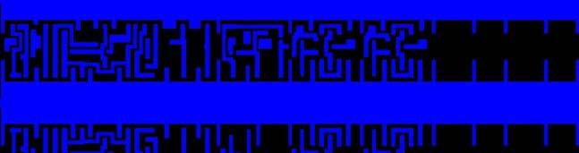
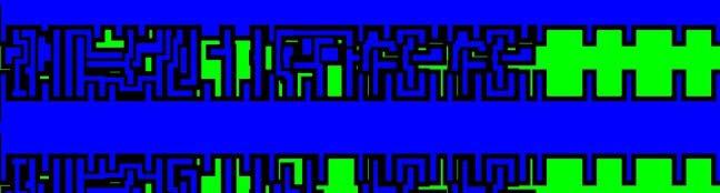
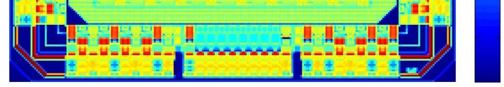
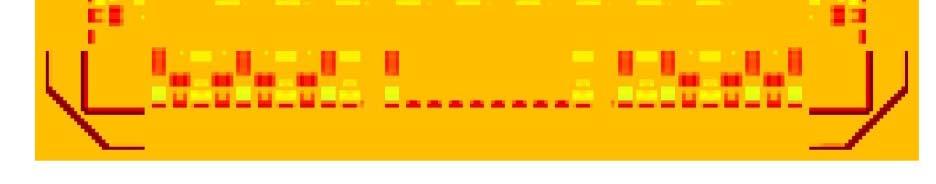
10 Contact pressure distributions can be found for arbitrary a stamp geometrieset es 2.3 µm-thick polysulfone film embossed at 205 C under 30 MPa for 2 mins Stamp design Simulated pressure Optical micrograph Cavity 200 µm MPa Taylor et al., SPIE 7269 (2009).
11 Successful modeling of polysulfone imprint 2.3 µm-thick polysulfone film embossed at 205 C under 30 MPa for 2 mins Taylor et al., SPIE 7269 (2009). 11

12 Representing layer-thickness reductions 12
13 Modeling stamp and substrate deflections Indentation Indentation and bending t stamp λ λ Magnitude of stamp deflection (log scales) ~4 λ/t stamp 13
14 Simulation method: step-up resist compliance PMMA 495K, c. 165 C, 40 MPa, 1 min Taylor, NNT
15 Abstracting a complex pattern Local relationships between pressure history and RLT: Abstractions: Stamp: pointload response Resist: impulse response HK Taylor and DS Boning, NNT 2009; SPIE 7641 (2010) Wafer: point-load response 15
,")


")
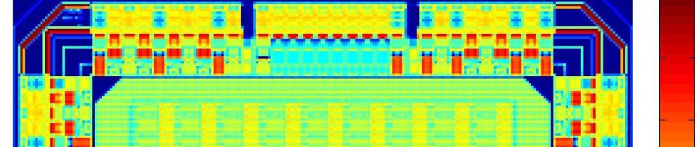
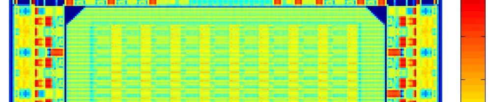
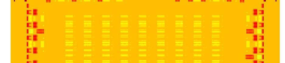
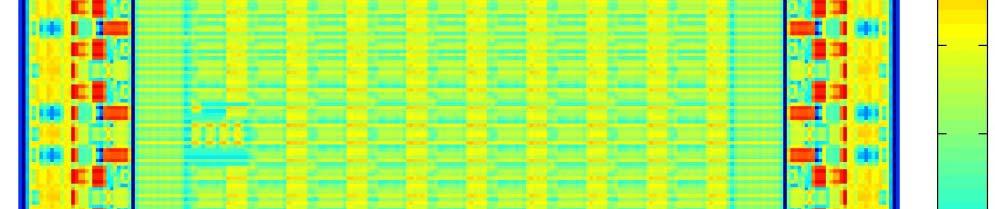
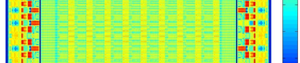
16 Our NIL simulation technique has been experimentally validated PMMA 495K (200 nm), 180 C, 10 min, 16 MPa, 10 replicates Si stamp Residu ual layer thickn ness (mi icron) cavity 0.1 protrusion 1 mm Cavity proportions filled A B C D E F G H 550 nm-deep cavities: Exp t Simulation A C E G B D F Lateral position (mm) H
 N 10 4 Expected:")


17 Simulation time Simulation time (s) N 10 4 Expected: time ~ O(N 2 logn) Stamp 1 Feature-scale Stamp 2 Simulation size, N Stamp 2 Abstracted 17
18 Strengths of the simulation method A unified simulation approach Can cope with any layer thickness Can integrate feature sizes ranging over many orders of magnitude Can model any linear viscoelastic material Speed At least 1000 times faster than feature-level FEM Implicit periodic boundary conditions are useful Realistic representation of whole-wafer wafer imprint of many chips Can use edge-padding for non-periodic modeling Suited to quick adaptation for new NIL configurations Use to explore the use of flexible stamps and substrates Explore the imprinting of non-flat substrates Micro-contact t printing; roll-to-roll 18


19 Varying stamp s bending stiffness: simulations Stamp thickness: 5 mm 0.5 mm 0.12 mm Features 200 nm 4 mm Residual layer thickness 19
20 Long-range compliance and short-range rigidity are both desirable in a TNIL stamp Long-range compliance to allow the stamp to conform to random wafer nanotopography Short-range rigidity to limit systematic pattern dependenciesd Making the stamp soft (i.e. polymeric) or thin satisfies the first aim but not the second Structuring the stamp can meet both needs 20
21 Structured stamps provide long-range compliance and short-rangerange rigidity A mechanical model of a structured stamp is needed: To ensure adequate long-range compliance while keeping fabrication affordable and maximizing the stamp area available for product features. T Nielsen, et al., Proc. 18th IEEE Conf. MEMS 2005, pp HK Taylor, K Smistrup, and DS Boning, MNE
22 Even a small flexure-gap increases wafer-scale stamp compliance several-fold HK Taylor, K Smistrup, and DS Boning, MNE

23 Simulations using a measured wafer topography illustrate long-range compliance Roughness spectra of three virgin silicon wafers HK Taylor, K Smistrup, and DS Boning, NNT
24 Simulations using a measured wafer topography illustrate long-range compliance HK Taylor, K Smistrup, and DS Boning, NNT
25 Simulations using a measured wafer topography illustrate long-range compliance Mean within- Mesa-to- mesa std. dev. (nm) mesa std. dev. (nm) Undeformed stamp topography Simulated RLTs t g = 100 µm t g = 150 µm no grooves HK Taylor, K Smistrup, and DS Boning, NNT


26 Die-scale simulations show that structuring the stamp reduces local pattern dependencies RH Pedersen, et al., J. Micromech. Microeng., vol. 18, p , HK Taylor, K Smistrup, and DS Boning, MNE
27 Structured stamps also allow for decoupling of differently patterned adjacent mesas HK Taylor, K Smistrup, and DS Boning, MNE
28 Cavity-filling time depends on length-scale of pattern-density variation, and stamp stiffness Lower-density region fills by: Lateral flow Lateral flow and stamp deflection HK Taylor, NNT
29 Cavity-filling time depends on length-scale of pattern-density variation, and stamp stiffness HK Taylor, NNT
30 If imprinted layer is an etch-mask, RLT specifications depend on resist properties (h + r max )/r max must be large enough for mask to remain intact throughout etch process Largest allowable r max r min is likely determined by lateral etch rate and critical dimension specification HK Taylor, NNT
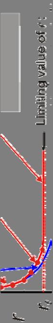
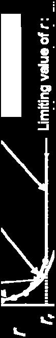
31 Time to satisfy target for RLT uniformity scales as ~W 2 for ρ above a threshold W (µm) HK Taylor, NNT


32 We postulate a cost function to drive the insertion of dummy fill into rich designs tˆ fill N 2 Wi p0 r0 h 1 0 i r0 h i 2 W i Abutting windows of size W i swept over design ρρ i is maximal density contrast between abutting windows in any location Objective is to minimize sum of contributions from N+1 window sizes h: protrusion height ht on stamp r 0 : initial resist thickness 32
33 We postulate a cost function to drive the insertion of dummy fill into rich designs insertion of dummy fill into rich designs N W N i i i fill h r h r p W t ˆ W i 2 33
34 A simple density-homogenization scheme offers faster filling and more uniform RLT Metal 1 of example integrated circuit: min. feature size 45 nm Stamp protrusion pattern density: without dummy fill Characteristic feature pitch (nm) Predominant feature orientation µm HK Taylor, NNT
35 A simple density-homogenization scheme offers faster filling and more uniform RLT Density: without fill Density: with fill Designed protrusion 1 µm Available for dummy µm 0 35
36 If stamp cavities do not fill, smaller RLTs are possible but RLT may be less uniform HK Taylor, NNT
37 Increasing keep-off distance may reduce IC parasitics, but degrades RLT performance HK Taylor, NNT


38 Summary: modeling and mitigation of process and pattern dependencies in NIL Thermal NIL Modeling Mitigating Stamp s Resist s elastic plastic deflection deformation Pattern abstraction Structured stamps: long-range compliance, short range rigidity Design rules for pattern density uniformity; dummy fill insertion Ongoing: extend to UV-NIL: Capillary pressures Gas bubble trapping Droplet spreading Mechanical proximity correction
Towards nanoimprint lithography-aware layout design checking. 25 February 2010 Hayden Taylor and Duane Boning Massachusetts Institute of Technology
 Towards nanoimprint lithography-aware layout design checking 25 February 2010 Hayden Taylor and Duane Boning Massachusetts Institute of Technology Nanoimprint is the mechanical patterning of resist spun
Outline: droplet-dispensed NIL simulation
 Defectivity prediction for droplet-dispensed UV nanoimprint lithography, enabled by fast simulation of resin flow at feature, droplet and template scales Hayden Taylor Department of Mechanical Engineering
Computationally efficient modelling of pattern dependencies in the micro-embossing of thermoplastic polymers
 Computationally efficient modelling of pattern dependencies in the micro-embossing of thermoplastic polymers Hayden Taylor and Duane Boning Microsystems Technology Laboratories Massachusetts Institute
Modeling of MEMS Fabrication Processes
 Modeling of MEMS Fabrication Processes Prof. Duane Boning Microsystems Technology Laboratories Electrical Engineering and Computer Science Massachusetts Institute of Technology September 28, 2007 Spatial
CURRENT STATUS OF NANOIMPRINT LITHOGRAPHY DEVELOPMENT IN CNMM
 U.S. -KOREA Forums on Nanotechnology 1 CURRENT STATUS OF NANOIMPRINT LITHOGRAPHY DEVELOPMENT IN CNMM February 17 th 2005 Eung-Sug Lee,Jun-Ho Jeong Korea Institute of Machinery & Materials U.S. -KOREA Forums
ALIGNMENT ACCURACY IN A MA/BA8 GEN3 USING SUBSTRATE CONFORMAL IMPRINT LITHOGRAPHY (SCIL)
") ALIGNMENT ACCURACY IN A MA/BA8 GEN3 USING SUBSTRATE CONFORMAL IMPRINT LITHOGRAPHY (SCIL) Robert Fader Fraunhofer Institute for Integrated Systems and Device Technology (IISB) Germany Ulrike Schömbs SUSS
ALIGNMENT ACCURACY IN A MA/BA8 GEN3 USING SUBSTRATE CONFORMAL IMPRINT LITHOGRAPHY (SCIL) Robert Fader Fraunhofer Institute for Integrated Systems and Device Technology (IISB) Germany Ulrike Schömbs SUSS
A modified squeeze equation for predicting the filling ratio of nanoimprint lithography
 DOI 10.1186/s40580-017-0108-z RESEARCH Open Access A modified squeeze equation for predicting the filling ratio of nanoimprint lithography JiHyeong Ryu 1, Ho Lee 1, Sang Ho Lee 2, HyungJun Lim 3,4 and
MICRO AND NANOPROCESSING TECHNOLOGIES
 LECTURE 5 MICRO AND NANOPROCESSING TECHNOLOGIES Introduction Ion lithography X-ray lithography Soft lithography E-beam lithography Concepts and processes Lithography systems Masks and resists Chapt.9.
Nanoimprint Lithography
 Nanoimprint Lithography Wei Wu Quantum Science Research Advanced Studies HP Labs, Hewlett-Packard Email: wei.wu@hp.com Outline Background Nanoimprint lithography Thermal based UV-based Applications based
Three Approaches for Nanopatterning
 Three Approaches for Nanopatterning Lithography allows the design of arbitrary pattern geometry but maybe high cost and low throughput Self-Assembly offers high throughput and low cost but limited selections
December 1999 FINAL TECHNICAL REPORT 1 Mar Mar 98
 REPORT DOCUMENTATION PAGE AFRL-SR- BL_TR " Public reporting burden for this collection of information is estimated to average 1 hour per response, including the time for reviewing instruct the collection
GHZ ELECTRICAL PROPERTIES OF CARBON NANOTUBES ON SILICON DIOXIDE MICRO BRIDGES
 GHZ ELECTRICAL PROPERTIES OF CARBON NANOTUBES ON SILICON DIOXIDE MICRO BRIDGES SHENG F. YEN 1, HAROON LAIS 1, ZHEN YU 1, SHENGDONG LI 1, WILLIAM C. TANG 1,2, AND PETER J. BURKE 1,2 1 Electrical Engineering
Technologies VII. Alternative Lithographic PROCEEDINGS OF SPIE. Douglas J. Resnick Christopher Bencher. Sponsored by. Cosponsored by.
 PROCEEDINGS OF SPIE Alternative Lithographic Technologies VII Douglas J. Resnick Christopher Bencher Editors 23-26 February 2015 San Jose, California, United States Sponsored by SPIE Cosponsored by DNS
Tool- and pattern-dependent spatial variations in silicon deep reactive ion etching
 Tool- and pattern-dependent spatial variations in silicon deep reactive ion etching Hayden Taylor Microsystems Technology Laboratories Massachusetts Institute of Technology 12 May 2006 Coping with spatial
Analytical solution for polish-rate decay in chemical mechanical polishing
 J Eng Math DOI 10.1007/s10665-010-9369-9 LETTER TO THE EDITOR Analytical solution for polish-rate decay in chemical mechanical polishing Hong Shi Terry A. Ring Received: 17 August 2009 / Accepted: 15 March
Enhanced Magnetic Properties of Bit Patterned Magnetic Recording Media by Trench-Filled Nanostructure
 CMRR Report Number 32, Summer 2009 Enhanced Magnetic Properties of Bit Patterned Magnetic Recording Media by Trench-Filled Nanostructure Edward Chulmin Choi, Daehoon Hong, Young Oh, Leon Chen, Sy-Hwang
MSN551 LITHOGRAPHY II
 MSN551 Introduction to Micro and Nano Fabrication LITHOGRAPHY II E-Beam, Focused Ion Beam and Soft Lithography Why need electron beam lithography? Smaller features are required By electronics industry:
High fidelity blazed grating replication using nanoimprint lithography
 High fidelity blazed grating replication using nanoimprint lithography Chih-Hao Chang, a) J. C. Montoya, M. Akilian, A. Lapsa, R. K. Heilmann, and M. L. Schattenburg Space Nanotechnology Laboratory, Massachusetts
Thin Wafer Handling Challenges and Emerging Solutions
 1 Thin Wafer Handling Challenges and Emerging Solutions Dr. Shari Farrens, Mr. Pete Bisson, Mr. Sumant Sood and Mr. James Hermanowski SUSS MicroTec, 228 Suss Drive, Waterbury Center, VT 05655, USA 2 Thin
EV Group. Engineered Substrates for future compound semiconductor devices
 EV Group Engineered Substrates for future compound semiconductor devices Engineered Substrates HB-LED: Engineered growth substrates GaN / GaP layer transfer Mobility enhancement solutions: III-Vs to silicon
1 INTRODUCTION 2 SAMPLE PREPARATIONS
 Chikage NORITAKE This study seeks to analyze the reliability of three-dimensional (3D) chip stacked packages under cyclic thermal loading. The critical areas of 3D chip stacked packages are defined using
Friction Drive Simulation of a SAW Motor with Slider Surface Texture Variation
 Advances in Science and Technology Vol. 54 (28) pp 366-371 online at http://www.scientific.net (28) Trans Tech Publications, Switzerland Online available since 28/Sep/2 Friction Drive Simulation of a SAW
Chemical Mechanical Planarization
 Mechanics of Contact and Lubrication, MTM G230 Department of Mechanical & Industrial Enineering Northeastern University Spring 2006 Chemical Mechanical Planarization George Calota Northeastern University
Techniken der Oberflächenphysik (Techniques of Surface Physics)
") Techniken der Oberflächenphysik (Techniques of Surface Physics) Prof. Yong Lei & Dr. Yang Xu (& Liying Liang) Fachgebiet 3D-Nanostrukturierung, Institut für Physik Contact: yong.lei@tu-ilmenau.de; yang.xu@tu-ilmenau.de;
Techniken der Oberflächenphysik (Techniques of Surface Physics) Prof. Yong Lei & Dr. Yang Xu (& Liying Liang) Fachgebiet 3D-Nanostrukturierung, Institut für Physik Contact: yong.lei@tu-ilmenau.de; yang.xu@tu-ilmenau.de;
Micro/nano and precision manufacturing technologies and applications
 The 4th China-American Frontiers of Engineering Symposium Micro/nano and precision manufacturing technologies and applications Dazhi Wang School of Mechanical Engineering Dalian University of Technology
Deformable MEMS grating for wide tunability and high operating speed
 Deformable MEMS grating for wide tunability and high operating speed Maurizio Tormen (1), Yves-Alain Peter (2), Philippe Niedermann (1), Arno Hoogerwerf (1), Herbert Shea (3) and Ross Stanley (1) 1 Centre
A. Optimizing the growth conditions of large-scale graphene films
 1 A. Optimizing the growth conditions of large-scale graphene films Figure S1. Optical microscope images of graphene films transferred on 300 nm SiO 2 /Si substrates. a, Images of the graphene films grown
A CONTACT-MECHANICS BASED MODEL FOR DISHING AND EROSION IN
 Mat. Res. Soc. Symp. Proc. Vol. 671 001 Materials Research Society A CONTACT-MECHANICS BASED MODEL FOR DISHING AND EROSION IN CHEMICAL-MECHANICAL POLISHING Joost J. Vlassak Division of Engineering and
A First Jump of Microgel; Actuation Speed Enhancement by Elastic Instability
 Electronic Supplementary Information (ESI) for A First Jump of Microgel; Actuation Speed Enhancement by Elastic Instability Howon Lee, Chunguang Xia and Nicholas X. Fang* Department of Mechanical Science
Nanostructures Fabrication Methods
 Nanostructures Fabrication Methods bottom-up methods ( atom by atom ) In the bottom-up approach, atoms, molecules and even nanoparticles themselves can be used as the building blocks for the creation of
Supplementary Figure 1 shows overall fabrication process and detailed illustrations are given
 Supplementary Figure 1. Pressure sensor fabrication schematics. Supplementary Figure 1 shows overall fabrication process and detailed illustrations are given in Methods section. (a) Firstly, the sacrificial
The Finite Element Method for Solid and Structural Mechanics
 The Finite Element Method for Solid and Structural Mechanics Sixth edition O.C. Zienkiewicz, CBE, FRS UNESCO Professor of Numerical Methods in Engineering International Centre for Numerical Methods in
MODELING OF T-SHAPED MICROCANTILEVER RESONATORS. Margarita Narducci, Eduard Figueras, Isabel Gràcia, Luis Fonseca, Joaquin Santander, Carles Cané
 Stresa, Italy, 5-7 April 007 MODELING OF T-SHAPED MICROCANTILEVER RESONATORS Margarita Narducci, Eduard Figueras, Isabel Gràcia, Luis Fonseca, Joaquin Santander, Carles Centro Nacional de Microelectrónica
Outline. 4 Mechanical Sensors Introduction General Mechanical properties Piezoresistivity Piezoresistive Sensors Capacitive sensors Applications
 Sensor devices Outline 4 Mechanical Sensors Introduction General Mechanical properties Piezoresistivity Piezoresistive Sensors Capacitive sensors Applications Introduction Two Major classes of mechanical
Supplementary Figures
 Supplementary Figures Supplementary Figure 1 Molecular structures of functional materials involved in our SGOTFT devices. Supplementary Figure 2 Capacitance measurements of a SGOTFT device. (a) Capacitance
Numerical Simulation and Experimental Study on Resist Filling Behavior in UV-nanoimprint Lithography
 Available online at www.sciencedirect.com Procedia CIRP 3 (2012 ) 203 208 45 th CIRP Conference on Manufacturing Systems 2012 Numerical Simulation and Experimental Study on Resist Filling Behavior in UV-nanoimprint
ELECTROMECHANICAL RELIABILITY TESTING OF THREE-AXIAL SILICON FORCE SENSORS
 ELECTROMECHANICAL RELIABILITY TESTING OF THREE-AXIAL SILICON FORCE SENSORS S. Spinner 1,2, J. Bartholomeyczik 1, B. Becker 2, M. Doelle 1, O. Paul 1, I. Polian 2, R. Roth 3, K. Seitz 3, and P. Ruther 1
Supplemental Material for Monolithic Multilayer Microfluidics via Sacrificial Molding of 3D- Printed Isomalt. M. K. Gelber and R.
 Electronic Supplementary Material (ESI) for Lab on a Chip. This journal is The Royal Society of Chemistry 2015 Supplemental Material for Monolithic Multilayer Microfluidics via Sacrificial Molding of 3D-
Ultrasonic Anisotropic Conductive Films (ACFs) Bonding of Flexible Substrates on Organic Rigid Boards at Room Temperature
 Bonding of Flexible Substrates on Organic Rigid Boards at Room Temperature") Ultrasonic Anisotropic Conductive Films (ACFs) Bonding of Flexible Substrates on Organic Rigid Boards at Room Temperature Kiwon Lee, Hyoung Joon Kim, Il Kim, and Kyung Wook Paik Nano Packaging and Interconnect
Ultrasonic Anisotropic Conductive Films (ACFs) Bonding of Flexible Substrates on Organic Rigid Boards at Room Temperature Kiwon Lee, Hyoung Joon Kim, Il Kim, and Kyung Wook Paik Nano Packaging and Interconnect
Impact of Modern Process Technologies on the Electrical Parameters of Interconnects
 Impact of Modern Process Technologies on the Electrical Parameters of Interconnects Debjit Sinha, Jianfeng Luo, Subramanian Rajagopalan Shabbir Batterywala, Narendra V Shenoy and Hai Zhou EECS, Northwestern
FEM-SIMULATIONS OF VIBRATIONS AND RESONANCES OF STIFF AFM CANTILEVERS
 FEM-SIMULATIONS OF VIBRATIONS AND RESONANCES OF STIFF AFM CANTILEVERS Kai GENG, Ute RABE, Sigrun HIRSEKORN Fraunhofer Institute for Nondestructive Testing (IZFP); Saarbrücken, Germany Phone: +49 681 9302
EE C247B / ME C218 INTRODUCTION TO MEMS DESIGN SPRING 2014 C. Nguyen PROBLEM SET #4
 Issued: Wednesday, Mar. 5, 2014 PROBLEM SET #4 Due (at 9 a.m.): Tuesday Mar. 18, 2014, in the EE C247B HW box near 125 Cory. 1. Suppose you would like to fabricate the suspended cross beam structure below
SENSOR DEVICES MECHANICAL SENSORS
 SENSOR DEVICES MECHANICAL SENSORS OUTLINE 4 Mechanical Sensors Introduction General mechanical properties Piezoresistivity Piezoresistive sensors Capacitive sensors Applications INTRODUCTION MECHANICAL
Emerging nanopatterning
 Nanotechnology for engineers Winter semester 2006-2007 Emerging nanopatterning Soft-lithography: Microcontact printing Nanoimprint Lithography Stencil lithography Dip-Pen lithography / Nanoscale dispensing
Nano-Lithography. Edited by Stefan Landis
 Nano-Lithography Edited by Stefan Landis IST^ m WILEY Table of Contents Foreword Jörge DE SOUSA NORONHA Introduction Michel BRILLOUET xi xvii Chapter 1. X-ray Lithography: Fundamentals and Applications
Self-study problems and questions Processing and Device Technology, FFF110/FYSD13
 Self-study problems and questions Processing and Device Technology, FFF110/FYSD13 Version 2016_01 In addition to the problems discussed at the seminars and at the lectures, you can use this set of problems
SHRINK. STACK. INTEGRATE.
 SHRINK. STACK. INTEGRATE. SUSS MICROTEC PRODUCT PORTFOLIO SHAPING THE FUTURE With more than 60 years of engineering experience SUSS MicroTec is a leading supplier of process equipment for microstructuring
Deposition of Multilayer Fibers and Beads by Near-Field Electrospinning for Texturing and 3D Printing Applications
 Deposition of Multilayer Fibers and Beads by Near-Field Electrospinning for Texturing and 3D Printing Applications Nicolas Martinez-Prieto, Jian Cao, and Kornel Ehmann Northwestern University SmartManufacturingSeries.com
High efficiency solar cells by nanophotonic design
 High efficiency solar cells by nanophotonic design Piero Spinelli Claire van Lare Jorik van de Groep Bonna Newman Mark Knight Paula Bronsveld Frank Lenzmann Ruud Schropp Wim Sinke Albert Polman Center
Control of Polymer Structures in Phase-Separated Liquid Crystal-Polymer Composite Systems
 Japanese Journal of Applied Physics Vol. 44, No. 5A, 2005, pp. 3115 3120 #2005 The Japan Society of Applied Physics Control of Polymer Structures in Phase-Separated Liquid Crystal-Polymer Composite Systems
SUPPLEMENTARY FIGURES
 SUPPLEMENTARY FIGURES a b c Supplementary Figure 1 Fabrication of the near-field radiative heat transfer device. a, Main fabrication steps for the bottom Si substrate. b, Main fabrication steps for the
56.2: Invited Paper: Pixel-Isolated Liquid Crystal Mode for Plastic Liquid Crystal Displays
 56.2: Invited Paper: Pixel-Isolated Liquid Crystal Mode for Plastic Liquid Crystal Displays Jong-Wook Jung, Se-Jin Jang, Min Young Jin, You-Jin Lee, Hak-Rin Kim, and Jae-Hoon Kim Department of Electronics
FLCC Seminar. Spacer Lithography for Reduced Variability in MOSFET Performance
 1 Seminar Spacer Lithography for Reduced Variability in MOSFET Performance Prof. Tsu-Jae King Liu Electrical Engineering & Computer Sciences Dept. University of California at Berkeley Graduate Student:
j209 7 Non-Optical Lithography
 j209 7 Non-Optical Lithography Clivia M. Sotomayor Torres and Jouni Ahopelto 7.1 Introduction In the quest to use nanofabrication methods to exploit the know-how and potentials of nanotechnology, one major
Advanced Texturing of Si Nanostructures on Low Lifetime Si Wafer
 Advanced Texturing of Si Nanostructures on Low Lifetime Si Wafer SUHAILA SEPEAI, A.W.AZHARI, SALEEM H.ZAIDI, K.SOPIAN Solar Energy Research Institute (SERI), Universiti Kebangsaan Malaysia (UKM), 43600
Proceedings MEMS Inertial Switch for Military Applications
 Proceedings MEMS Inertial Switch for Military Applications Hyo-Nam Lee 1, Seung-Gyo Jang 1, *, Sungryeol Lee 2, Jeong-Sun Lee 2 and Young-Suk Hwang 2 1 Agency for Defence Development, Daejeon, Korea; lhn4577@add.re.kr
Application of nanoindentation technique to extract properties of thin films through experimental and numerical analysis
 Materials Science-Poland, Vol. 28, No. 3, 2010 Application of nanoindentation technique to extract properties of thin films through experimental and numerical analysis A. WYMYSŁOWSKI 1*, Ł. DOWHAŃ 1, O.
Stress in Flip-Chip Solder Bumps due to Package Warpage -- Matt Pharr
 Stress in Flip-Chip Bumps due to Package Warpage -- Matt Pharr Introduction As the size of microelectronic devices continues to decrease, interconnects in the devices are scaling down correspondingly.
Technology Brief 9: Capacitive Sensors
 218 TEHNOLOGY BRIEF 9: APAITIVE SENSORS Technology Brief 9: apacitive Sensors To sense is to respond to a stimulus. (See Tech Brief 7 on resistive sensors.) A capacitor can function as a sensor if the
There's Plenty of Room at the Bottom
 There's Plenty of Room at the Bottom 12/29/1959 Feynman asked why not put the entire Encyclopedia Britannica (24 volumes) on a pin head (requires atomic scale recording). He proposed to use electron microscope
Fabrication of ordered array at a nanoscopic level: context
 Fabrication of ordered array at a nanoscopic level: context Top-down method Bottom-up method Classical lithography techniques Fast processes Size limitations it ti E-beam techniques Small sizes Slow processes
Characteristics of Thermosonic Anisotropic Conductive Adhesives (ACFs) Flip-Chip Bonding
 Flip-Chip Bonding") Materials Transactions, Vol. 51, No. 10 (2010) pp. 1790 to 1795 Special Issue on Lead-Free and Advanced Interconnection Materials for Electronics #2010 The Japan Institute of Metals Characteristics of
Materials Transactions, Vol. 51, No. 10 (2010) pp. 1790 to 1795 Special Issue on Lead-Free and Advanced Interconnection Materials for Electronics #2010 The Japan Institute of Metals Characteristics of
COMPUTATIONAL MODELING OF POLYMER FLOW IN MICROCAVITIES THROUGH A MICROSCREEN
 Proceedings of the ASME 21 International Mechanical Engineering Congress & Exposition IMECE21 November 12-18, 21, Vancouver, British Columbia, Canada IMECE21-3867 COMPUTATIONAL MODELING OF POLYMER FLOW
Mechanical Characterization of High Aspect Ratio Silicon Nanolines
 Mater. Res. Soc. Symp. Proc. Vol. 1086 2008 Materials Research Society 1086-U05-07 Mechanical Characterization of High Aspect Ratio Silicon Nanolines Bin Li 1, Huai Huang 1, Qiu Zhao 1, Zhiquan Luo 1,
MICRO-SCALE SHEET RESISTANCE MEASUREMENTS ON ULTRA SHALLOW JUNCTIONS
 MICRO-SCALE SHEET RESISTANCE MEASUREMENTS ON ULTRA SHALLOW JUNCTIONS Christian L. Petersen, Rong Lin, Dirch H. Petersen, Peter F. Nielsen CAPRES A/S, Burnaby, BC, Canada CAPRES A/S, Lyngby, Denmark We
NSC E
 NSC 892218E006071 1 Preparation of NSC Project Reports microfluidic channels are fabricated on quartz substrates and then used to imprint microstructures into Polymethylmethacrylate (PMMA) substrates using
Micro- and Nano-Technology... for Optics
 Micro- and Nano-Technology...... for Optics U.D. Zeitner Fraunhofer Institut für Angewandte Optik und Feinmechanik Jena Today: 1. Introduction E. Bernhard Kley Institute of Applied Physics Friedrich-Schiller
SEMATECH Knowledge Series 2010
 SEMATECH Knowledge Series 2010 Summary of the SEMATECH Workshop on Directed Self Assembly Lloyd Litt SEMATECH/GF Bill Hinsberg - IBM 20 October 2010 Kobe, Japan Copyright 2010 Advanced Materials Research
Improved stress prediction in adhesive bonded optical components
 Improved stress prediction in adhesive bonded optical components J. de Vreugd 1a, M.J.A. te Voert a, J.R. Nijenhuis a, J.A.C.M. Pijnenburg a, E. Tabak a a TNO optomechatronics, Stieltjesweg 1, 2628 CK,
Dynamic Strain of Ultrasonic Cu and Au Ball Bonding Measured In-Situ by Using Silicon Piezoresistive Sensor
 2017 IEEE 67th Electronic Components and Technology Conference Dynamic Strain of Ultrasonic Cu and Au Ball Bonding Measured In-Situ by Using Silicon Piezoresistive Sensor Keiichiro Iwanabe, Kenichi Nakadozono,
Nanotechnology Fabrication Methods.
 Nanotechnology Fabrication Methods. 10 / 05 / 2016 1 Summary: 1.Introduction to Nanotechnology:...3 2.Nanotechnology Fabrication Methods:...5 2.1.Top-down Methods:...7 2.2.Bottom-up Methods:...16 3.Conclusions:...19
New Die Attach Adhesives Enable Low-Stress MEMS Packaging
 New Die Attach Adhesives Enable Low-Stress MEMS Packaging Dr. Tobias Königer DELO Industrial Adhesives DELO-Allee 1; 86949 Windach; Germany Tobias.Koeniger@DELO.de Phone +49 8193 9900 365 Abstract High
Overview of the main nano-lithography techniques
 Overview of the main nano-lithography techniques Soraya Sangiao sangiao@unizar.es Outline Introduction: Nanotechnology. Nano-lithography techniques: Masked lithography techniques: Photolithography. X-ray
Highly charged ion beams applied to fabrication of Nano-scale 3D structures. Sadao MOMOTA Kochi University of Technology
 Highly charged ion beams applied to fabrication of Nano-scale 3D structures Sadao MOMOTA Kochi University of Technology Introduction 1 Prospect of microscopic structures 2D Semiconductor 3D Ex. MEMS http://www.rise.waseda.ac.jp/proj/sci/s98s08/j-s98s08.html
Design of a MEMS Capacitive Comb-drive Accelerometer
 Design of a MEMS Capacitive Comb-drive Accelerometer Tolga Kaya* 1, Behrouz Shiari 2, Kevin Petsch 1 and David Yates 2 1 Central Michigan University, 2 University of Michigan * kaya2t@cmich.edu Abstract:
MICROELECTROMECHANICAL SYSTEM (MEMS)
") IEEE SENSORS JOURNAL, VOL. 9, NO. 4, APRIL 2009 419 Analytical Model of a PZT Thick-Film Triaxial Accelerometer for Optimum Design Christian Carstensen Hindrichsen, Ninia S. Almind, Simon H. Brodersen,
IEEE SENSORS JOURNAL, VOL. 9, NO. 4, APRIL 2009 419 Analytical Model of a PZT Thick-Film Triaxial Accelerometer for Optimum Design Christian Carstensen Hindrichsen, Ninia S. Almind, Simon H. Brodersen,
Thickness Optimization of a Piezoelectric Converter for Energy Harvesting
 Excerpt from the Proceedings of the COMSOL Conference 29 Milan Thickness Optimization of a Piezoelectric Converter for Energy Harvesting M. Guizzetti* 1, V. Ferrari 1, D. Marioli 1 and T. Zawada 2 1 Dept.
ESH Benign Processes for he Integration of Quantum Dots (QDs)
") ESH Benign Processes for he Integration of Quantum Dots (QDs) PIs: Karen K. Gleason, Department of Chemical Engineering, MIT Graduate Students: Chia-Hua Lee: PhD Candidate, Department of Material Science
ESH Benign Processes for he Integration of Quantum Dots (QDs) PIs: Karen K. Gleason, Department of Chemical Engineering, MIT Graduate Students: Chia-Hua Lee: PhD Candidate, Department of Material Science
9-11 April 2008 Measurement of Large Forces and Deflections in Microstructures
 9-11 April 28 Measurement of Large Forces and Deflections in Microstructures Kai Axel Hals 1, Einar Halvorsen, and Xuyuan Chen Institute for Microsystem Technology, Vestfold University College, P.O. Box
100 nm period gratings produced by lithographically induced self-construction
 INSTITUTE OFPHYSICS PUBLISHING Nanotechnology 14 (2003) 786 790 NANOTECHNOLOGY PII: S0957-4484(03)55891-3 100 nm period gratings produced by lithographically induced self-construction Xinya Lei, Lin Wu,
Untangling the Mechanics of Entangled Biopolymers
 Untangling the Mechanics of Entangled Biopolymers Rae M. Robertson-Anderson Physics Department University of San Diego students/postdocs: Cole Chapman, PhD Tobias Falzone, PhD Stephanie Gorczyca, USD 16
Nanostrukturphysik (Nanostructure Physics)
") Nanostrukturphysik (Nanostructure Physics) Prof. Yong Lei & Dr. Yang Xu Fachgebiet 3D-Nanostrukturierung, Institut für Physik Contact: yong.lei@tu-ilmenau.de; yang.xu@tu-ilmenau.de Office: Unterpoerlitzer
Nanostrukturphysik (Nanostructure Physics) Prof. Yong Lei & Dr. Yang Xu Fachgebiet 3D-Nanostrukturierung, Institut für Physik Contact: yong.lei@tu-ilmenau.de; yang.xu@tu-ilmenau.de Office: Unterpoerlitzer
Supplementary information for
 Supplementary information for Transverse electric field dragging of DNA in a nanochannel Makusu Tsutsui, Yuhui He, Masayuki Furuhashi, Rahong Sakon, Masateru Taniguchi & Tomoji Kawai The Supplementary
D Y N A M I C M E C H A N I C A L A N A L Y S I S A N D I T S A D V A N T A G E S O V E R D E F L E C T I O N T E M P E R A T U R E U N D E R L O A D
 D Y N A M I C M E C H A N I C A L A N A L Y S I S A N D I T S A D V A N T A G E S O V E R D E F L E C T I O N T E M P E R A T U R E U N D E R L O A D Sujan E. Bin Wadud TA Instruments 9 Lukens Drive, New
Surface Acoustic Wave Linear Motor
 Proc. of 3rd Int. Heinz Nixdorf Symp., pp. 113-118, Paderborn, Germany, May, 1999 Surface Acoustic Wave Linear Motor Minoru Kuribayashi Kurosawa and Toshiro Higuchi Dept. of Precision Machinery Engineering,
DESIGN AND FABRICATION OF THE MICRO- ACCELEROMETER USING PIEZOELECTRIC THIN FILMS
 DESIGN AND FABRICATION OF THE MICRO- ACCELEROMETER USING PIEZOELECTRIC THIN FILMS JYH-CHENG YU and FU-HSIN LAI Department of Mechanical Engineering National Taiwan University of Science and Technology
Nanotechnology Nanofabrication of Functional Materials. Marin Alexe Max Planck Institute of Microstructure Physics, Halle - Germany
 Nanotechnology Nanofabrication of Functional Materials Marin Alexe Max Planck Institute of Microstructure Physics, Halle - Germany Contents Part I History and background to nanotechnology Nanoworld Nanoelectronics
Three-dimensional flexible and conductive interconnected graphene networks grown by chemical vapour deposition
 SUPPLEMENTARY INFORMATION Three-dimensional flexible and conductive interconnected graphene networks grown by chemical vapour deposition S1. Characterization of the graphene foam (GF) and GF/PDMS composites
UNLOADING OF AN ELASTIC-PLASTIC LOADED SPHERICAL CONTACT
 2004 AIMETA International Tribology Conference, September 14-17, 2004, Rome, Italy UNLOADING OF AN ELASTIC-PLASTIC LOADED SPHERICAL CONTACT Yuri KLIGERMAN( ), Yuri Kadin( ), Izhak ETSION( ) Faculty of
Slow Velocity Flow Fields in Composite Materials
 Slow Velocity Flow Fields in Composite Materials A Coupled Problem by the Homogenization Method Noboru Kikuchi and His Associates The University of Michigan Ann Arbor, MI 48109, USA Major Contributors
Notes on Rubber Friction
 Notes on Rubber Friction 2011 A G Plint Laws of Friction: In dry sliding between a given pair of materials under steady conditions, the coefficient of friction may be almost constant. This is the basis
Effect of Surface Contamination on Solid-State Bondability of Sn-Ag-Cu Bumps in Ambient Air
 Materials Transactions, Vol. 49, No. 7 (28) pp. 18 to 112 Special Issue on Lead-Free Soldering in Electronics IV #28 The Japan Institute of Metals Effect of Surface Contamination on Solid-State Bondability
1 Force Sensing. Lecture Notes. 1.1 Load Cell. 1.2 Stress and Strain
 Lecture Notes 1 Force Sensing 1.1 Load Cell A Load Cell is a structure which supports the load and deflects a known amount in response to applied forces and torques. The deflections are measured to characterize
Foundations of MEMS. Chang Liu. McCormick School of Engineering and Applied Science Northwestern University. International Edition Contributions by
 Foundations of MEMS Second Edition Chang Liu McCormick School of Engineering and Applied Science Northwestern University International Edition Contributions by Vaishali B. Mungurwadi B. V. Bhoomaraddi
Design and Simulation of A MEMS Based Horseshoe Shaped Low Current Lorentz Deformable Mirror (LCL-DM).
.") Design and Simulation of A MEMS Based Horseshoe Shaped Low Current Lorentz Deformable Mirror (LCL-DM). Byoungyoul Park 1, Tao Chen 1, Cyrus Shafai 1 1 Electrical and Computer Engineering, University of
Design and Simulation of A MEMS Based Horseshoe Shaped Low Current Lorentz Deformable Mirror (LCL-DM). Byoungyoul Park 1, Tao Chen 1, Cyrus Shafai 1 1 Electrical and Computer Engineering, University of
Chapter 2 Surface Acoustic Wave Motor Modeling and Motion Control
 Chapter 2 Surface Acoustic Wave Motor Modeling and Motion Control 1 Abstract For miniaturization of ultrasonic transducers, a surface acoustic wave device has an advantage in rigid mounting and high-power-density
Experimental research on electrical resistance of microcontacts
 Experimental research on electrical resistance of microcontacts Cristina Iliuţă, Viorel Ciornei Ştefan cel Mare University, Suceava, Romania tina_criss2005@yahoo.com Abstract: Contact resistance between
Compliant MEMS Motion Characterization by Nanoindentation
 Mater. Res. Soc. Symp. Proc. Vol. 152 28 Materials Research Society 152-DD6-24 Compliant MEMS Motion Characterization by Nanoindentation Joseph Goerges Choueifati 1, Craig Lusk 1, Xialou Pang 1,2, and
Analysis of contact deformation between a coated flat plate and a sphere and its practical application
 Computer Methods and Experimental Measurements for Surface Effects and Contact Mechanics VII 307 Analysis of contact deformation between a coated flat plate and a sphere and its practical application T.
Temporary Wafer Bonding - Key Technology for 3D-MEMS Integration
 Temporary Wafer Bonding - Key Technology for 3D-MEMS Integration 2016-06-15, Chemnitz Chemnitz University of Technology Basic Research Fraunhofer ENAS System-Packaging (SP) Back-End of Line (BEOL) Applied