Nanolithography Techniques
|
|
|
- Marianna Higgins
- 6 years ago
- Views:
Transcription
1 Nanolithography Techniques MSE 505 / MSNT 505 P. Coane
2 Outline What Is Nanotechnology? The Motivation For Going Small Nanofabrication Technologies Basic Techniques Nano Lithography
3 NANOTECHNOLOGY Nanotechnology is the design and engineering of components or structures that have at least one physical dimension the size of 100 nanometers or less. For perspective, the diameter of a human hair is roughly 100,000 nanometers. A single walled carbon nanotube has a diameter of about one nanometer. For the microelectronics industry, device structure dimensions are being reduced using top down methods scale down minimum feature size. True nanotechnology is when devices or structures are crafted by using bottom up methods i.e., by building structures up molecule by molecule.
 often display physical attributes substantially different from those displayed by either atoms or bulk")
4 Device Size (nm) Development Time Characteristic feature sizes that lie in the intermediate range between isolated atoms and bulk materials (one to 100 nanometers) often display physical attributes substantially different from those displayed by either atoms or bulk materials.
5 NANOTECHNOLOGY Motivation To Go Small To make novel devices that leverage the special properties of nanoscale building blocks consisting of a small collection of atoms. In contrast to bulk materials, having properties that are dominated by novel quantum phenomena and/or the effects of surface energy. What has been gained in the last 50 years with device shrinkage will be surpassed by the benefits of nanomaterials and their arrangement into devices. Superior selectivity for interaction, enhanced sensitivity to detection, and novel programmability for added structural and functional control (i.e. biosensors). Revolutionary new products using new materials and substances not accessible with other technologies
 (Dip Pen Nano")
6 Nanotechnology (Nano-imprint lithography) (E-beam and X-ray Nano lithography) (Dip Pen Nano lithography)
7 Nanomanufacturing Nanoassembly Techniques Layer-by-Layer Assembly Molecular Recognition-Based Self-Assembly Self-Assembled Monolayers (SAM) Nanoassembly by Step-Wise Polymerization Nanopatterning Techniques X-ray Lithography E-beam Lithography Nanoimprint Lithography Molecular Imprinting Electroless Deposition Techniques With Charged Nanoparticles Protein Nanoengineering Techniques Computer-Aided Peptide Design Automated Abiotic Peptide Synthesis Biotic Peptide Synthesis in Host Organism
8 Nanomanufacturing Not Just an Engineering Process For Atomic Scale precision and control, fundamental principles of physics and chemistry must be applied. Nanoscale Manufacturing is Multidisciplinary Involving but not limited to mechanics, electrical engineering, physics, chemistry, biology, and biomedical engineering. Nanomanufacturing is the Integration of Engineering, Science and Biology
9 Nanofabrication * Lithography In General Terms lithography can be viewed as a physical process involving image transfer or patterning into various types of media using Visible and UV Light Electron Beam Ion Beam Laser X-rays Precision Machining Printing * For Nano Fabrication A key consideration is Resolution
10 Information Flow in the Optical Lithographic Process Process Bias Every process step creates an opportunity to lose information or distort the desired pattern.
11 Optical Lithography represents the relative improvement in moving to the next generation wave length Wavelengths for optical lithography. Resolution W min uses k1 = 0.3 and DOF uses k3 = 1, assuming NA = 0.9 for all wavelengths except EUV, which assumed NA = J. Vac. Sci. Technol. B, Vol. 21, No. 6, Nov/Dec 2003
12 Optical Lithography Fundamental Limits to going below 193 nm For 157 nm - Single crystal calcium fluoride lenses required - Oxygen and water vapor absorb at this wavelength - Cost estimates are in the range of $20 million per scanner For EUV - Multi coated reflective mirrors required up to 40 layers - Reflective masks are required and must have a surface flatness of 50 nm or less from edge to edge - Mask surfaces can be damaged by oxidation. - Cost estimates are from $40 to $70 million per scanner
13 JBX-3030MV JBX-5000LS/E JBX-6000FE/E JBX-9000MV JBX-9300FS Electron Beam Systems Emitter Accelerating Voltage Min. Beam Size Beam Shape LaB6 single crystal 25 kv and 50 kv Variable LaB6 single crystal 25 kv and 50 kv 8nm Spot LaB6 single crystal 25 kv and 50 kv 5nm Spot LaB6 single crystal 50 kv Variable ZrO/W (Schottkey) 100 kv / 50 kv 4nm (100 kv) 7nm (50 kv) Spot Deflection Vector scan Vector scan Vector scan Vector scan Vector scan

14 Electron Beam Systems

15 Electron Beam Systems

16 Electron Beam Size Limits Electrons have a finite quantum mechanical wavelength: λ = 1.2 V b -1/2 Which gives a diffraction limited beam size expressed as: d d = 0.6 α λ Add all contributions to calculate theoretical minimum beam size: d d = ( d g 2 + ds 2 + dc 2 + dd 2 ) 1/2

17 Electron Beam Nanolithography 15 nm wide gold palladium lines, 50 nm periodicity, PMMA resist, fabricated by lift-off on a thin silicon nitride membrane IBM 1. RES. DEVELOP. VOL. 32 NO. 4 JULY 1988

18 Nanofabrication Electron Beam Lithography
 higher magnification view of ~10 nm lines at 30 nm period exposed at 2200 nc/cm.")

19 E-Beam Exposures in Hydrogen Silsesquioxane Resist 30 nm period grating exposed in 30-nm-thick HSQ resist on Si; (a) overall gratings, and (b) higher magnification view of ~10 nm lines at 30 nm period exposed at 2200 nc/cm. 27 nm period lines exposed in 30 nm HSQ resist on Si; (a) overall gratings and (b) higher magnification view of individual lines in the 27 nm period grating exposed at a double-pass line dose of 1650 nc/cm. J. Vac. Sci. Technol. B 21, No 6., Nov/Dec 2003
20 Nanometer Gratings by E-beam lithography Width of individual lines vs dose for 30, 40, and 50 nm periodicity gratings exposed in 30 nm of Hydrogen Silsesquioxane resist. J. Vac. Sci. Technol. B, Vol. 21, No. 6, Nov/Dec 2003
21 Nanolithography Process Window Constraints Plot of linewidth variation from nominal (i.e. developed for the time required to clear features) for up to 50% overdevelopment. Isolated features stay within a +/- 10% process window for features as small as 30 nm. Dense (line:space ratio of 1:3 or greater) features remain in the process window for features as small as 45 nm.
 Electrodeposited wire connected between electrodes.")

22 Nanofabrication Electrochemically Grown Wires for Sensor Array Applications Schematic diagram of a structure used for the electrochemical wire growth. (a) Electrodeposited wire connected between electrodes. (b) Cross-sectional view of the Si substrate, silicon nitride (1 um), Au contacts, and thermally evaporated SiO. Channels for the electrolyte solution are formed between electrodes by e-beam patterning of the SiO. Nano Lett., Vol. 4, No. 3, 2004


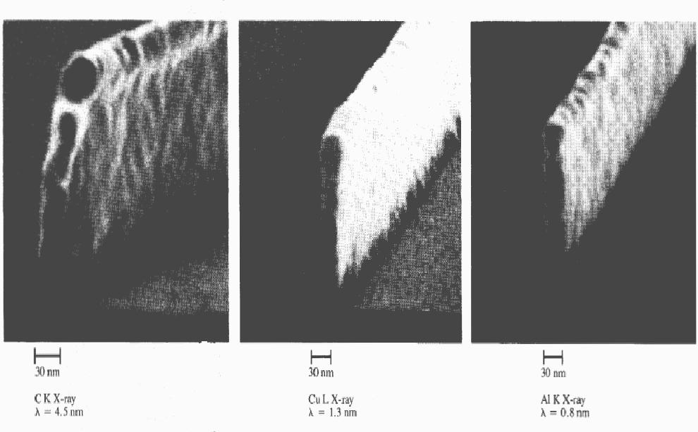
23 Nano-patterning by X-ray Lithography Scanning electron micrographs of device patterns with feature sizes less than 40 nm achieved by x-ray nanolithography followed by liftoff. The x-ray mask is shown on top and the lifted-off pattern is on the bottom.
24 X-ray Nanolithography

25 Nano-machining By using sub-nanometer control afforded by AFM technology the nm1300 employs a subtractive photomask repair technique. The current system is focused on meeting requirements for the 130- nanometer design rule node, but the technique is extendable to the 100 nm node and beyond. RAVE LLC

26 Nano-machining of MoSi on Quartz Phase Shifting Photo Mask


27 Mechanical Lithography by AFM Process sequence of mechanical AFM lithography, lift-off and pattern transfer J. Vac. Sci. Technol. B, Vol. 16, No. 5, Sep/Oct 1998
17SH). The lithography was done by applying an approximately 10X higher force during writing.")
28 Nanolithography AFM Nanografting of Thiols on a Au(111) Surface The sample is the surface of a gold crystal (Au(111)) covered with a self assembled monolayer (SAM) of decanethiol (CH3(CH2)9SH). Imaging was done under liquid in a solution containing octadecanethiol (CH3(CH2)17SH). The lithography was done by applying an approximately 10X higher force during writing. This displaced the decanethiol molecules, which were then replaced in the SAM by the longer octadecanethiol molecules. The surface is higher where written because the tails of the octadecanethiol molecules stick up above the average height of the SAM. Total size of the spirals is 620nm. Average line spacing is 40nm and average line-widths (FWHM) are 15 to 20nm. M. Liu and G. Liu, UC Davis
 is applied between the tip and the substrate.")
29 Nanolithography using Anodic Oxidation When the AFM tip is brought close to the surface, water from the ambient humidity forms a droplet between the tip and the substrate. To drive the anodic oxidation process, a voltage (5 to 15 volts) is applied between the tip and the substrate. The high electric field ionizes the water droplet and the OH- ions produced provide the oxidant for the chemical reaction.

30 Nanolithograpy Anodic Oxidation The Notre Dame logo shows 2nm thick oxide grown on a Ti film. Oxidation is performed by applying a potential to a conducting AFM tip and using the condensed water droplet at the tip as an electrochemical cell. The oxidized region grows, resulting in raised surface features. EE Department Univ. of Notre Dame

31 Nanolithography using AFM Anodic Oxidation on Ti Substrate Width at the bottom of the trench is about 80nm EE Department Univ. of Notre Dame

32 Nanolithography using AFM Anodic Oxidation - Ti Substrate The width at the top of the lines is about 70nm EE Department Univ. of Notre Dame
.")
33 Nanolithography using an STM (1) The oxide layer within the e-beam-exposed area is decomposed and reduced (2) The reduced SiO is changed to volatile SiO and evaporated from the surface at elevated temperatures. Schematic diagram of the experimental set-up for silicon oxide removal by field emitted electron beam irradiation at an elevated temperature using a Scanning Tunneling Microscope (STM). Nanotechnology 14 (2003) R55 R62


34 Nanolithography on SiO 2 using an STM Smallest linewidth = 25 nm The quantum yield for impact-induced SiO 2 decomposition as a function of the e-beam kinetic energy with beam currents of 10 na ( ), 20 na ( ), 30 na (), 40 na () and 50 na ( ). The solid curve represents the substantial yield. Nano-fabrication of patterns by PC control of the STM tip position. Nanotechnology 14 (2003) R55 R62

35 Nanofabrication on the Molecular Scale STM image of a polypropylene molecule on graphite.

36 Nanofabrication on the Molecular Scale
 molecules were connected between two gold electrodes with a nearby Al 2 O3/Al gate electrode.")
37 Nanofabrication SAM of Phenylene-Based Conjugated Molecules in an FET geometry The electronic transport characteristics of self-assembled monolayers of phenylene-based ð- conjugated molecules were measured in a three terminal device geometry. The short (1 nm) molecules were connected between two gold electrodes with a nearby Al 2 O3/Al gate electrode. It was possible to fabricate working devices using three of the five molecules investigated. The other two types of molecules led to devices where the Au electrodes were shorted together. For devices with 1,3-benzenedithiol, a weak gate effect was observed. (a) Schematic diagram of the device. The suspended bridge consists of hard baked photoresist or SiO2, and evaporated Si (or SiN). (b) Scanning-electron- microscope (SEM) image of the device that has a contact area of 400 nm2. For clarity in SEM imaging, samples were tilted 45. (c) SEM image that shows that the top surface is far away from the substrate (> 500 nm) and that the supporting middle layer features a large undercut. Thus, we can measure the transport properties of the devices without a liftoff step in the fabrication. Nano Lett., Vol. 3, No. 2, 2003

38 Nanofabrication on the Atomic Scale
39 Scanning Tunneling Microscope In the constant tunneling current mode of operation, a voltage Vz is applied to the Z piezoelectric element by means of the control unit CU to keep the tunneling current constant while the tip is scanned across the surface by altering Vx and Vy. The trace of the tip, a y-scan, generally resembles the surface topography. Electronic inhomogeneities also produce structure in the tip trace, as illustrated on the right above with two surface atoms having excessive negative charge.
 Xenon Atoms")
40 Nanopatterning on the Atomic Scale Using a Scanning Tunneling Microscope (STM) Xenon Atoms IBM 1990


41 290 nm Conducting Polymers 100 nm Protein Nanoarrays 65 nm Small Organic Molecules Silicon Nanostructures Dip-Pen Nanolithograpy 4µm Ultrahigh Density DNA Arrays Prototype Probe Arrays 1 µm Single Nanoparticle Lines 290 nm Sol Gel Structures


42 Bottom-Up Nanofabrication via Dip-Pen Nanolithograpy Building Blocks DPN-Generated Surface Templates Addressable Materials with Well-Defined Superstructures and Orientations
43 DPN: A Versatile Tool For Nanofabrication Life Sciences Microelectronics science & technology science & technology single molecule studies structure/function drug discovery ultra-high density gene chips proteomics/peptide arrays cell processes (adhesion) virus/protein crystallization (Bio)sensor Devices molecular electronics nanoscale surface phenomena organic etch resists printed nanocatalysts combinatorial materials discovery CNT, nanowire devices additive photomask repair circuit edit spintronic devices gas/chemosensors CONVERGENCE of fields from the BOTTOM UP
44 Two Fundamental Types of Dip-Pen Nanolithography Methods Direct Write write the molecule of interest directly onto the surface as the ink Templating write out an ink pattern in order to fabricate or attach something else
45 Dip-Pen Nanolithography Florida State University
46 Dip-Pen Nanolithography / SAM 16-mercaptohexadecanoic acid (MHA) Procedure for preparing functionalized DPN-generated nanostructures using thiol-containing molecules
 and dots (B), based on the DPN of MHA on a gold")
47 Dip-Pen Nanolithography / SAM AFM topographic images of the etched MHA/Au/Ti/SiOx /Si nanostructures, lines (A) and dots (B), based on the DPN of MHA on a gold surface
 and dots")
48 Dip-Pen Nanolithography / SAM AFM topographic images of individual Au nanoparticles adsorbed on HS-SAM-modified nanopatterns of lines (A, with high-resolution image inserted) and dots (B).


49 ~1.3 Million DPN Pen Array MEGApede (courtesy of NanoInk, Inc.)

50 MEGApede - DPNStamper MEGApede probe array Fluorescent arrays deposited by a MEGApede DPNStamper

51 Nanofabrication Using Self Assembly Polar Molecular Patterns Non-Polar Region Substrate Surface Functionalization SWCNT Suspension The substrate is functionalized with organic molecules to produce polar and non-polar regions. Carbon nanotubes in solution are attracted to the polar regions and selectively self assemble on the substrate following the lithographically defined patterns. SWCNT Self Assembly Mass production of carbon nanotube based circuit structures is possible

52 Imprint Lithography Fabrication sequence for three different varieties of imprint lithography.

53 Nanofabrication Using Step-and Flash Imprint Lithography 1. Using a precise piezo-driven dispense head, a silicon-rich, low-viscosity, photocurable, monomer solution is dispensed onto the substrate in the region where the pattern is to be printed. 2. The template is then pressed into contact with the wafer using very low pressures (<1psi) to spread the liquid across the field and fill the template's relief. 3. UV light is irradiated through the back of the template, curing the monomer. 4. The template, pre-coated with a fluorocarbon release agent, is removed, leaving the cured, patterned resist layer behind. 5. Finally, a breakthrough etch passing through the residual etch barrier and a transfer layer (any organic spin-coated resin such as an antireflective coating, ARC) transfers the high aspect ratio pattern to the substrate. Solid State Technology February 2004


54 Step and Flash Nano-Imprint Lithography Template pattern transfer sequence for 30 nm features. 100, 60, 30, and 20 nm features defined using the ITO-based process. J. Vac. Sci. Technol. B, Vol. 21, No. 6, Nov/Dec 2003
 Cross-sectional images of both single tier and multi-tiered features. J. Vac. Sci. Technol. B, Vol. 21, No.")
55 Step and Flash Nano-Imprint Lithography Printed features in the acrylate-based etch barrier. (a) Top-down SEMs. (b) Cross-sectional images of both single tier and multi-tiered features. J. Vac. Sci. Technol. B, Vol. 21, No. 6, Nov/Dec 2003

56 Imprint Lithography for Application to Integrated Circuit Fabrication Multi-tiered structures formed by iterating the fabrication process.
Nanotechnology Fabrication Methods.
 Nanotechnology Fabrication Methods. 10 / 05 / 2016 1 Summary: 1.Introduction to Nanotechnology:...3 2.Nanotechnology Fabrication Methods:...5 2.1.Top-down Methods:...7 2.2.Bottom-up Methods:...16 3.Conclusions:...19
MSN551 LITHOGRAPHY II
 MSN551 Introduction to Micro and Nano Fabrication LITHOGRAPHY II E-Beam, Focused Ion Beam and Soft Lithography Why need electron beam lithography? Smaller features are required By electronics industry:
Fabrication at the nanoscale for nanophotonics
 Fabrication at the nanoscale for nanophotonics Ilya Sychugov, KTH Materials Physics, Kista silicon nanocrystal by electron beam induced deposition lithography Outline of basic nanofabrication methods Devices
There's Plenty of Room at the Bottom
 There's Plenty of Room at the Bottom 12/29/1959 Feynman asked why not put the entire Encyclopedia Britannica (24 volumes) on a pin head (requires atomic scale recording). He proposed to use electron microscope
I. NANOFABRICATION O AND CHARACTERIZATION Chap. 2 : Self-Assembly
 I. Nanofabrication and Characterization : TOC I. NANOFABRICATION O AND CHARACTERIZATION Chap. 1 : Nanolithography Chap. 2 : Self-Assembly Chap. 3 : Scanning Probe Microscopy Nanoscale fabrication requirements
High-resolution Characterization of Organic Ultrathin Films Using Atomic Force Microscopy
 High-resolution Characterization of Organic Ultrathin Films Using Atomic Force Microscopy Jing-jiang Yu Nanotechnology Measurements Division Agilent Technologies, Inc. Atomic Force Microscopy High-Resolution
Fabrication of ordered array at a nanoscopic level: context
 Fabrication of ordered array at a nanoscopic level: context Top-down method Bottom-up method Classical lithography techniques Fast processes Size limitations it ti E-beam techniques Small sizes Slow processes
MEEN Nanoscale Issues in Manufacturing. Lithography Lecture 1: The Lithographic Process
 MEEN 489-500 Nanoscale Issues in Manufacturing Lithography Lecture 1: The Lithographic Process 1 Discuss Reading Assignment 1 1 Introducing Nano 2 2 Size Matters 3 3 Interlude One-The Fundamental Science
Kavli Workshop for Journalists. June 13th, CNF Cleanroom Activities
 Kavli Workshop for Journalists June 13th, 2007 CNF Cleanroom Activities Seeing nm-sized Objects with an SEM Lab experience: Scanning Electron Microscopy Equipment: Zeiss Supra 55VP Scanning electron microscopes
CURRENT STATUS OF NANOIMPRINT LITHOGRAPHY DEVELOPMENT IN CNMM
 U.S. -KOREA Forums on Nanotechnology 1 CURRENT STATUS OF NANOIMPRINT LITHOGRAPHY DEVELOPMENT IN CNMM February 17 th 2005 Eung-Sug Lee,Jun-Ho Jeong Korea Institute of Machinery & Materials U.S. -KOREA Forums
Nanotechnology. Gavin Lawes Department of Physics and Astronomy
 Nanotechnology Gavin Lawes Department of Physics and Astronomy Earth-Moon distance 4x10 8 m (courtesy NASA) Length scales (Part I) Person 2m Magnetic nanoparticle 5x10⁻⁹ m 10 10 m 10 5 m 1 m 10-5 m 10-10
Nanostructures Fabrication Methods
 Nanostructures Fabrication Methods bottom-up methods ( atom by atom ) In the bottom-up approach, atoms, molecules and even nanoparticles themselves can be used as the building blocks for the creation of
Nanoscale Issues in Materials & Manufacturing
 Nanoscale Issues in Materials & Manufacturing ENGR 213 Principles of Materials Engineering Module 2: Introduction to Nanoscale Issues Top-down and Bottom-up Approaches for Fabrication Winfried Teizer,
Three Approaches for Nanopatterning
 Three Approaches for Nanopatterning Lithography allows the design of arbitrary pattern geometry but maybe high cost and low throughput Self-Assembly offers high throughput and low cost but limited selections
Chapter 10. Nanometrology. Oxford University Press All rights reserved.
 Chapter 10 Nanometrology Oxford University Press 2013. All rights reserved. 1 Introduction Nanometrology is the science of measurement at the nanoscale level. Figure illustrates where nanoscale stands
Nanotechnology Nanofabrication of Functional Materials. Marin Alexe Max Planck Institute of Microstructure Physics, Halle - Germany
 Nanotechnology Nanofabrication of Functional Materials Marin Alexe Max Planck Institute of Microstructure Physics, Halle - Germany Contents Part I History and background to nanotechnology Nanoworld Nanoelectronics
Supplementary Figure 1 Detailed illustration on the fabrication process of templatestripped
 Supplementary Figure 1 Detailed illustration on the fabrication process of templatestripped gold substrate. (a) Spin coating of hydrogen silsesquioxane (HSQ) resist onto the silicon substrate with a thickness
Today s SPM in Nanotechnology
 Today s SPM in Nanotechnology An introduction for Advanced Applications Qun (Allen) Gu, Ph.D., AFM Scientist, Pacific Nanotechnology IEEE Bay Area Nanotechnology Council, August, 2007 8/17/2015 1 Content
MICRO AND NANOPROCESSING TECHNOLOGIES
 LECTURE 5 MICRO AND NANOPROCESSING TECHNOLOGIES Introduction Ion lithography X-ray lithography Soft lithography E-beam lithography Concepts and processes Lithography systems Masks and resists Chapt.9.
Chapter 12. Nanometrology. Oxford University Press All rights reserved.
 Chapter 12 Nanometrology Introduction Nanometrology is the science of measurement at the nanoscale level. Figure illustrates where nanoscale stands in relation to a meter and sub divisions of meter. Nanometrology
Unconventional Nano-patterning. Peilin Chen
 Unconventional Nano-patterning Peilin Chen Reference Outlines History of patterning Traditional Nano-patterning Unconventional Nano-patterning Ancient Patterning "This is the Elks' land". A greeting at
Lesson 4: Tools of the Nanosciences. Student Materials
 Lesson 4: Tools of the Nanosciences Student Materials Contents Black Box Lab Activity: Student Instructions and Worksheet Seeing and Building Small Things: Student Reading Seeing and Building Small Things:
Introduction to Scanning Probe Microscopy
 WORKSHOP Nanoscience on the Tip Introduction to Scanning Probe Microscopy Table of Contents: 1 Historic Perspectives... 1 2 Scanning Force Microscopy (SFM)... 2 2.1. Contact Mode... 2 2.2. AC Mode Imaging...
Fabrication and Domain Imaging of Iron Magnetic Nanowire Arrays
 Abstract #: 983 Program # MI+NS+TuA9 Fabrication and Domain Imaging of Iron Magnetic Nanowire Arrays D. A. Tulchinsky, M. H. Kelley, J. J. McClelland, R. Gupta, R. J. Celotta National Institute of Standards
Introduction to Photolithography
 http://www.ichaus.de/news/72 Introduction to Photolithography Photolithography The following slides present an outline of the process by which integrated circuits are made, of which photolithography is
Carbon Nanotube Thin-Films & Nanoparticle Assembly
 Nanodevices using Nanomaterials : Carbon Nanotube Thin-Films & Nanoparticle Assembly Seung-Beck Lee Division of Electronics and Computer Engineering & Department of Nanotechnology, Hanyang University,
Fabrication Methods: Chapter 4. Often two methods are typical. Top Down Bottom up. Begins with atoms or molecules. Begins with bulk materials
 Fabrication Methods: Chapter 4 Often two methods are typical Top Down Bottom up Begins with bulk materials Begins with atoms or molecules Reduced in size to nano By thermal, physical Chemical, electrochemical
29: Nanotechnology. What is Nanotechnology? Properties Control and Understanding. Nanomaterials
 29: Nanotechnology What is Nanotechnology? Properties Control and Understanding Nanomaterials Making nanomaterials Seeing at the nanoscale Quantum Dots Carbon Nanotubes Biology at the Nanoscale Some Applications
Supplementary Figure 1 a) Scheme of microfluidic device fabrication by photo and soft lithography,
 Scheme of microfluidic device fabrication by photo and soft lithography,") a b 1 mm Supplementary Figure 1 a) Scheme of microfluidic device fabrication by photo and soft lithography, (a1, a2) 50nm Pd evaporated on Si wafer with 100 nm Si 2 insulating layer and 5nm Cr as an adhesion
a b 1 mm Supplementary Figure 1 a) Scheme of microfluidic device fabrication by photo and soft lithography, (a1, a2) 50nm Pd evaporated on Si wafer with 100 nm Si 2 insulating layer and 5nm Cr as an adhesion
Techniken der Oberflächenphysik (Techniques of Surface Physics)
") Techniken der Oberflächenphysik (Techniques of Surface Physics) Prof. Yong Lei & Dr. Yang Xu (& Liying Liang) Fachgebiet 3D-Nanostrukturierung, Institut für Physik Contact: yong.lei@tu-ilmenau.de; yang.xu@tu-ilmenau.de;
Techniken der Oberflächenphysik (Techniques of Surface Physics) Prof. Yong Lei & Dr. Yang Xu (& Liying Liang) Fachgebiet 3D-Nanostrukturierung, Institut für Physik Contact: yong.lei@tu-ilmenau.de; yang.xu@tu-ilmenau.de;
Nanoimprint Lithography
 Nanoimprint Lithography Wei Wu Quantum Science Research Advanced Studies HP Labs, Hewlett-Packard Email: wei.wu@hp.com Outline Background Nanoimprint lithography Thermal based UV-based Applications based
Robust shadow-mask evaporation via lithographically controlled undercut
 Robust shadow-mask evaporation via lithographically controlled undercut B. Cord, a C. Dames, and K. K. Berggren Massachusetts Institute of Technology, Cambridge, Massachusetts 02139-4309 J. Aumentado National
Nanomaterials and their Optical Applications
 Nanomaterials and their Optical Applications Winter Semester 2013 Lecture 02 rachel.grange@uni-jena.de http://www.iap.uni-jena.de/multiphoton Lecture 2: outline 2 Introduction to Nanophotonics Theoretical
Nano Materials. Nanomaterials
 Nano Materials 1 Contents Introduction Basics Synthesis of Nano Materials Fabrication of Nano Structure Nano Characterization Properties and Applications 2 Fabrication of Nano Structure Lithographic techniques
Nova 600 NanoLab Dual beam Focused Ion Beam IITKanpur
 Nova 600 NanoLab Dual beam Focused Ion Beam system @ IITKanpur Dual Beam Nova 600 Nano Lab From FEI company (Dual Beam = SEM + FIB) SEM: The Electron Beam for SEM Field Emission Electron Gun Energy : 500
Technologies VII. Alternative Lithographic PROCEEDINGS OF SPIE. Douglas J. Resnick Christopher Bencher. Sponsored by. Cosponsored by.
 PROCEEDINGS OF SPIE Alternative Lithographic Technologies VII Douglas J. Resnick Christopher Bencher Editors 23-26 February 2015 San Jose, California, United States Sponsored by SPIE Cosponsored by DNS
Lecture 3. Self-assembled Monolayers (SAM)
") 10.524 Lecture 3. Self-assembled Monolayers (SAM) Instructor: Prof. Zhiyong Gu (Chemical Engineering & UML CHN/NCOE Nanomanufacturing Center) Lecture 3: Self-assembled Monolayers (SAMs) Table of Contents
10.524 Lecture 3. Self-assembled Monolayers (SAM) Instructor: Prof. Zhiyong Gu (Chemical Engineering & UML CHN/NCOE Nanomanufacturing Center) Lecture 3: Self-assembled Monolayers (SAMs) Table of Contents
Dip-Pen Lithography 1
 Dip-Pen Lithography 1 A Brief History of Writing Instruments From Quills and Bamboos to fountain pens and brushes M. Klein and Henry W. Wynne received US patent #68445 in 1867 for an ink chamber and delivery
Seminars in Nanosystems - I
 Seminars in Nanosystems - I Winter Semester 2011/2012 Dr. Emanuela Margapoti Emanuela.Margapoti@wsi.tum.de Dr. Gregor Koblmüller Gregor.Koblmueller@wsi.tum.de Seminar Room at ZNN 1 floor Topics of the
Measuring charge transport through molecules
 Measuring charge transport through molecules utline Indirect methods 1. ptical techniques 2. Electrochemical techniques Direct methods 1. Scanning probe techniques 2. In-plane electrodes 3. Break junctions
Lecture 14 Advanced Photolithography
 Lecture 14 Advanced Photolithography Chapter 14 Wolf and Tauber 1/74 Announcements Term Paper: You are expected to produce a 4-5 page term paper on a selected topic (from a list). Term paper contributes
SUPPLEMENTARY NOTES Supplementary Note 1: Fabrication of Scanning Thermal Microscopy Probes
 SUPPLEMENTARY NOTES Supplementary Note 1: Fabrication of Scanning Thermal Microscopy Probes Fabrication of the scanning thermal microscopy (SThM) probes is summarized in Supplementary Fig. 1 and proceeds
From nanophysics research labs to cell phones. Dr. András Halbritter Department of Physics associate professor
 From nanophysics research labs to cell phones Dr. András Halbritter Department of Physics associate professor Curriculum Vitae Birth: 1976. High-school graduation: 1994. Master degree: 1999. PhD: 2003.
Overview of the main nano-lithography techniques
 Overview of the main nano-lithography techniques Soraya Sangiao sangiao@unizar.es Outline Introduction: Nanotechnology. Nano-lithography techniques: Masked lithography techniques: Photolithography. X-ray
Crystalline Surfaces for Laser Metrology
 Crystalline Surfaces for Laser Metrology A.V. Latyshev, Institute of Semiconductor Physics SB RAS, Novosibirsk, Russia Abstract: The number of methodological recommendations has been pronounced to describe
Gold Nanoparticles Floating Gate MISFET for Non-Volatile Memory Applications
 Gold Nanoparticles Floating Gate MISFET for Non-Volatile Memory Applications D. Tsoukalas, S. Kolliopoulou, P. Dimitrakis, P. Normand Institute of Microelectronics, NCSR Demokritos, Athens, Greece S. Paul,
Nanosphere Lithography
 Nanosphere Lithography Derec Ciafre 1, Lingyun Miao 2, and Keita Oka 1 1 Institute of Optics / 2 ECE Dept. University of Rochester Abstract Nanosphere Lithography is quickly emerging as an efficient, low
.Fritjaf Capra, The Tao of Physics
 Probing inside the atom and investigating its structure, science transcended the limits of our sensory imagination. From this point on, it could no longer rely with absolute certainty on logic and common
A Novel Self-aligned and Maskless Process for Formation of Highly Uniform Arrays of Nanoholes and Nanopillars
 Nanoscale Res Lett (2008) 3: 127 DOI 10.1007/s11671-008-9124-6 NANO EXPRESS A Novel Self-aligned and Maskless Process for Formation of Highly Uniform Arrays of Nanoholes and Nanopillars Wei Wu Æ Dibyendu
In the name of Allah
 In the name of Allah Nano chemistry- 4 th stage Lecture No. 1 History of nanotechnology 16-10-2016 Assistance prof. Dr. Luma Majeed Ahmed lumamajeed2013@gmail.com, luma.ahmed@uokerbala.edu.iq Nano chemistry-4
Top down and bottom up fabrication
 Lecture 24 Top down and bottom up fabrication Lithography ( lithos stone / graphein to write) City of words lithograph h (Vito Acconci, 1999) 1930 s lithography press Photolithography d 2( NA) NA=numerical
Emerging nanopatterning
 Nanotechnology for engineers Winter semester 2006-2007 Emerging nanopatterning Soft-lithography: Microcontact printing Nanoimprint Lithography Stencil lithography Dip-Pen lithography / Nanoscale dispensing
Formation mechanism and Coulomb blockade effect in self-assembled gold quantum dots
 Formation mechanism and Coulomb blockade effect in self-assembled gold quantum dots S. F. Hu a) National Nano Device Laboratories, Hsinchu 300, Taiwan R. L. Yeh and R. S. Liu Department of Chemistry, National
Nanotechnology where size matters
 Nanotechnology where size matters J Emyr Macdonald Overview Ways of seeing very small things What is nanotechnology and why is it important? Building nanostructures What we can do with nanotechnology?
Nano Materials and Devices
 Nano Materials and Devices Professor Michael Austin Platform Technologies Research Institute Nano Materials and Devices Program Aim: to develop an integrated capability in nanotechnology Design and modelling
Instrumentation and Operation
 Instrumentation and Operation 1 STM Instrumentation COMPONENTS sharp metal tip scanning system and control electronics feedback electronics (keeps tunneling current constant) image processing system data
Title Single Row Nano-Tribological Printing: A novel additive manufacturing method for nanostructures
 Nano-Tribological Printing: A novel additive manufacturing method for nanostructures H.S. Khare, N.N. Gosvami, I. Lahouij, R.W. Carpick hkhare@seas.upenn.edu carpick@seas.upenn.edu carpick.seas.upenn.edu
Lithography Challenges Moore s Law Rising Costs and Challenges of Advanced Patterning
 Lithography Challenges Moore s Law Rising Costs and Challenges of Advanced Patterning SEMI Texas Spring Forum May 21, 2013 Austin, Texas Author / Company / Division / Rev. / Date A smartphone today has
A Novel Approach to the Layer Number-Controlled and Grain Size- Controlled Growth of High Quality Graphene for Nanoelectronics
 Supporting Information A Novel Approach to the Layer Number-Controlled and Grain Size- Controlled Growth of High Quality Graphene for Nanoelectronics Tej B. Limbu 1,2, Jean C. Hernández 3, Frank Mendoza
UNIT 3. By: Ajay Kumar Gautam Asst. Prof. Dev Bhoomi Institute of Technology & Engineering, Dehradun
 UNIT 3 By: Ajay Kumar Gautam Asst. Prof. Dev Bhoomi Institute of Technology & Engineering, Dehradun 1 Syllabus Lithography: photolithography and pattern transfer, Optical and non optical lithography, electron,
High-density data storage: principle
 High-density data storage: principle Current approach High density 1 bit = many domains Information storage driven by domain wall shifts 1 bit = 1 magnetic nanoobject Single-domain needed Single easy axis
Imaging Methods: Scanning Force Microscopy (SFM / AFM)
") Imaging Methods: Scanning Force Microscopy (SFM / AFM) The atomic force microscope (AFM) probes the surface of a sample with a sharp tip, a couple of microns long and often less than 100 Å in diameter.
Imaging Methods: Scanning Force Microscopy (SFM / AFM) The atomic force microscope (AFM) probes the surface of a sample with a sharp tip, a couple of microns long and often less than 100 Å in diameter.
Nanostructure. Materials Growth Characterization Fabrication. More see Waser, chapter 2
 Nanostructure Materials Growth Characterization Fabrication More see Waser, chapter 2 Materials growth - deposition deposition gas solid Physical Vapor Deposition Chemical Vapor Deposition Physical Vapor
Reducing dimension. Crystalline structures
 Reducing dimension 2D surfaces, interfaces and quantum wells 1D carbon nanotubes, quantum wires and conducting polymers 0D nanocrystals, nanoparticles, lithographically patterned quantum dots Crystalline
some things to think about when doing evaporation liftoff of nanometer scale patterns 1/30/09
 some things to think about when doing evaporation liftoff of nanometer scale patterns 1/30/09 review fundamentals sample sample holder r dep = deposition rate (thickness/sec) r evap = evaporation rate
Industrial Applications of Ultrafast Lasers: From Photomask Repair to Device Physics
 Industrial Applications of Ultrafast Lasers: From Photomask Repair to Device Physics Richard Haight IBM TJ Watson Research Center PO Box 218 Yorktown Hts., NY 10598 Collaborators Al Wagner Pete Longo Daeyoung
Supporting Information. Fast Synthesis of High-Performance Graphene by Rapid Thermal Chemical Vapor Deposition
 1 Supporting Information Fast Synthesis of High-Performance Graphene by Rapid Thermal Chemical Vapor Deposition Jaechul Ryu, 1,2, Youngsoo Kim, 4, Dongkwan Won, 1 Nayoung Kim, 1 Jin Sung Park, 1 Eun-Kyu
= 6 (1/ nm) So what is probability of finding electron tunneled into a barrier 3 ev high?
 So what is probability of finding electron tunneled into a barrier 3 ev high?") STM STM With a scanning tunneling microscope, images of surfaces with atomic resolution can be readily obtained. An STM uses quantum tunneling of electrons to map the density of electrons on the surface
STM STM With a scanning tunneling microscope, images of surfaces with atomic resolution can be readily obtained. An STM uses quantum tunneling of electrons to map the density of electrons on the surface
Gold nanothorns macroporous silicon hybrid structure: a simple and ultrasensitive platform for SERS
 Supporting Information Gold nanothorns macroporous silicon hybrid structure: a simple and ultrasensitive platform for SERS Kamran Khajehpour,* a Tim Williams, b,c Laure Bourgeois b,d and Sam Adeloju a
Photolithography 光刻 Part II: Photoresists
 微纳光电子材料与器件工艺原理 Photolithography 光刻 Part II: Photoresists Xing Sheng 盛兴 Department of Electronic Engineering Tsinghua University xingsheng@tsinghua.edu.cn 1 Photolithography 光刻胶 负胶 正胶 4 Photolithography
Introduction to Electron Beam Lithography
 Introduction to Electron Beam Lithography Boštjan Berčič (bostjan.bercic@ijs.si), Jožef Štefan Institute, Jamova 39, 1000 Ljubljana, Slovenia 1. Introduction Electron Beam Lithography is a specialized
Vapor-Phase Cutting of Carbon Nanotubes Using a Nanomanipulator Platform
 Vapor-Phase Cutting of Carbon Nanotubes Using a Nanomanipulator Platform MS&T 10, October 18, 2010 Vladimir Mancevski, President and CTO, Xidex Corporation Philip D. Rack, Professor, The University of
Electrochemically Synthesized Multi-block
 Electrochemically Synthesized Multi-block Nanorods Sungho Park SungKyunKwan University, Department of Chemistry & SKKU Advanced Institute of Nanotechnology (SAINT) J. Am. Chem. Soc. 2003, 125, 2282-2290
ORION NanoFab: An Overview of Applications. White Paper
 ORION NanoFab: An Overview of Applications White Paper ORION NanoFab: An Overview of Applications Author: Dr. Bipin Singh Carl Zeiss NTS, LLC, USA Date: September 2012 Introduction With the advancement
electrodeposition is a special case of electrolysis where the result is deposition of solid material on an electrode surface.
 Electrochemical Methods Electrochemical Deposition is known as electrodeposition - see CHEM* 1050 - electrolysis electrodeposition is a special case of electrolysis where the result is deposition of solid
Sub-5 nm Patterning and Applications by Nanoimprint Lithography and Helium Ion Beam Lithography
 Sub-5 nm Patterning and Applications by Nanoimprint Lithography and Helium Ion Beam Lithography Yuanrui Li 1, Ahmed Abbas 1, Yuhan Yao 1, Yifei Wang 1, Wen-Di Li 2, Chongwu Zhou 1 and Wei Wu 1* 1 Department
ESH Benign Processes for he Integration of Quantum Dots (QDs)
") ESH Benign Processes for he Integration of Quantum Dots (QDs) PIs: Karen K. Gleason, Department of Chemical Engineering, MIT Graduate Students: Chia-Hua Lee: PhD Candidate, Department of Material Science
ESH Benign Processes for he Integration of Quantum Dots (QDs) PIs: Karen K. Gleason, Department of Chemical Engineering, MIT Graduate Students: Chia-Hua Lee: PhD Candidate, Department of Material Science
Nano-Lithography. Edited by Stefan Landis
 Nano-Lithography Edited by Stefan Landis IST^ m WILEY Table of Contents Foreword Jörge DE SOUSA NORONHA Introduction Michel BRILLOUET xi xvii Chapter 1. X-ray Lithography: Fundamentals and Applications
Introduction. Photoresist : Type: Structure:
 Photoresist SEM images of the morphologies of meso structures and nanopatterns on (a) a positively nanopatterned silicon mold, and (b) a negatively nanopatterned silicon mold. Introduction Photoresist
NANOTECHNOLOGY. Students will gain an understanding of nanoscale dimensions and nanotechnology.
 NANOTECHNOLOGY By Anna M. Waldron and Carl A. Batt, Nanobiotechnology Center, Cornell University Subjects: Nanotechnology, Chemistry, Physics Time: Two class periods (approximately 90 minutes) Objective:
Supporting Information s for
 Supporting Information s for # Self-assembling of DNA-templated Au Nanoparticles into Nanowires and their enhanced SERS and Catalytic Applications Subrata Kundu* and M. Jayachandran Electrochemical Materials
Contents. What is AFM? History Basic principles and devices Operating modes Application areas Advantages and disadvantages
 Contents What is AFM? History Basic principles and devices Operating modes Application areas Advantages and disadvantages Figure1: 2004 Seth Copen Goldstein What is AFM? A type of Scanning Probe Microscopy
EE-612: Lecture 22: CMOS Process Steps
 EE-612: Lecture 22: CMOS Process Steps Mark Lundstrom Electrical and Computer Engineering Purdue University West Lafayette, IN USA Fall 2006 NCN www.nanohub.org Lundstrom EE-612 F06 1 outline 1) Unit Process
Nanostructured Materials - Fabrication Processes 1
 FABRICATION PROCESSES FOR NANOMATERIALS - NANOSTRUCTURES Lecture 6 1 Processes 1 SUBTRACTIVE AND MODIFYING METHODS Subtractive methods: Etching: wet chemical etching, reactive ion etching; ion beam sputter
Nanotechnology. Yung Liou P601 Institute of Physics Academia Sinica
 Nanotechnology Yung Liou P601 yung@phys.sinica.edu.tw Institute of Physics Academia Sinica 1 1st week Definition of Nanotechnology The Interagency Subcommittee on Nanoscale Science, Engineering and Technology
Figure 1: Some examples of objects at different size scales ( 2001, CMP Científica, [2])
![Figure 1: Some examples of objects at different size scales ( 2001, CMP Científica, [2])](/thumbs/85/91872790.jpg "Figure 1: Some examples of objects at different size scales ( 2001, CMP Científica, [2])") Top-Down vs. Bottom-Up Nanomanufacturing Prof. Derek J. Hansford, Biomedical Engineering Program and Department of Materials Science & Engineering Learning Objectives: This module should expose the student
Top-Down vs. Bottom-Up Nanomanufacturing Prof. Derek J. Hansford, Biomedical Engineering Program and Department of Materials Science & Engineering Learning Objectives: This module should expose the student
GHZ ELECTRICAL PROPERTIES OF CARBON NANOTUBES ON SILICON DIOXIDE MICRO BRIDGES
 GHZ ELECTRICAL PROPERTIES OF CARBON NANOTUBES ON SILICON DIOXIDE MICRO BRIDGES SHENG F. YEN 1, HAROON LAIS 1, ZHEN YU 1, SHENGDONG LI 1, WILLIAM C. TANG 1,2, AND PETER J. BURKE 1,2 1 Electrical Engineering
Nanostrukturphysik (Nanostructure Physics)
") Nanostrukturphysik (Nanostructure Physics) Prof. Yong Lei & Dr. Yang Xu Fachgebiet 3D-Nanostrukturierung, Institut für Physik Contact: yong.lei@tu-ilmenau.de; yang.xu@tu-ilmenau.de Office: Unterpoerlitzer
Nanostrukturphysik (Nanostructure Physics) Prof. Yong Lei & Dr. Yang Xu Fachgebiet 3D-Nanostrukturierung, Institut für Physik Contact: yong.lei@tu-ilmenau.de; yang.xu@tu-ilmenau.de Office: Unterpoerlitzer
Overview. Carbon in all its forms. Background & Discovery Fabrication. Important properties. Summary & References. Overview of current research
 Graphene Prepared for Solid State Physics II Pr Dagotto Spring 2009 Laurene Tetard 03/23/09 Overview Carbon in all its forms Background & Discovery Fabrication Important properties Overview of current
Current and Emergent Developments
 Self Assembly and Biologically Inspired Processes in Applied Nanotechnology: Current and Emergent Developments Charles Ostman VP, Electronics & Photonics Forum chair NanoSig Senior Consultant Silicon Valley
Chapter 3 : ULSI Manufacturing Technology - (c) Photolithography
 Photolithography") Chapter 3 : ULSI Manufacturing Technology - (c) Photolithography 1 Reference 1. Semiconductor Manufacturing Technology : Michael Quirk and Julian Serda (2001) 2. - (2004) 3. Semiconductor Physics and Devices-
Chapter 3 : ULSI Manufacturing Technology - (c) Photolithography 1 Reference 1. Semiconductor Manufacturing Technology : Michael Quirk and Julian Serda (2001) 2. - (2004) 3. Semiconductor Physics and Devices-
Contents. Foreword by Darrell H. Reneker
 Table of Foreword by Darrell H. Reneker Preface page xi xiii 1 Introduction 1 1.1 How big is a nanometer? 1 1.2 What is nanotechnology? 1 1.3 Historical development of nanotechnology 2 1.4 Classification
Understanding the properties and behavior of groups of interacting atoms more than simple molecules
 Condensed Matter Physics Scratching the Surface Understanding the properties and behavior of groups of interacting atoms more than simple molecules Solids and fluids in ordinary and exotic states low energy
Final Reading Assignment: Travels to the Nanoworld: pages pages pages
 Final Reading Assignment: Travels to the Nanoworld: pages 152-164 pages 201-214 pages 219-227 Bottom-up nanofabrication Can we assemble nanomachines manually? What are the components (parts)? nanoparticles
Photoresponsive Nanoscale Columnar Transistors
 Photoresponsive Nanoscale Columnar Transistors Xuefeng Guo, Shengxiong Xiao, Matthew Myers, Qian Miao, Michael L. Steigerwald, and Colin Nuckolls. Center for Nanochemistry, Beijing National Laboratory
Chapter 12 - Modern Materials
 Chapter 12 - Modern Materials 12.1 Semiconductors Inorganic compounds that semiconduct tend to have chemical formulas related to Si and Ge valence electron count of four. Semiconductor conductivity can
The goal of this project is to enhance the power density and lowtemperature efficiency of solid oxide fuel cells (SOFC) manufactured by atomic layer
 manufactured by atomic layer") Stanford University Michael Shandalov1, Shriram Ramanathan2, Changhyun Ko2 and Paul McIntyre1 1Department of Materials Science and Engineering, Stanford University 2Division of Engineering and Applied
Stanford University Michael Shandalov1, Shriram Ramanathan2, Changhyun Ko2 and Paul McIntyre1 1Department of Materials Science and Engineering, Stanford University 2Division of Engineering and Applied
Nanostructure Fabrication Using Selective Growth on Nanosize Patterns Drawn by a Scanning Probe Microscope
 Nanostructure Fabrication Using Selective Growth on Nanosize Patterns Drawn by a Scanning Probe Microscope Kentaro Sasaki, Keiji Ueno and Atsushi Koma Department of Chemistry, The University of Tokyo,
Nanophysics: Main trends
 Nano-opto-electronics Nanophysics: Main trends Nanomechanics Main issues Light interaction with small structures Molecules Nanoparticles (semiconductor and metallic) Microparticles Photonic crystals Nanoplasmonics
Institute for Electron Microscopy and Nanoanalysis Graz Centre for Electron Microscopy
 Institute for Electron Microscopy and Nanoanalysis Graz Centre for Electron Microscopy Micromechanics Ass.Prof. Priv.-Doz. DI Dr. Harald Plank a,b a Institute of Electron Microscopy and Nanoanalysis, Graz