Effect of Mechanical Stress on Gate Current and Degradation in AlGaN/GaN HEMTs
|
|
|
- Leonard Lucas Brown
- 6 years ago
- Views:
Transcription

1 Effect of Mechanical Stress on Gate Current and Degradation in AlGaN/GaN HEMTs Andrew Koehler, Min Chu, Amit Gupta, Mehmet Baykan, Scott Thompson, and Toshikazu Nishida Florida MURI Review November 10, 2011
2 Outline Motivation Stress Dependence of Gate Current and Characterization of Electric Field in AlGaN Barrier Simulation of the Dominant Stress-Altered Gate Leakage Current Gate Current Degradation under Mechanical and Electrical Stress Summary 2

 2 1 0 1")
 I G (A) ΔJ G /J G (%) 9 J G0 =")
 Time (s) 4 3 Stress (MPa) 2 1 0-1")
 t=0, As Built E V t>0,")
3 Mechanical Stress on GaN HEMT Reliability FLOORS Stress Measurements Gate Leakage Modeling Wafer Bending Stress Measurements 3 ΔR/R (%) Compression ΔR(σ) Tension Stress (MPa) I G (A) ΔJ G /J G (%) 9 J G0 = 603 x 10 3 A/m G G ΔJ G (σ) Time (s) 4 3 Stress (MPa) DFT Simulation E C E T LLO Devices V G (V) t=0, As Built E V t>0, Degradation 3

4 Gate Current Degradation Large E AlGaN Inverse PZ Mechanical Stress Defect formation Device Breakdown Increase in J G High Power State On State J. Joh, et al., IEDM 2007 (Courtesy, Erica Douglas) V DS = 0 V State Off State Systematically investigate impact of mechanical stress on J G 4
5 Outline Motivation Stress Dependence of Gate Current and Characterization of Electric Field in AlGaN Barrier Simulation of the Dominant Stress-Altered Gate Leakage Current Gate Current Degradation under Mechanical and Electrical Stress Summary 5

6 Wafer Bending (4-Point Bending) Stress on upper surface at the center of the substrate: σ E t yx a L 2a 2a 2 3 = = [Strength of Materials, edited by S. Timoshenko Krieger, Melbourne, FL,1976] E = Young s modulus t = sample thickness y = vertical displacement a, L = rod spacing t a L Neutral Axis Tension Compression Force Force y Sample 6


 Stress is")

7 GaN HEMT Wafer Bending Setup Probe tip Gold wire Conductive epoxy GaN HEMT wafer samples are too small for 4- point bending HEMT sample attached to high carbon stainless steel strip and inserted into bending setup Device is wirebonded and connected to probe tips to take electrical measurements while simultaneously applying stress Stress is calibrated using strain gauge mounted on sample (~20 MPa/graduation) Stress is applied longitudinal to channel direction GaN HEMT wafer under stress Epoxy Steel rods High carbon steel strip 7
8 J G Stress Measurement Procedure 1. Bias device in dark measuring J G V G = -0.1 to 4 V J G stable Incrementally apply stress Stress Tension Compression Incrementally release stress Avg. J G at each stress Time 8
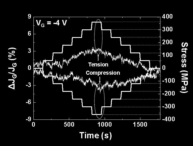


9 Experimental Results V G = V V G = -4 V 9
10 Bias and Stress Sensitivity of J G Stress sensitivity of J G decreases Characterize J G mechanism and impact of stress on J G 10
11 S Device Operation ON Condition OFF Condition AlGaN G D S AlGaN G D GaN 2DEG GaN 2DEG depleted under gate V G = 0 Ni AlGaN GaN 2DEG High reverse bias 2DEG depleted under gate Built-in field at V G = 0 2DEG is not inversion electrons (from surface states) No flatband during operation Device is turned off by depleting 2DEG V T is defined when 2DEG is depleted 11
12 Gate Leakage Transport Mechanisms ON Condition OFF Condition Ni AlGaN GaN Ni AlGaN GaN 2DEG E C 2DEG Depleted Poole-Frenkel emission Fowler-Nordheim tunneling Trap-assisted-tunneling Phonon-assisted tunneling E C To characterize gate leakage, need E AlGaN 12


 is used")


13 1D E AlGaN Calculation Ni AlGaN GaN = 1.4 ev V G = 0 = 0.4 ev E AlGaN is a function of ψ s 2DEG density (n s ) is used to calculate E AlGaN Gauss s Law E AlGaN depends on σ int and n s σ int is constant n s depends on gate voltage 13


14 Ideal Device: n s and E AlGaN n s0 No trapped charge in ideal device n s no accumulation of holes (n i ~ cm -3 ) E AlGaN V T built-in field E AlGaN saturates below V T 14
 Trapped charge")
15 Ideal vs. Actual Device Ideal device Actual Device σ int σ int No charge traps (σ int = σ PZ ) Trapped charge reduces σ int (σ int = σ PZ Q int ) Lower n s lower V T Can experimentally calculate E AlGaN 15
: σ int Integration of the C V curve C F/m 2 0.004 0.003 0.002 0.")

16 Calculating E AlGaN of Actual Device n s x10 12 n s (V G ): σ int Integration of the C V curve C F/m V T 3x x x10 12 n s (cm -2 ) Calculate n s0 Take the difference of n s0 and charge induced by gate bias V G (V) Can determine experimentally the necessary parameters for 1D E AlGaN 16
 Can experimentally calculate E AlGaN (matches 1D model)")
17 1D E AlGaN of Actual Device Q it = 0 Q it 0 Q it reduces σ int Lowers V T and E SAT Increases E AlGaN (0) Can experimentally calculate E AlGaN (matches 1D model) 17


18 Physics of E AlGaN Saturation 1D model predicts saturation of E AlGaN Verify using Sentaurus 2D simulations Self-consistently solve: Poisson s equation Electron/hole continuity equations Piezoelectricity: Piezoelectric/spontaneous polarization implemented using fixed interface charge * Used same constants as 1D calculation 18


19 Surface Potential in GaN Potential extracted 0.5 nm below AlGaN/GaN interface V G = -10 V V G = -4 V V G = -2 V V G = 0 V ψ S increases with V G at center of gate explains E AlGaN saturation Large potential drop at gate edges 19

20 2D E AlGaN Simulation at Center of Gate 2D simulated E AlGaN saturates at center of the gate Must analyze the gate edges in more detail 20


![, IEDM 2007] E AlGaN peaks at gate edge](/docs-images/77/74520191/images/21-6.jpg "could cause device breakdown (inverse")
21 E AlGaN at Gate Edge E AlGaN at 1 nm below gate contact Source Gate Drain Potential drop at gate edges results in horizontal electric-field increasing E AlGaN Gate V G = -10 V V G = -4 V V G = -2 V V G = 0 V [J. Joh, et al., IEDM 2007] E AlGaN peaks at gate edge could cause device breakdown (inverse piezoelectric effect) 21
22 Section Summary Stress sensitivity of J G decreases with increasing reverse gate bias Explained physics of E AlGaN Saturation under center of gate Peaks at gate edges Validated 1D model with experimental data and 2D simulations 22
23 Outline Motivation Stress Dependence of Gate Current and Characterization of Electric Field in AlGaN Barrier Simulation of the Dominant Stress-Altered Gate Leakage Current Gate Current Degradation under Mechanical and Electrical Stress Summary 23


![(2010)] [Sathaiya et](/docs-images/77/74520191/images/24-5.jpg "al. JAP, 99, 093701")
![(2006)] [Mitrofanov](/docs-images/77/74520191/images/24-8.jpg "et al.")
] [H Zhang")
24 Literature Review on HEMT Gate Leakage [Yan et al. APL, 97, (2010)] [Sathaiya et al. JAP, 99, (2006)] [Mitrofanov et al. JAP, 95, 6414 (2004)] [H Zhang et al. JAP, 99, (2006)] FN PFE 24
25 Direct Tunneling Formula Fowler-Nordheim Tunneling metal AlGaN GaN Thermionic Field Emission J q m m m q = E exp 8πhφb 3qhE ( / ) 8π 2 ( φ ) 3 2 * * e n 2 n b [Zhang et al. JAP, 99, (2006)] metal AlGaN GaN * qa T = k φ 0 ( ) ( ) B J f P d f FD FD φ φ φ * 1 8π 2mq 3/2 =, P= exp φ φ 3hE B φ 1+ exp kt / q [Karmalkar et al. APL, 82, 3976 (2003)]
26 Direct Tunneling Current Density Gate Current Density (A/m 2 ) 1E+5 1E-4 1E-13 Experiment TFE T = 300K m* = 0.23m e ɸ b = 1.4V Δ image lowering 1E Direct tunneling is unlikely to dominate the reverse gate leakage until at least 2.5MV/cm. FN Electric Field (MV/cm) 26 26
27 Bulk Trap-Assisted Gate Leakage 0 ɸ t ɸ B E d R1 R2 Step 1: Direct tunneling Thermal assisted tunneling Step 2: Direct tunneling Poole Frenkel emission [O Mitrofanov et al. JAP, 95, 6414 (2004)] Phonon assisted tunneling [P Pipinys et al. JAP, 99, (2006)] metal AlGaN GaN [Sathaiya et al. JAP, 99, (2006)] Assume uniform trap distribution Assume triangular potential within AlGaN Only one defect level is considered 27 27
28 Bulk Trap Leakage Model Details ( 1 ) R = C N f f P R 1 1 t FD 1 = C N f P 2 2 t 2 R1 R2 metal AlGaN GaN R: tunneling/emission rate P: tunneling/emission probability f: probability of a defect state being occupied by an electron At steady state: t FD 1 2 t 2 Cf P Cf P+ CP 1 FD 1 ( 1 ) R = R C N f f P = C N f P f = 1 FD R CC N f PP 1 1 N t FD 1 2 = = t + Cf 1 FDP1 CP 2 2 Cf 1 FDP1 CP q J = R d Ed Overall leakage current density: ( ) φ φ E φ t 28 28
29 Gate Leakage Simulation Result Gate Current Density (A/m 2 ) 1E+3 1E+2 1E+1 1E+0 1E-1 1E-2 1E-3 Experiment (E T =0.5eV) Simulation (2 nd step: FN, PFE, PAT) 1E Gate Electric Field (MV/cm) Ns = cm 3 E T = 0.82eV T = 300K The bulk trap-assisted leakage process is limited by step-1 in which electrons tunnel from metal gate to defect levels
30 Poole-Frenkel Emission from Surface States J PF I PF J PF ET ΔφT = CEexp, rkt J gate where Δ φ = β E = T πε [Yeargan et al. JAP, 39, 5600 (1968)] 3 qe AlGaN J gate J back metal AlGaN GaN J gate =J PF -J back [Harrell, et al. Thin Solid Films, 2002] α m* I back Jback = C'exp E [Yan et al. APL, 97, (2010)] I PF increases dramatically and I back is negligible once V g <
31 Poole-Frenkel Emission from Surface States 1E-5 1E-6 Symbols (experiment results) Dash lines (simulation results) 375K Log(J/E) 1E-7 1E-8 1E-9 300K r = 1.25 ± 0.06, E T = 0.49 ± 0.04 ( ) C = E (MV/cm) 1.6 1E E 1/2 0 J (A/m 2 )
32 Stress-Altered Effective Mass and Field Out of Plane m* Change (%) Effective mass change Uniaxial stress ~ 0.3% change for 400MPa -200 Biaxial stress ~ 0.5% change for 400MPa Stress (GPa) Polarization Change (%) Electric field change Uniaxial stress ~0.7% change for 400MPa -200 Biaxial stress ~1.4% change for 400MPa Stress (GPa) sp 3 d 5 tight binding model was used to simulate m out ΔE field = ΔP piezoelectric 32 32

33 Stress-Altered J G Based on Δm* and ΔE Experiment Simulation V G =-0.25V 33 33
34 Stress-Altered E T Qualitative Argument Lattice Mismatch Wafer Bending Ga N No stress Biaxial tension (2.8GPa) Uniaxial tension (0.4GPa) Uniaxial compression (0.4GPa) Θ 2 Θ 2 Θ 2 Θ 1 Θ 1 Θ 1 ΔΘ 1 <0, ΔΘ 2 >0 ΔL 1 <0, ΔL 2 >0 ΔΘ 1 <0, ΔΘ 2 >0 ΔL 1 <0, ΔL 2 >0 ΔΘ 1 >0, ΔΘ 2 <0 ΔL 1 >0, ΔL 2 <0 AlGaN AlGaN AlGaN AlGaN [Choi et al. APL vol. 92, pp (2004)] 34 34
35 Stress-Altered r-parameter No Stress Tensile Stress Compressive Stress r original Less compensation Δr > 0 Heavy compensation Δr < 0 ΔE T and Δr are treated as fitting parameters Stress affects gate leakage current mainly through ΔE T and Δr
36 Stress-Altered Gate Leakage Calculation ET ΔφT α m* Jσ = 0 = CEexp C'exp rkt E ( * +Δ *) ( ) ( ET +ΔET) Δφ α m m T Jσ 0 = C( E+ΔE) exp C'exp ( r r) kt +Δ E+ΔE ΔJG J J = J J G σ 0 σ= 0 σ =
37 Effect of Stress on J G 2.5 Simulation ΔJ / J (% / 100MPa) Fitting parameters: ΔE T = 1.6±0.3 (mev/gpa) Δr = 0.028±0.004 (/GPa) 300K 300K 375K Electric Field (MV/cm) I gate increases/decreases under uniaxial tension/compression
38 Section Summary Investigated the possible gate current mechanism of the reverse-biased GaN HEMT Determined the PFE from surface state to be the dominant leakage mechanism Simulated and understood the stress dependence of J gate. Collaborate with Erin Patrick for FLOODS gate leakage modeling 38
39 Outline Motivation Stress Dependence of Gate Current and Characterization of Electric Field in AlGaN Barrier Simulation of the Dominant Stress-Altered Gate Leakage Current Gate Current Degradation under Mechanical and Electrical Stress Summary 39


40 Theory I : AlGaN/GaN HEMT Degradation Theory II : Fresh Device Stressed Device Crystallographic defect-formation due to inverse piezoelectric effect [Dr. del Alamo s group] Metal diffusion from gate into AlGaN layer [Dr. Fan Ren s group] 40

41 Si MOS Gate Oxide Breakdown Gate: Polysilicon Conductive path I G t trace for a 1.67 nm oxide during CVS Traps Substrate [Robert O Connor et. al. Semicond. Sci. Technol. 2005] Oxide breakdown is marked by sudden increase of leakage current. Breakdown occurs due to clustering of trapped charges at localized sites, leading to enhanced conduction. Breakdown can be Soft Breakdown (SBD) or Hard Breakdown (HBD). 41

42 Time Dependent Electrical Step Stressing Vary length t of each E-stress step. Perform step stress test on GaN HEMTs, with t=10sec, 100sec, 500sec, 1000sec, and measure I G simultaneously. 42


43 Time Dependent Electrical Step Stressing Results V DS = 0V 100 sec/step Device A V G Step I G V DS = 0V 1000 sec/step Device B V G Step I G V cric = -33 V V cric = -27 V Trapping transients are observed at each stress step prior to breakdown. One large sudden increase in I G is observed, followed by multiple small jumps in I G 43


44 I G -V G after Electrical Step Stressing Device A Device B After stress test V DS =0V After stress test V DS =0V Before stress test Before stress test Increase in I G is observed after device degradation 44


45 Combined Electrical and Mechanical Stressing Measure I G during the application of stress Need to determine step size for E-stress and mechanical stress 45
 S = Strain matrix (6X1) E = Field (3X1) c E = stiffness matrix (6X6) s E = compliance matrix (6X6) d t,e t = piezoelectric matrix (3X6) V G (V) 0-4")
46 Piezoelectric Constitutive Relation T S = = c s t E. S e. E t E. T + d. E T= Stress matrix (6X1) S = Strain matrix (6X1) E = Field (3X1) c E = stiffness matrix (6X6) s E = compliance matrix (6X6) d t,e t = piezoelectric matrix (3X6) V G (V) V GS =-2V V GS =-1V -1V of V G generates ~10 MPa of biaxial tensile stress 46


47 Experimental Set Up E-Stress Mechanical Stress Courtesy, David Cheney V G step size is -5V, each applied for 8min Uniaxial mechanical stress is applied in steps of 15 MPa, upto 150 MPa max. 47


48 I G Degradation under Electrical-Mechanical stress Breakdown point: V G = -25V σ = 60 MPa E-Stress Mechanical Stress I G 48
49 Section Summary Measured I G under E stress stepping at varying lengths of stress step Device Flow: AFRL E-stress Mechanical Stress for t>0 Integrated mechanical stress and electrical stress to perform degradation experiments 49
50 Summary and Future Work Investigated the dominant leakage mechanism to be PFE in reverse-biased AlGaN/GaN HEMT Stress sensitivity of gate current decreases with increasing reverse bias Determined that inverse piezoelectric effect plays significant role in AlGaN/GaN HEMT failure Device Flow: AFRL E Stress Mechanical Stress (next to LEAP) Theory Flow: Stress dependent gate leakage modeling Electromechanical (FLOORS) 50
51 Acknowledgments MURI FUNDING 51
52 Effect of Mechanical Stress on Gate Current and Degradation in AlGaN/GaN HEMTs QUESTIONS? 52
Recent Progress in Understanding the DC and RF Reliability of GaN High Electron Mobility Transistors
 Recent Progress in Understanding the DC and RF Reliability of GaN High Electron Mobility Transistors J. A. del Alamo and J. Joh* Microsystems Technology Laboratories, MIT, Cambridge, MA *Presently with
Role of Electrochemical Reactions in the Degradation Mechanisms of AlGaN/GaN HEMTs
 Role of Electrochemical Reactions in the Degradation Mechanisms of AlGaN/GaN HEMTs Feng Gao 1,2, Bin Lu 2, Carl V. Thompson 1, Jesús del Alamo 2, Tomás Palacios 2 1. Department of Materials Science and
IMPACT OF MECHANICAL STRESS ON ALGAN/GAN HEMT PERFORMANCE: CHANNEL RESISTANCE AND GATE CURRENT
 IMPACT OF MECHANICAL STRESS ON ALGAN/GAN HEMT PERFORMANCE: CHANNEL RESISTANCE AND GATE CURRENT By ANDREW DANIEL KOEHLER A DISSERTATION PRESENTED TO THE GRADUATE SCHOOL OF THE UNIVERSITY OF FLORIDA IN PARTIAL
OFF-state TDDB in High-Voltage GaN MIS-HEMTs
 OFF-state TDDB in High-Voltage GaN MIS-HEMTs Shireen Warnock and Jesús A. del Alamo Microsystems Technology Laboratories (MTL) Massachusetts Institute of Technology (MIT) Purpose Further understanding
Anomalous Source-side Degradation of InAlN/GaN HEMTs under ON-state Stress
 Anomalous Source-side Degradation of InAlN/GaN HEMTs under ON-state Stress Yufei Wu, Jesús A. del Alamo Microsystems Technology Laboratories, Massachusetts Institute of Technology October 04, 2016 Sponsor:
Reliability and Instability of GaN MIS-HEMTs for Power Electronics
 Reliability and Instability of GaN MIS-HEMTs for Power Electronics Jesús A. del Alamo, Alex Guo and Shireen Warnock Microsystems Technology Laboratories Massachusetts Institute of Technology 2016 Fall
Overview of Modeling and Simulation TCAD - FLOOPS / FLOODS
 Overview of Modeling and Simulation TCAD - FLOOPS / FLOODS Modeling Overview Strain Effects Thermal Modeling TCAD Modeling Outline FLOOPS / FLOODS Introduction Progress on GaN Devices Prospects for Reliability
Imaginary Band Structure and Its Role in Calculating Transmission Probability in Semiconductors
 Imaginary Band Structure and Its Role in Calculating Transmission Probability in Semiconductors Jamie Teherani Collaborators: Paul Solomon (IBM), Mathieu Luisier(Purdue) Advisors: Judy Hoyt, DimitriAntoniadis
GaN HEMT Reliability
 GaN HEMT Reliability J. A. del Alamo and J. Joh Microsystems Technology Laboratories, MIT ESREF 2009 Arcachon, Oct. 5-9, 2009 Acknowledgements: ARL (DARPA-WBGS program), ONR (DRIFT-MURI program) Jose Jimenez,
Recent Progress in Understanding the Electrical Reliability of GaN High-Electron Mobility Transistors
 Recent Progress in Understanding the Electrical Reliability of GaN High-Electron Mobility Transistors J. A. del Alamo Microsystems Technology Laboratories Massachusetts Institute of Technology 2015 MRS
Time Dependent Dielectric Breakdown in High Voltage GaN MIS HEMTs: The Role of Temperature
 Time Dependent Dielectric Breakdown in High Voltage GaN MIS HEMTs: The Role of Temperature Shireen Warnock, Allison Lemus, and Jesús A. del Alamo Microsystems Technology Laboratories (MTL) Massachusetts
Strain and Temperature Dependence of Defect Formation at AlGaN/GaN High Electron Mobility Transistors on a Nanometer Scale
 Strain and Temperature Dependence of Defect Formation at AlGaN/GaN High Electron Mobility Transistors on a Nanometer Scale Chung-Han Lin Department of Electrical & Computer Engineering, The Ohio State
Lecture 9. Strained-Si Technology I: Device Physics
 Strain Analysis in Daily Life Lecture 9 Strained-Si Technology I: Device Physics Background Planar MOSFETs FinFETs Reading: Y. Sun, S. Thompson, T. Nishida, Strain Effects in Semiconductors, Springer,
Review Energy Bands Carrier Density & Mobility Carrier Transport Generation and Recombination
 Review Energy Bands Carrier Density & Mobility Carrier Transport Generation and Recombination The Metal-Semiconductor Junction: Review Energy band diagram of the metal and the semiconductor before (a)
Gate current degradation in W-band InAlN/AlN/GaN HEMTs under Gate Stress
 Gate current degradation in W-band InAlN/AlN/GaN HEMTs under Gate Stress Yufei Wu and Jesús A. del Alamo Microsystems Technology Laboratories (MTL) Massachusetts Institute of Technology (MIT) Sponsor:
Characterization of Charge Trapping and Dielectric Breakdown of HfAlOx/SiON Dielectric Gate Stack
 Characterization of Charge Trapping and Dielectric Breakdown of HfAlOx/SiON Dielectric Gate Stack Y. Pei, S. Nagamachi, H. Murakami, S. Higashi, S. Miyazaki, T. Kawahara and K. Torii Graduate School of
Dynamic On-resistance and Tunneling Based De-trapping in GaN HEMT
 MITSUBISHI ELECTRIC RESEARCH LABORATORIES http://www.merl.com Dynamic On-resistance and Tunneling Based De-trapping in GaN HEMT Zhu, L.; Teo, K.H.; Gao, Q. TR2015-047 June 2015 Abstract GaN HEMT dynamic
Planar View of Structural Degradation in GaN HEMT: Voltage, Time and Temperature Dependence
 Planar View of Structural Degradation in GaN HEMT: Voltage, Time and Temperature Dependence Jungwoo Joh 1, Prashanth Makaram 2 Carl V. Thompson 2 and Jesús A. del Alamo 1 1 Microsystems Technology Laboratories,
Laser-Induced Current Transients in Strained-Si Diodes
 Laser-Induced Current Transients in Strained-Si Diodes Hyunwoo Park 1, Daniel J. Cummings 1, Rajan Arora 2, Jonathan A. Pellish 3, Robert A. Reed 2, Ronald D. Schrimpf 2, Dale McMorrow 4, Sarah Armstrong
Microelectronics Reliability
 Microelectronics Reliability () 87 879 Contents lists available at SciVerse ScienceDirect Microelectronics Reliability journal homepage: www.elsevier.com/locate/microrel Impact of high-power stress on
Performance Enhancement of P-channel InGaAs Quantum-well FETs by Superposition of Process-induced Uniaxial Strain and Epitaxially-grown Biaxial Strain
 Performance Enhancement of P-channel InGaAs Quantum-well FETs by Superposition of Process-induced Uniaxial Strain and Epitaxially-grown Biaxial Strain Ling Xia 1, Vadim Tokranov 2, Serge R. Oktyabrsky
YOUN SUNG CHOI UNIVERSITY OF FLORIDA
 IMPACT OF MECHANICAL STRESS ON SILICON AND GERMANIUM METAL-OXIDE- SEMICONDUCTOR DEVICES: CHANNEL MOBILITY, GATE TUNNELING CURRENTS, THRESHOLD VOLTAGE, AND GATE STACK By YOUN SUNG CHOI A DISSERTATION PRESENTED
CONSTANT CURRENT STRESS OF ULTRATHIN GATE DIELECTRICS
 CONSTANT CURRENT STRESS OF ULTRATHIN GATE DIELECTRICS Y. Sun School of Electrical & Electronic Engineering Nayang Technological University Nanyang Avenue, Singapore 639798 e-mail: 14794258@ntu.edu.sg Keywords:
Modeling of dielectric reliability in copper damascene interconnect systems under BTS conditions
 Modeling of dielectric reliability in copper damascene interconnect systems under BTS conditions P. Bělský 1, R. Streiter 2, H. Wolf 2, S. E. Schulz 1,2, O. Aubel 3, and T. Gessner 1,2 1 Chemnitz University
Negative-Bias Temperature Instability (NBTI) of GaN MOSFETs
 of GaN MOSFETs") Negative-Bias Temperature Instability (NBTI) of GaN MOSFETs Alex Guo and Jesús A. del Alamo Microsystems Technology Laboratories (MTL) Massachusetts Institute of Technology (MIT) Cambridge, MA, USA Sponsor:
Negative-Bias Temperature Instability (NBTI) of GaN MOSFETs Alex Guo and Jesús A. del Alamo Microsystems Technology Laboratories (MTL) Massachusetts Institute of Technology (MIT) Cambridge, MA, USA Sponsor:
High Mobility Materials and Novel Device Structures for High Performance Nanoscale MOSFETs
 High Mobility Materials and Novel Device Structures for High Performance Nanoscale MOSFETs Prof. (Dr.) Tejas Krishnamohan Department of Electrical Engineering Stanford University, CA & Intel Corporation
Radiation Effects in Emerging Materials Overview Leonard C. Feldman
 May, 2010 Radia%on Effects on Emerging Electronic Materials and Devices Radiation Effects in Emerging Materials Overview Leonard C. Feldman Vanderbilt University And Rutgers University Ionizing radia%on
Modelling of capacitance and threshold voltage for ultrathin normally-off AlGaN/GaN MOSHEMT
 Pramana J. Phys. (07) 88: 3 DOI 0.007/s043-06-30-y c Indian Academy of Sciences Modelling of capacitance and threshold voltage for ultrathin normally-off AlGaN/GaN MOSHEMT R SWAIN, K JENA and T R LENKA
Schottky Diodes (M-S Contacts)
") Schottky Diodes (M-S Contacts) Three MITs of the Day Band diagrams for ohmic and rectifying Schottky contacts Similarity to and difference from bipolar junctions on electrostatic and IV characteristics.
Schottky Diodes (M-S Contacts) Three MITs of the Day Band diagrams for ohmic and rectifying Schottky contacts Similarity to and difference from bipolar junctions on electrostatic and IV characteristics.
Ultra-Scaled InAs HEMTs
 Performance Analysis of Ultra-Scaled InAs HEMTs Neerav Kharche 1, Gerhard Klimeck 1, Dae-Hyun Kim 2,3, Jesús. A. del Alamo 2, and Mathieu Luisier 1 1 Network for Computational ti Nanotechnology and Birck
Device and Monte Carlo Simulation of GaN material and devices. Presenter: Ziyang Xiao Advisor: Prof. Neil Goldsman University of Maryland
 Device and Monte Carlo Simulation of GaN material and devices Presenter: Ziyang Xiao Advisor: Prof. Neil Goldsman University of Maryland 2/23 OUTLINE - GaN Introduction and Background Device Simulation
Current mechanisms Exam January 27, 2012
 Current mechanisms Exam January 27, 2012 There are four mechanisms that typically cause currents to flow: thermionic emission, diffusion, drift, and tunneling. Explain briefly which kind of current mechanisms
MENA9510 characterization course: Capacitance-voltage (CV) measurements
 measurements") MENA9510 characterization course: Capacitance-voltage (CV) measurements 30.10.2017 Halvard Haug Outline Overview of interesting sample structures Ohmic and schottky contacts Why C-V for solar cells? The
MENA9510 characterization course: Capacitance-voltage (CV) measurements 30.10.2017 Halvard Haug Outline Overview of interesting sample structures Ohmic and schottky contacts Why C-V for solar cells? The
Lecture 8: Ballistic FET I-V
 Lecture 8: Ballistic FET I-V 1 Lecture 1: Ballistic FETs Jena: 61-70 Diffusive Field Effect Transistor Source Gate L g >> l Drain Source V GS Gate Drain I D Mean free path much shorter than channel length
Leakage Mechanisms. Thin films, fully depleted. Thicker films of interest for higher voltage applications. NC State
 Leakage Mechanisms Thin films, fully depleted Leakage controlled by combined thermionic / field emission across the Schottky barrier at the film-electrode interfaces. Film quality effects barrier height,
Scaling Issues in Planar FET: Dual Gate FET and FinFETs
 Scaling Issues in Planar FET: Dual Gate FET and FinFETs Lecture 12 Dr. Amr Bayoumi Fall 2014 Advanced Devices (EC760) Arab Academy for Science and Technology - Cairo 1 Outline Scaling Issues for Planar
J. Price, 1,2 Y. Q. An, 1 M. C. Downer 1 1 The university of Texas at Austin, Department of Physics, Austin, TX
 Understanding process-dependent oxygen vacancies in thin HfO 2 /SiO 2 stacked-films on Si (100) via competing electron-hole injection dynamic contributions to second harmonic generation. J. Price, 1,2
Lecture 6: 2D FET Electrostatics
 Lecture 6: 2D FET Electrostatics 2016-02-01 Lecture 6, High Speed Devices 2014 1 Lecture 6: III-V FET DC I - MESFETs Reading Guide: Liu: 323-337 (he mainly focuses on the single heterostructure FET) Jena:
Semiconductor Devices. C. Hu: Modern Semiconductor Devices for Integrated Circuits Chapter 5
 Semiconductor Devices C. Hu: Modern Semiconductor Devices for Integrated Circuits Chapter 5 Global leader in environmental and industrial measurement Wednesday 3.2. afternoon Tour around facilities & lecture
The Three terminal MOS structure. Semiconductor Devices: Operation and Modeling 115
 The Three terminal MOS structure 115 Introduction MOS transistor two terminal MOS with another two opposite terminal (back to back of inversion layer). Theses two new terminal make the current flow if
R. Ludwig and G. Bogdanov RF Circuit Design: Theory and Applications 2 nd edition. Figures for Chapter 6
 R. Ludwig and G. Bogdanov RF Circuit Design: Theory and Applications 2 nd edition Figures for Chapter 6 Free electron Conduction band Hole W g W C Forbidden Band or Bandgap W V Electron energy Hole Valence
8. Schottky contacts / JFETs
 Technische Universität Graz Institute of Solid State Physics 8. Schottky contacts / JFETs Nov. 21, 2018 Technische Universität Graz Institute of Solid State Physics metal - semiconductor contacts Photoelectric
Normally-Off GaN Field Effect Power Transistors: Device Design and Process Technology Development
 Center for High Performance Power Electronics Normally-Off GaN Field Effect Power Transistors: Device Design and Process Technology Development Dr. Wu Lu (614-292-3462, lu.173@osu.edu) Dr. Siddharth Rajan
Temperature accelerated Degradation of GaN HEMTs under High power Stress: Activation Energy of Drain Current Degradation
 Temperature accelerated Degradation of GaN HEMTs under High power Stress: Activation Energy of Drain Current Degradation Yufei Wu, Chia Yu Chen and Jesús A. del Alamo Microsystems Technology Laboratory
Electrical Degradation of InAlAs/InGaAs Metamorphic High-Electron Mobility Transistors
 Electrical Degradation of InAlAs/InGaAs Metamorphic High-Electron Mobility Transistors S. D. Mertens and J.A. del Alamo Massachusetts Institute of Technology Sponsor: Agilent Technologies Outline Introduction
Classification of Solids
 Classification of Solids Classification by conductivity, which is related to the band structure: (Filled bands are shown dark; D(E) = Density of states) Class Electron Density Density of States D(E) Examples
Schottky diodes. JFETs - MESFETs - MODFETs
 Technische Universität Graz Institute of Solid State Physics Schottky diodes JFETs - MESFETs - MODFETs Quasi Fermi level When the charge carriers are not in equilibrium the Fermi energy can be different
Spring Semester 2012 Final Exam
 Spring Semester 2012 Final Exam Note: Show your work, underline results, and always show units. Official exam time: 2.0 hours; an extension of at least 1.0 hour will be granted to anyone. Materials parameters
This article has been accepted and published on J-STAGE in advance of copyediting. Content is final as presented.
 This article has been accepted and published on J-STAGE in advance of copyediting. Content is final as presented. References IEICE Electronics Express, Vol.* No.*,*-* Effects of Gamma-ray radiation on
Chapter 7. The pn Junction
 Chapter 7 The pn Junction Chapter 7 PN Junction PN junction can be fabricated by implanting or diffusing donors into a P-type substrate such that a layer of semiconductor is converted into N type. Converting
Floating Gate Devices: Operation and Compact Modeling
 Floating Gate Devices: Operation and Compact Modeling Paolo Pavan (1), Luca Larcher (1) and Andrea MarmirolI (2) (1) Università di Modena e Reggio Emilia, Via Fogliani, 1 42100 Reggio Emilia (Italy) -
MOSFET: Introduction
 E&CE 437 Integrated VLSI Systems MOS Transistor 1 of 30 MOSFET: Introduction Metal oxide semiconductor field effect transistor (MOSFET) or MOS is widely used for implementing digital designs Its major
[5] Stress and Strain
![[5] Stress and Strain](/thumbs/95/123344550.jpg "[5] Stress and Strain") [5] Stress and Strain Page 1 of 34 [5] Stress and Strain [5.1] Internal Stress of Solids [5.2] Design of Simple Connections (will not be covered in class) [5.3] Deformation and Strain [5.4] Hooke s Law
[5] Stress and Strain Page 1 of 34 [5] Stress and Strain [5.1] Internal Stress of Solids [5.2] Design of Simple Connections (will not be covered in class) [5.3] Deformation and Strain [5.4] Hooke s Law
Lecture 04 Review of MOSFET
 ECE 541/ME 541 Microelectronic Fabrication Techniques Lecture 04 Review of MOSFET Zheng Yang (ERF 3017, email: yangzhen@uic.edu) What is a Transistor? A Switch! An MOS Transistor V GS V T V GS S Ron D
Avalanche breakdown. Impact ionization causes an avalanche of current. Occurs at low doping
 Avalanche breakdown Impact ionization causes an avalanche of current Occurs at low doping Zener tunneling Electrons tunnel from valence band to conduction band Occurs at high doping Tunneling wave decays
Section 12: Intro to Devices
 Section 12: Intro to Devices Extensive reading materials on reserve, including Robert F. Pierret, Semiconductor Device Fundamentals EE143 Ali Javey Bond Model of Electrons and Holes Si Si Si Si Si Si Si
Universal Mobility-Field Curves For Electrons In Polysilicon Inversion Layer
 International Journal of Engineering & Computer Science IJECS-IJENS Vol:13 No:5 36 Universal Mobility-Field Curves For Electrons In Polysilicon Inversion Layer M. I. Idris 1, Faiz Arith 2, S. A. M. Chachuli
Fundamentals of the Metal Oxide Semiconductor Field-Effect Transistor
 Triode Working FET Fundamentals of the Metal Oxide Semiconductor Field-Effect Transistor The characteristics of energy bands as a function of applied voltage. Surface inversion. The expression for the
Gate current degradation in W-band InAlN/AlN/GaN HEMTs under Gate Stress
 Gate current degradation in W-band InAlN/AlN/GaN HEMTs under Gate tress Yufei Wu and Jesús. A. del Alamo Microsystems Technology Laboratories Massachusetts Institute of Technology Cambridge, MA 2139, U..A.
AIR FORCE INSTITUTE OF TECHNOLOGY
 IN-SITU GATE BIAS DEPENDENT STUDY OF NEUTRON IRRADIATION EFFECTS ON ALGAN/GAN HFETS THESIS Janusz K. Mikina, Captain, USAF AFIT/GNE/ENP/10M-06 DEPARTMENT OF THE AIR FORCE AIR UNIVERSITY AIR FORCE INSTITUTE
CHARACTERIZATION AND RELIABILITY OF ALGAN/GAN HIGH ELECTRON MOBILITY TRANSISTORS
 CHARACTERIZATION AND RELIABILITY OF ALGAN/GAN HIGH ELECTRON MOBILITY TRANSISTORS By ERICA ANN DOUGLAS A DISSERTATION PRESENTED TO THE GRADUATE SCHOOL OF THE UNIVERSITY OF FLORIDA IN PARTIAL FULFILLMENT
JFET/MESFET. JFET: small gate current (reverse leakage of the gate-to-channel junction) More gate leakage than MOSFET, less than bipolar.
 More gate leakage than MOSFET, less than bipolar.") JFET/MESFET JFET: small gate current (reverse leakage of the gate-to-channel junction) More gate leakage than MOSFET, less than bipolar. JFET has higher transconductance than the MOSFET. Used in low-noise,
JFET/MESFET JFET: small gate current (reverse leakage of the gate-to-channel junction) More gate leakage than MOSFET, less than bipolar. JFET has higher transconductance than the MOSFET. Used in low-noise,
MSE 310/ECE 340: Electrical Properties of Materials Fall 2014 Department of Materials Science and Engineering Boise State University
 MSE 310/ECE 340: Electrical Properties of Materials Fall 2014 Department of Materials Science and Engineering Boise State University Practice Final Exam 1 Read the questions carefully Label all figures
EE 560 MOS TRANSISTOR THEORY
 1 EE 560 MOS TRANSISTOR THEORY PART 1 TWO TERMINAL MOS STRUCTURE V G (GATE VOLTAGE) 2 GATE OXIDE SiO 2 SUBSTRATE p-type doped Si (N A = 10 15 to 10 16 cm -3 ) t ox V B (SUBSTRATE VOLTAGE) EQUILIBRIUM:
The Devices. Digital Integrated Circuits A Design Perspective. Jan M. Rabaey Anantha Chandrakasan Borivoje Nikolic. July 30, 2002
 Digital Integrated Circuits A Design Perspective Jan M. Rabaey Anantha Chandrakasan Borivoje Nikolic The Devices July 30, 2002 Goal of this chapter Present intuitive understanding of device operation Introduction
Physical and Predictive Models of Ultrathin Oxide Reliability in CMOS Devices and Circuits
 IEEE TRANSACTIONS ON DEVICE AND MATERIALS RELIABILITY, VOL. 1, NO. 1, MARCH 2001 43 Physical and Predictive Models of Ultrathin Oxide Reliability in CMOS Devices and Circuits James H. Stathis Invited Paper
Peak Electric Field. Junction breakdown occurs when the peak electric field in the PN junction reaches a critical value. For the N + P junction,
 Peak Electric Field Junction breakdown occurs when the peak electric field in the P junction reaches a critical value. For the + P junction, qa E ( x) ( xp x), s W dep 2 s ( bi Vr ) 2 s potential barrier
1 Name: Student number: DEPARTMENT OF PHYSICS AND PHYSICAL OCEANOGRAPHY MEMORIAL UNIVERSITY OF NEWFOUNDLAND. Fall :00-11:00
 1 Name: DEPARTMENT OF PHYSICS AND PHYSICAL OCEANOGRAPHY MEMORIAL UNIVERSITY OF NEWFOUNDLAND Final Exam Physics 3000 December 11, 2012 Fall 2012 9:00-11:00 INSTRUCTIONS: 1. Answer all seven (7) questions.
Semiconductor Integrated Process Design (MS 635)
") Semiconductor Integrated Process Design (MS 635) Instructor: Prof. Keon Jae Lee - Office: 응용공학동 #4306, Tel: #3343 - Email: keonlee@kaist.ac.kr Lecture: (Tu, Th), 1:00-2:15 #2425 Office hour: Tues & Thur
Semiconductor Integrated Process Design (MS 635) Instructor: Prof. Keon Jae Lee - Office: 응용공학동 #4306, Tel: #3343 - Email: keonlee@kaist.ac.kr Lecture: (Tu, Th), 1:00-2:15 #2425 Office hour: Tues & Thur
Lecture 5: CMOS Transistor Theory
 Lecture 5: CMOS Transistor Theory Slides courtesy of Deming Chen Slides based on the initial set from David Harris CMOS VLSI Design Outline q q q q q q q Introduction MOS Capacitor nmos I-V Characteristics
L ECE 4211 UConn F. Jain Scaling Laws for NanoFETs Chapter 10 Logic Gate Scaling
 L13 04202017 ECE 4211 UConn F. Jain Scaling Laws for NanoFETs Chapter 10 Logic Gate Scaling Scaling laws: Generalized scaling (GS) p. 610 Design steps p.613 Nanotransistor issues (page 626) Degradation
Digital Integrated Circuits A Design Perspective. Jan M. Rabaey Anantha Chandrakasan Borivoje Nikolic. The Devices. July 30, Devices.
 Digital Integrated Circuits A Design Perspective Jan M. Rabaey Anantha Chandrakasan Borivoje Nikolic The July 30, 2002 1 Goal of this chapter Present intuitive understanding of device operation Introduction
M R S Internet Journal of Nitride Semiconductor Research
 Page 1 of 6 M R S Internet Journal of Nitride Semiconductor Research Volume 9, Article 7 The Ambient Temperature Effect on Current-Voltage Characteristics of Surface-Passivated GaN-Based Field-Effect Transistors
Traps in MOCVD n-gan Studied by Deep Level Transient Spectroscopy and Minority Carrier Transient Spectroscopy
 Traps in MOCVD n-gan Studied by Deep Level Transient Spectroscopy and Minority Carrier Transient Spectroscopy Yutaka Tokuda Department of Electrical and Electronics Engineering, Aichi Institute of Technology,
Gate Carrier Injection and NC-Non- Volatile Memories
 Gate Carrier Injection and NC-Non- Volatile Memories Jean-Pierre Leburton Department of Electrical and Computer Engineering and Beckman Institute University of Illinois at Urbana-Champaign Urbana, IL 61801,
Effects of Antimony Near SiO 2 /SiC Interfaces
 Effects of Antimony Near SiO 2 /SiC Interfaces P.M. Mooney, A.F. Basile, and Zenan Jiang Simon Fraser University, Burnaby, BC, V5A1S6, Canada and Yongju Zheng, Tamara Isaacs-Smith Smith, Aaron Modic, and
XPS/UPS and EFM. Brent Gila. XPS/UPS Ryan Davies EFM Andy Gerger
 XPS/UPS and EFM Brent Gila XPS/UPS Ryan Davies EFM Andy Gerger XPS/ESCA X-ray photoelectron spectroscopy (XPS) also called Electron Spectroscopy for Chemical Analysis (ESCA) is a chemical surface analysis
Fabrication and Characterization of Al/Al2O3/p-Si MOS Capacitors
 Fabrication and Characterization of Al/Al2O3/p-Si MOS Capacitors 6 MOS capacitors were fabricated on silicon substrates. ALD deposited Aluminum Oxide was used as dielectric material. Various electrical
CVD-3 LFSIN SiN x Process
 CVD-3 LFSIN SiN x Process Top Electrode, C Bottom Electrode, C Pump to Base Time (s) SiH 4 Flow Standard LFSIN Process NH 3 Flow N 2 HF (watts) LF (watts) Pressure (mtorr Deposition Time min:s.s Pump to
ECE 340 Lecture 39 : MOS Capacitor II
 ECE 340 Lecture 39 : MOS Capacitor II Class Outline: Effects of Real Surfaces Threshold Voltage MOS Capacitance-Voltage Analysis Things you should know when you leave Key Questions What are the effects
CHAPTER 4: P-N P N JUNCTION Part 2. M.N.A. Halif & S.N. Sabki
 CHAPTER 4: P-N P N JUNCTION Part 2 Part 2 Charge Storage & Transient Behavior Junction Breakdown Heterojunction CHARGE STORAGE & TRANSIENT BEHAVIOR Once injected across the junction, the minority carriers
ESE 570: Digital Integrated Circuits and VLSI Fundamentals
 ESE 570: Digital Integrated Circuits and VLSI Fundamentals Lec 4: January 23, 2018 MOS Transistor Theory, MOS Model Penn ESE 570 Spring 2018 Khanna Lecture Outline! CMOS Process Enhancements! Semiconductor
MOS Capacitor MOSFET Devices. MOSFET s. INEL Solid State Electronics. Manuel Toledo Quiñones. ECE Dept. UPRM.
 INEL 6055 - Solid State Electronics ECE Dept. UPRM 20th March 2006 Definitions MOS Capacitor Isolated Metal, SiO 2, Si Threshold Voltage qφ m metal d vacuum level SiO qχ 2 E g /2 qφ F E C E i E F E v qφ
Lecture 12: MOS Capacitors, transistors. Context
 Lecture 12: MOS Capacitors, transistors Context In the last lecture, we discussed PN diodes, and the depletion layer into semiconductor surfaces. Small signal models In this lecture, we will apply those
MOS Transistor I-V Characteristics and Parasitics
 ECEN454 Digital Integrated Circuit Design MOS Transistor I-V Characteristics and Parasitics ECEN 454 Facts about Transistors So far, we have treated transistors as ideal switches An ON transistor passes
The Prospects for III-Vs
 10 nm CMOS: The Prospects for III-Vs J. A. del Alamo, Dae-Hyun Kim 1, Donghyun Jin, and Taewoo Kim Microsystems Technology Laboratories, MIT 1 Presently with Teledyne Scientific 2010 European Materials
LECTURE 3 MOSFETS II. MOS SCALING What is Scaling?
 LECTURE 3 MOSFETS II Lecture 3 Goals* * Understand constant field and constant voltage scaling and their effects. Understand small geometry effects for MOS transistors and their implications modeling and
MOS CAPACITOR AND MOSFET
 EE336 Semiconductor Devices 1 MOS CAPACITOR AND MOSFET Dr. Mohammed M. Farag Ideal MOS Capacitor Semiconductor Devices Physics and Technology Chapter 5 EE336 Semiconductor Devices 2 MOS Capacitor Structure
A Bottom-gate Depletion-mode Nanowire Field Effect Transistor (NWFET) Model Including a Schottky Diode Model
 Model Including a Schottky Diode Model") Journal of the Korean Physical Society, Vol. 55, No. 3, September 2009, pp. 1162 1166 A Bottom-gate Depletion-mode Nanowire Field Effect Transistor (NWFET) Model Including a Schottky Diode Model Y. S.
Journal of the Korean Physical Society, Vol. 55, No. 3, September 2009, pp. 1162 1166 A Bottom-gate Depletion-mode Nanowire Field Effect Transistor (NWFET) Model Including a Schottky Diode Model Y. S.
Polarization Induced 2DEG in AlGaN/GaN HEMTs: On the origin, DC and transient characterization. Ramakrishna Vetury. Committee
 Polarization Induced 2DEG in AlGaN/GaN HEMTs: On the origin, DC and transient characterization by Ramakrishna Vetury Committee Dr. James Ibbetson Prof. Evelyn Hu Prof. Robert York Prof. Umesh Mishra Acknowledgements
Consider a uniformly doped PN junction, in which one region of the semiconductor is uniformly doped with acceptor atoms and the adjacent region is
 CHAPTER 7 The PN Junction Consider a uniformly doped PN junction, in which one region of the semiconductor is uniformly doped with acceptor atoms and the adjacent region is uniformly doped with donor atoms.
High Voltage GaN Devices for Photovoltaics and High Frequency Switched Power Supplies
 HIPER Lab Harris Integrative Photonics and Electronics Research Laboratory High Voltage GaN Devices for Photovoltaics and High Frequency Switched Power Supplies H. Rusty Harris Texas A&M University Depts.
Study of dynamics of charge trapping in a-si:h/sin TFTs
 Study of dynamics of charge trapping in a-si:h/sin TFTs A.R.Merticaru, A.J.Mouthaan, F.G.Kuper University of Twente P.O.Box 217, 7500 AE Enschede Phone:+31 53 4892754 Fax: +31 53 4891034 E-mail: a.r.merticaru@el.utwente.nl
Lecture contents. Stress and strain Deformation potential. NNSE 618 Lecture #23
 1 Lecture contents Stress and strain Deformation potential Few concepts from linear elasticity theory : Stress and Strain 6 independent components 2 Stress = force/area ( 3x3 symmetric tensor! ) ij ji
Strength of Material. Shear Strain. Dr. Attaullah Shah
 Strength of Material Shear Strain Dr. Attaullah Shah Shear Strain TRIAXIAL DEFORMATION Poisson's Ratio Relationship Between E, G, and ν BIAXIAL DEFORMATION Bulk Modulus of Elasticity or Modulus of Volume
EECS130 Integrated Circuit Devices
 EECS130 Integrated Circuit Devices Professor Ali Javey 10/30/2007 MOSFETs Lecture 4 Reading: Chapter 17, 19 Announcements The next HW set is due on Thursday. Midterm 2 is next week!!!! Threshold and Subthreshold
MOS Transistor Properties Review
 MOS Transistor Properties Review 1 VLSI Chip Manufacturing Process Photolithography: transfer of mask patterns to the chip Diffusion or ion implantation: selective doping of Si substrate Oxidation: SiO
Appendix 1: List of symbols
 Appendix 1: List of symbols Symbol Description MKS Units a Acceleration m/s 2 a 0 Bohr radius m A Area m 2 A* Richardson constant m/s A C Collector area m 2 A E Emitter area m 2 b Bimolecular recombination
Semiconductor Physics and Devices
 The pn Junction 1) Charge carriers crossing the junction. 3) Barrier potential Semiconductor Physics and Devices Chapter 8. The pn Junction Diode 2) Formation of positive and negative ions. 4) Formation
Reliability Concerns due to Self-Heating Effects in GaN HEMTs
 Reliability Concerns due to Self-Heating Effects in GaN HEMTs B. Padmanabhan, D. Vasileska and S. M. Goodnick School of Electrical, Computer and Energy Engineering Arizona State University, Tempe, Arizona