Schottky diodes. JFETs - MESFETs - MODFETs
|
|
|
- Brittany Kelly
- 5 years ago
- Views:
Transcription
1 Technische Universität Graz Institute of Solid State Physics Schottky diodes JFETs - MESFETs - MODFETs
2 Quasi Fermi level When the charge carriers are not in equilibrium the Fermi energy can be different for electrons and holes. EFn E c n Nc exp kt B Ev EFp p Nv exp kt B
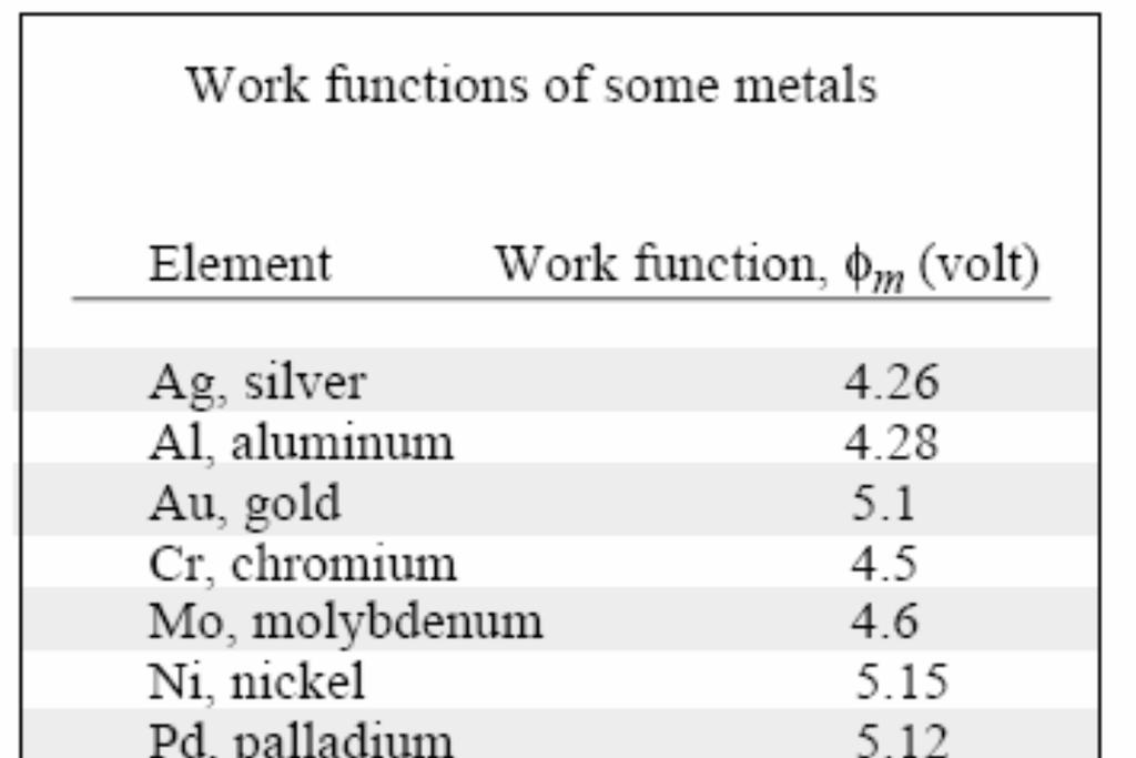
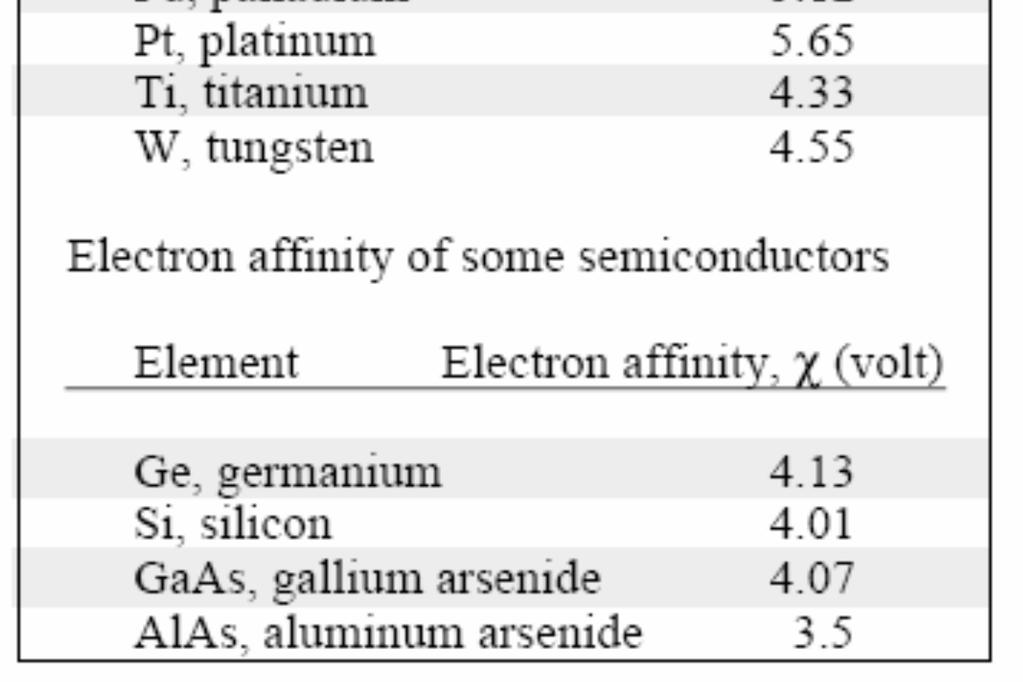
3 Technische Universität Graz Institute of Solid State Physics metal - semiconductor contacts Photoelectric effect Workfunction Electron affinity Interface states Schottky barriers Schottky diodes Ohmic contacts Thermionic emission Tunnel contacts
4 Photoelectric effect hf 0 = e at threshold current workfunction f threshold frequency f 0
5 Singh There is a dipole field at the surface of a metal. This electric field must be overcome for an electron to escape.
6 work function - electron affinity If s < m, the semiconductor bands bend down. If s > m, the semiconductor bands bend up.
7 Singh
8

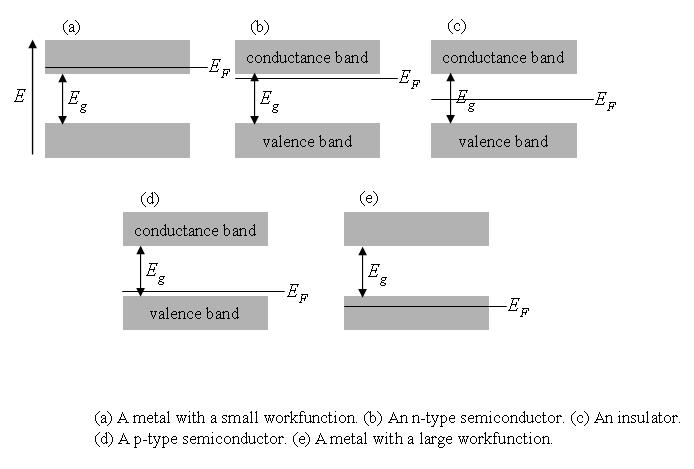
9 p-type Walter Schottky Schottky contact / ohmic contact E F,m metal E F,s Schottky contact E F,m metal E F,s Ohmic contact: linear resistance specific contact resistance: R c J V 1 -cm 2
10 n-type Schottky contact / ohmic contact E F,s Schottky contact E F,m metal E F,m metal E F,s Ohmic contact: linear resistance specific contact resistance: R c J V 1 -cm 2

11 Interface states
12
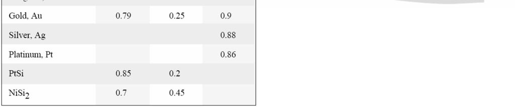
13 Schottky barrier en D E xxn r 0 W x n 2 Vbi en V D V en D x 2 2 xx n
14 CV measurements x p 2 Vbi en V A e NA C x 2 V V p bi C bi V V e N A -2 F m GaAs has larger E g and V bi 1/C 2 ev V Nv ln ( T k T ) N A bi b B


15 Thermionic emission 1901 Richardson Owen Willans Richardson Current from a heated wire is: J A 2 RT exp e kt B Some electrons have a thermal energy that exceeds the work function and escape from the wire.

16 diode Vacuum diodes
 exp exp exp exp kt B kt")

17 Thermionic emission Fermi function ev bi V E F EF E E F E E f( E) exp exp exp exp kt B kt B kt B kt B The density of electrons with enough energy to go over the barriers E exp kt B
18 Thermionic emission n th ev exp kt B I sm ev nth exp kt B I ( 0) ms Ism V ev kt B I Ism Ims Ims e 1
19 Schottky barrier I I sm > I sm ~ 0 ms I ms constant
20 Thermionic emission ev B I I e kt sm Ims I s 1 Nonideality factor = 1
21 Thermionic emission I s * e 2 b AART exp kt B A = Area A R* = Richardson constant n-si A * R = 110 A K -2 cm -2 p-si A * R = 32 A K -2 cm -2 n-gaas A * R = 8 A K -2 cm -2 p-gaas A * R = 74 A K -2 cm -2 Thermionic emission dominates over diffusion current in a Schottky diode.
22 Schottky diodes Majority carrier current dominates. nonideality factor = 1. Fast response, no recombination of electron-hole pairs required. Used as rf mixers. Low turn on voltage - high reverse bias current ev B I I e kt s 1
23 Tunnel contacts For high doping, the Schottky barrier is so thin that electrons can tunnel through it. metal p+ p Degenerate doping at a tunnel contact metal n+ n Tunnel contacts have a linear resistance.
24 Contacts
25 Transport mechanisms Drift Diffusion Thermionic emission Tunneling All mechanisms are always present. One or two transport mechanisms can dominate depending on the device and the bias conditions. In a forward biased pn-junction, diffusion dominates. In a tunnel contact, tunneling dominates. In a Schottky diode, thermionic emission dominates.
26 Technische Universität Graz Institute of Solid State Physics JFETs - MESFETs - MODFETs Junction Field Effect Transistors (JFET) Metal-Semiconductor Field Effect Transistors (MESFET) Modulation Doped Field Effect Transistors (MODFET) n
27 JFET n-channel JFET n For N A >> N D 2 ( ) x n Vbi V en D Depletion mode h x n 2Vbi en D conducting at V g = 0 Enhancement mode h x n 2V bi en D nonconducting at V g = 0
")
28 depletion zone n-channel (power) JFET

29 Power SiC JFET p n p
30 n-channel JFET drain p+ n+ depletion region p n p gate n+ source JFETs are often discrete devices
31 MESFET Metal-Semiconductor Field Effect Transistors n Depletion layer created by Schottky barrier x n 2 ( Vbi V) en D Fast transistors can be realized in n-channel GaAs, however GaAs has a low hole mobility making p-channel devices slower.
32 JFET n D n-channel JFET D G S n-channel JFET x n 2 ( Vbi V) en D G S p-channel JFET 2 Pinch-off at h = x en n Dh Vp 2 V p = pinch-off voltage At Pinch-off, V p = V bi -V.
33 The drain is the side of the transistor that gets pinched off. JFET
8. Schottky contacts / JFETs
 Technische Universität Graz Institute of Solid State Physics 8. Schottky contacts / JFETs Nov. 21, 2018 Technische Universität Graz Institute of Solid State Physics metal - semiconductor contacts Photoelectric
Avalanche breakdown. Impact ionization causes an avalanche of current. Occurs at low doping
 Avalanche breakdown Impact ionization causes an avalanche of current Occurs at low doping Zener tunneling Electrons tunnel from valence band to conduction band Occurs at high doping Tunneling wave decays
Current mechanisms Exam January 27, 2012
 Current mechanisms Exam January 27, 2012 There are four mechanisms that typically cause currents to flow: thermionic emission, diffusion, drift, and tunneling. Explain briefly which kind of current mechanisms
Schottky Rectifiers Zheng Yang (ERF 3017,
 ECE442 Power Semiconductor Devices and Integrated Circuits Schottky Rectifiers Zheng Yang (ERF 3017, email: yangzhen@uic.edu) Power Schottky Rectifier Structure 2 Metal-Semiconductor Contact The work function
Spring Semester 2012 Final Exam
 Spring Semester 2012 Final Exam Note: Show your work, underline results, and always show units. Official exam time: 2.0 hours; an extension of at least 1.0 hour will be granted to anyone. Materials parameters
Chapter 7. The pn Junction
 Chapter 7 The pn Junction Chapter 7 PN Junction PN junction can be fabricated by implanting or diffusing donors into a P-type substrate such that a layer of semiconductor is converted into N type. Converting
PHYSICAL ELECTRONICS(ECE3540) CHAPTER 9 METAL SEMICONDUCTOR AND SEMICONDUCTOR HETERO-JUNCTIONS
 CHAPTER 9 METAL SEMICONDUCTOR AND SEMICONDUCTOR HETERO-JUNCTIONS") PHYSICAL ELECTRONICS(ECE3540) CHAPTER 9 METAL SEMICONDUCTOR AND SEMICONDUCTOR HETERO-JUNCTIONS Tennessee Technological University Monday, November 11, 013 1 Introduction Chapter 4: we considered the semiconductor
PHYSICAL ELECTRONICS(ECE3540) CHAPTER 9 METAL SEMICONDUCTOR AND SEMICONDUCTOR HETERO-JUNCTIONS Tennessee Technological University Monday, November 11, 013 1 Introduction Chapter 4: we considered the semiconductor
PHYSICAL ELECTRONICS(ECE3540) CHAPTER 9 METAL SEMICONDUCTOR AND SEMICONDUCTOR HETERO-JUNCTIONS
 CHAPTER 9 METAL SEMICONDUCTOR AND SEMICONDUCTOR HETERO-JUNCTIONS") PHYSICAL ELECTRONICS(ECE3540) CHAPTER 9 METAL SEMICONDUCTOR AND SEMICONDUCTOR HETERO-JUNCTIONS Tennessee Technological University Wednesday, October 30, 013 1 Introduction Chapter 4: we considered the
PHYSICAL ELECTRONICS(ECE3540) CHAPTER 9 METAL SEMICONDUCTOR AND SEMICONDUCTOR HETERO-JUNCTIONS Tennessee Technological University Wednesday, October 30, 013 1 Introduction Chapter 4: we considered the
Semiconductor Device Physics
 1 emiconductor Device Physics Lecture 8 http://zitompul.wordpress.com 2 0 1 3 emiconductor Device Physics 2 M Contacts and chottky Diodes 3 M Contact The metal-semiconductor (M) contact plays a very important
Institute of Solid State Physics. Technische Universität Graz. Exam. Feb 2, 10:00-11:00 P2
 Technische Universität Graz nstitute of Solid State Physics Exam Feb 2, 10:00-11:00 P2 Exam Four questions, two from the online list. Calculator is ok. No notes. Explain some concept: (tunnel contact,
Consider a uniformly doped PN junction, in which one region of the semiconductor is uniformly doped with acceptor atoms and the adjacent region is
 CHAPTER 7 The PN Junction Consider a uniformly doped PN junction, in which one region of the semiconductor is uniformly doped with acceptor atoms and the adjacent region is uniformly doped with donor atoms.
Semiconductor Physics and Devices
 The pn Junction 1) Charge carriers crossing the junction. 3) Barrier potential Semiconductor Physics and Devices Chapter 8. The pn Junction Diode 2) Formation of positive and negative ions. 4) Formation
Metal Semiconductor Contacts
 Metal Semiconductor Contacts The investigation of rectification in metal-semiconductor contacts was first described by Braun [33-35], who discovered in 1874 the asymmetric nature of electrical conduction
EECS130 Integrated Circuit Devices
 EECS130 Integrated Circuit Devices Professor Ali Javey 10/02/2007 MS Junctions, Lecture 2 MOS Cap, Lecture 1 Reading: finish chapter14, start chapter16 Announcements Professor Javey will hold his OH at
Semiconductor Devices
 Semiconductor Devices - 2014 Lecture Course Part of SS Module PY4P03 Dr. P. Stamenov School of Physics and CRANN, Trinity College, Dublin 2, Ireland Hilary Term, TCD 17 th of Jan 14 Metal-Semiconductor
Memories Bipolar Transistors
 Technische Universität Graz nstitute of Solid State Physics Memories Bipolar Transistors Technische Universität Graz nstitute of Solid State Physics Exams February 5 March 7 April 18 June 27 Exam Four
Figure 3.1 (p. 141) Figure 3.2 (p. 142)
 Figure 3.2 (p. 142)") Figure 3.1 (p. 141) Allowed electronic-energy-state systems for two isolated materials. States marked with an X are filled; those unmarked are empty. System 1 is a qualitative representation of a metal;
Figure 3.1 (p. 141) Allowed electronic-energy-state systems for two isolated materials. States marked with an X are filled; those unmarked are empty. System 1 is a qualitative representation of a metal;
ECE 340 Lecture 35 : Metal- Semiconductor Junctions Class Outline:
 ECE 340 Lecture 35 : - Junctions Class Outline: Ideal - Contacts Rectifying Contacts Ohmic Contacts Things you should know when you leave Key Questions What happens to the bands when we make contact between
JFET/MESFET. JFET: small gate current (reverse leakage of the gate-to-channel junction) More gate leakage than MOSFET, less than bipolar.
 More gate leakage than MOSFET, less than bipolar.") JFET/MESFET JFET: small gate current (reverse leakage of the gate-to-channel junction) More gate leakage than MOSFET, less than bipolar. JFET has higher transconductance than the MOSFET. Used in low-noise,
JFET/MESFET JFET: small gate current (reverse leakage of the gate-to-channel junction) More gate leakage than MOSFET, less than bipolar. JFET has higher transconductance than the MOSFET. Used in low-noise,
Session 6: Solid State Physics. Diode
 Session 6: Solid State Physics Diode 1 Outline A B C D E F G H I J 2 Definitions / Assumptions Homojunction: the junction is between two regions of the same material Heterojunction: the junction is between
JFETs - MESFETs - MODFETs
 Technische Universität raz Institute of Solid State Physics JFETs - MESFETs - MOFETs JFET n n-channel JFET S n-channel JFET x n 2 ( Vbi V) en S p-channel JFET 2 Pinch-off at h = x en n h Vp 2 V p = pinch-off
1 Name: Student number: DEPARTMENT OF PHYSICS AND PHYSICAL OCEANOGRAPHY MEMORIAL UNIVERSITY OF NEWFOUNDLAND. Fall :00-11:00
 1 Name: DEPARTMENT OF PHYSICS AND PHYSICAL OCEANOGRAPHY MEMORIAL UNIVERSITY OF NEWFOUNDLAND Final Exam Physics 3000 December 11, 2012 Fall 2012 9:00-11:00 INSTRUCTIONS: 1. Answer all seven (7) questions.
Physics of Semiconductors 8 th
 Physics of Semiconductors 8 th 2016.6.6 Shingo Katsumoto Department of Physics, Institute for Solid State Physics University of Tokyo Review of pn junction Estimation of builtin potential Depletion layer
n N D n p = n i p N A
 Summary of electron and hole concentration in semiconductors Intrinsic semiconductor: E G n kt i = pi = N e 2 0 Donor-doped semiconductor: n N D where N D is the concentration of donor impurity Acceptor-doped
UNIVERSITY OF CALIFORNIA College of Engineering Department of Electrical Engineering and Computer Sciences. EECS 130 Professor Ali Javey Fall 2006
 UNIVERSITY OF CALIFORNIA College of Engineering Department of Electrical Engineering and Computer Sciences EECS 130 Professor Ali Javey Fall 2006 Midterm 2 Name: SID: Closed book. Two sheets of notes are
Review Energy Bands Carrier Density & Mobility Carrier Transport Generation and Recombination
 Review Energy Bands Carrier Density & Mobility Carrier Transport Generation and Recombination The Metal-Semiconductor Junction: Review Energy band diagram of the metal and the semiconductor before (a)
Semiconductor Physics. Lecture 6
 Semiconductor Physics Lecture 6 Recap pn junction and the depletion region Driven by the need to have no gradient in the fermi level free carriers migrate across the pn junction leaving a region with few
3. Two-dimensional systems
 3. Two-dimensional systems Image from IBM-Almaden 1 Introduction Type I: natural layered structures, e.g., graphite (with C nanostructures) Type II: artificial structures, heterojunctions Great technological
GaN based transistors
 GaN based transistors S FP FP dielectric G SiO 2 Al x Ga 1-x N barrier i-gan Buffer i-sic D Transistors "The Transistor was probably the most important invention of the 20th Century The American Institute
MOS Capacitors ECE 2204
 MOS apacitors EE 2204 Some lasses of Field Effect Transistors Metal-Oxide-Semiconductor Field Effect Transistor MOSFET, which will be the type that we will study in this course. Metal-Semiconductor Field
Final Examination EE 130 December 16, 1997 Time allotted: 180 minutes
 Final Examination EE 130 December 16, 1997 Time allotted: 180 minutes Problem 1: Semiconductor Fundamentals [30 points] A uniformly doped silicon sample of length 100µm and cross-sectional area 100µm 2
Semiconductor Physics fall 2012 problems
 Semiconductor Physics fall 2012 problems 1. An n-type sample of silicon has a uniform density N D = 10 16 atoms cm -3 of arsenic, and a p-type silicon sample has N A = 10 15 atoms cm -3 of boron. For each
Introductory Nanotechnology ~ Basic Condensed Matter Physics ~
 Introductory Nanotechnology ~ Basic Condensed Matter Physics ~ Atsufumi Hirohata Department of Electronics Quick Review over the Last Lecture Classic model : Dulong-Petit empirical law c V, mol 3R 0 E
Introduction to Power Semiconductor Devices
 ECE442 Power Semiconductor Devices and Integrated Circuits Introduction to Power Semiconductor Devices Zheng Yang (ERF 3017, email: yangzhen@uic.edu) Power Semiconductor Devices Applications System Ratings
12. Memories / Bipolar transistors
 Technische Universität Graz Institute of Solid State Physics 12. Memories / Bipolar transistors Jan. 9, 2019 Technische Universität Graz Institute of Solid State Physics Exams January 31 March 8 May 17
Semiconductor Physical Electronics
 Semiconductor Physical Electronics Sheng S. Li Department of Electrical Engineering University of Florida Gainesville, Florida Plenum Press New York and London Contents CHAPTER 1. Classification of Solids
Peak Electric Field. Junction breakdown occurs when the peak electric field in the PN junction reaches a critical value. For the N + P junction,
 Peak Electric Field Junction breakdown occurs when the peak electric field in the P junction reaches a critical value. For the + P junction, qa E ( x) ( xp x), s W dep 2 s ( bi Vr ) 2 s potential barrier
Lecture 04 Review of MOSFET
 ECE 541/ME 541 Microelectronic Fabrication Techniques Lecture 04 Review of MOSFET Zheng Yang (ERF 3017, email: yangzhen@uic.edu) What is a Transistor? A Switch! An MOS Transistor V GS V T V GS S Ron D
Lecture 9: Metal-semiconductor junctions
 Lecture 9: Metal-semiconductor junctions Contents 1 Introduction 1 2 Metal-metal junction 1 2.1 Thermocouples.......................... 2 3 Schottky junctions 4 3.1 Forward bias............................
Session 0: Review of Solid State Devices. From Atom to Transistor
 Session 0: Review of Solid State Devices From Atom to Transistor 1 Objective To Understand: how Diodes, and Transistors operate! p n p+ n p- n+ n+ p 2 21 Century Alchemy! Ohm s law resistivity Resistivity
- A free electron in CB "meets" a hole in VB: the excess energy -> a photon energy.
 5.4. Recombination and Minority Carrier Injection 5.4.1 Direct and Indirect Recombination A free electron in CB "meets" a hole in VB: the excess energy > a photon energy. Energy CB ψ cb (k cb ) ψ vb (k
Section 12: Intro to Devices
 Section 12: Intro to Devices Extensive reading materials on reserve, including Robert F. Pierret, Semiconductor Device Fundamentals Bond Model of Electrons and Holes Si Si Si Si Si Si Si Si Si Silicon
Semiconductor Physics Problems 2015
 Semiconductor Physics Problems 2015 Page and figure numbers refer to Semiconductor Devices Physics and Technology, 3rd edition, by SM Sze and M-K Lee 1. The purest semiconductor crystals it is possible
Problem 9.20 Threshold bias for an n-channel MOSFET: In the text we used a criterion that the inversion of the MOSFET channel occurs when V s = ;2 F w
 Prof. Jasprit Singh Fall 2001 EECS 320 Homework 11 The nals for this course are set for Friday December 14, 6:30 8:30 pm and Friday Dec. 21, 10:30 am 12:30 pm. Please choose one of these times and inform
Theory of Electrical Characterization of Semiconductors
 Theory of Electrical Characterization of Semiconductors P. Stallinga Universidade do Algarve U.C.E.H. A.D.E.E.C. OptoElectronics SELOA Summer School May 2000, Bologna (It) Overview Devices: bulk Schottky
EE 3329 Electronic Devices Syllabus ( Extended Play )
") EE 3329 - Electronic Devices Syllabus EE 3329 Electronic Devices Syllabus ( Extended Play ) The University of Texas at El Paso The following concepts can be part of the syllabus for the Electronic Devices
EE 3329 - Electronic Devices Syllabus EE 3329 Electronic Devices Syllabus ( Extended Play ) The University of Texas at El Paso The following concepts can be part of the syllabus for the Electronic Devices
Semiconductor Junctions
 8 Semiconductor Junctions Almost all solar cells contain junctions between different materials of different doping. Since these junctions are crucial to the operation of the solar cell, we will discuss
Appendix 1: List of symbols
 Appendix 1: List of symbols Symbol Description MKS Units a Acceleration m/s 2 a 0 Bohr radius m A Area m 2 A* Richardson constant m/s A C Collector area m 2 A E Emitter area m 2 b Bimolecular recombination
MTLE-6120: Advanced Electronic Properties of Materials. Semiconductor p-n junction diodes. Reading: Kasap ,
 MTLE-6120: Advanced Electronic Properties of Materials 1 Semiconductor p-n junction diodes Reading: Kasap 6.1-6.5, 6.9-6.12 Metal-semiconductor contact potential 2 p-type n-type p-type n-type Same semiconductor
Lecture 12: MOS Capacitors, transistors. Context
 Lecture 12: MOS Capacitors, transistors Context In the last lecture, we discussed PN diodes, and the depletion layer into semiconductor surfaces. Small signal models In this lecture, we will apply those
* motif: a single or repeated design or color
 Chapter 2. Structure A. Electronic structure vs. Geometric structure B. Clean surface vs. Adsorbate covered surface (substrate + overlayer) C. Adsorbate structure - how are the adsorbed molecules bound
MENA9510 characterization course: Capacitance-voltage (CV) measurements
 measurements") MENA9510 characterization course: Capacitance-voltage (CV) measurements 30.10.2017 Halvard Haug Outline Overview of interesting sample structures Ohmic and schottky contacts Why C-V for solar cells? The
MENA9510 characterization course: Capacitance-voltage (CV) measurements 30.10.2017 Halvard Haug Outline Overview of interesting sample structures Ohmic and schottky contacts Why C-V for solar cells? The
Sample Exam # 2 ECEN 3320 Fall 2013 Semiconductor Devices October 28, 2013 Due November 4, 2013
 Sample Exam # 2 ECEN 3320 Fall 203 Semiconductor Devices October 28, 203 Due November 4, 203. Below is the capacitance-voltage curve measured from a Schottky contact made on GaAs at T 300 K. Figure : Capacitance
Part 1: MetalMetal Contacts Workfunction Differences Flat band (a) (Pt) = 5.36 ev Pt Vacuum Fermi level Electrons Mo Vacuum Fermi level Electrons (Mo)
 (Pt) = 5.36 ev Pt Vacuum Fermi level Electrons Mo Vacuum Fermi level Electrons (Mo)") Applications Using Band Diagrams and Fermi Energy Level Applications to Devices Physics Physics Homojunctions Heterojunctions pn junction metals/c junctions diodes pnp junction pnp Bipolar transistors
Applications Using Band Diagrams and Fermi Energy Level Applications to Devices Physics Physics Homojunctions Heterojunctions pn junction metals/c junctions diodes pnp junction pnp Bipolar transistors
Effective masses in semiconductors
 Effective masses in semiconductors The effective mass is defined as: In a solid, the electron (hole) effective mass represents how electrons move in an applied field. The effective mass reflects the inverse
Fundamentals of Semiconductor Physics
 Fall 2007 Fundamentals of Semiconductor Physics 万 歆 Zhejiang Institute of Modern Physics xinwan@zimp.zju.edu.cn http://zimp.zju.edu.cn/~xinwan/ Transistor technology evokes new physics The objective of
junctions produce nonlinear current voltage characteristics which can be exploited
 Chapter 6 P-N DODES Junctions between n-and p-type semiconductors are extremely important foravariety of devices. Diodes based on p-n junctions produce nonlinear current voltage characteristics which can
Transistors - a primer
 ransistors - a primer What is a transistor? Solid-state triode - three-terminal device, with voltage (or current) at third terminal used to control current between other two terminals. wo types: bipolar
9. Semiconductor Devices /Phonons
 Technische Universität Graz Institute of Solid State Physics 9. Semiconductor Devices /Phonons Oct 29, 2018 p and n profiles p n V bi ~ 1 V E c W ~ 1 m E F E max ~ 10 4 V/cm ev bi E v p Ev E F Nv exp kt
Classification of Solids
 Classification of Solids Classification by conductivity, which is related to the band structure: (Filled bands are shown dark; D(E) = Density of states) Class Electron Density Density of States D(E) Examples
Sheng S. Li. Semiconductor Physical Electronics. Second Edition. With 230 Figures. 4) Springer
 Springer") Sheng S. Li Semiconductor Physical Electronics Second Edition With 230 Figures 4) Springer Contents Preface 1. Classification of Solids and Crystal Structure 1 1.1 Introduction 1 1.2 The Bravais Lattice
Sheng S. Li Semiconductor Physical Electronics Second Edition With 230 Figures 4) Springer Contents Preface 1. Classification of Solids and Crystal Structure 1 1.1 Introduction 1 1.2 The Bravais Lattice
Thermionic emission vs. drift-diffusion vs. p-n junction
 6.772/SMA5111 - Compound Semiconductors Lecture 4 - Carrier flow in heterojunctions - Outline A look at current models for m-s junctions (old business) Thermionic emission vs. drift-diffusion vs. p-n junction
Semiconductor Physics fall 2012 problems
 Semiconductor Physics fall 2012 problems 1. An n-type sample of silicon has a uniform density N D = 10 16 atoms cm -3 of arsenic, and a p-type silicon sample has N A = 10 15 atoms cm -3 of boron. For each
Lecture 2. Introduction to semiconductors Structures and characteristics in semiconductors. Fabrication of semiconductor sensor
 Lecture 2 Introduction to semiconductors Structures and characteristics in semiconductors Semiconductor p-n junction Metal Oxide Silicon structure Semiconductor contact Fabrication of semiconductor sensor
Lecture 2. Introduction to semiconductors Structures and characteristics in semiconductors
 Lecture 2 Introduction to semiconductors Structures and characteristics in semiconductors Semiconductor p-n junction Metal Oxide Silicon structure Semiconductor contact Literature Glen F. Knoll, Radiation
For the following statements, mark ( ) for true statement and (X) for wrong statement and correct it.
 for true statement and (X) for wrong statement and correct it.") Benha University Faculty of Engineering Shoubra Electrical Engineering Department First Year communications. Answer all the following questions Illustrate your answers with sketches when necessary. The
Benha University Faculty of Engineering Shoubra Electrical Engineering Department First Year communications. Answer all the following questions Illustrate your answers with sketches when necessary. The
Surfaces, Interfaces, and Layered Devices
 Surfaces, Interfaces, and Layered Devices Building blocks for nanodevices! W. Pauli: God made solids, but surfaces were the work of Devil. Surfaces and Interfaces 1 Interface between a crystal and vacuum
The pn junction. [Fonstad, Ghione]
![The pn junction. [Fonstad, Ghione]](/thumbs/93/112370833.jpg "The pn junction. [Fonstad, Ghione]") The pn junction [Fonstad, Ghione] Band diagram On the vertical axis: potential energy of the electrons On the horizontal axis: now there is nothing: later we ll put the position qf s : work function (F
The pn junction [Fonstad, Ghione] Band diagram On the vertical axis: potential energy of the electrons On the horizontal axis: now there is nothing: later we ll put the position qf s : work function (F
MOS Capacitor MOSFET Devices. MOSFET s. INEL Solid State Electronics. Manuel Toledo Quiñones. ECE Dept. UPRM.
 INEL 6055 - Solid State Electronics ECE Dept. UPRM 20th March 2006 Definitions MOS Capacitor Isolated Metal, SiO 2, Si Threshold Voltage qφ m metal d vacuum level SiO qχ 2 E g /2 qφ F E C E i E F E v qφ
EE 130 Intro to MS Junctions Week 6 Notes. What is the work function? Energy to excite electron from Fermi level to the vacuum level
 EE 13 Intro to S Junctions eek 6 Notes Problem 1 hat is the work function? Energy to ecite electron from Fermi level to the vacuum level Electron affinity of 4.5eV Electron affinity of Ge 4.eV orkfunction
R. Ludwig and G. Bogdanov RF Circuit Design: Theory and Applications 2 nd edition. Figures for Chapter 6
 R. Ludwig and G. Bogdanov RF Circuit Design: Theory and Applications 2 nd edition Figures for Chapter 6 Free electron Conduction band Hole W g W C Forbidden Band or Bandgap W V Electron energy Hole Valence
Module-6: Schottky barrier capacitance-impurity concentration
 6.1 Introduction: Module-6: Schottky barrier capacitance-impurity concentration The electric current flowing across a metal semiconductor interface is generally non-linear with respect to the applied bias
MSE 310/ECE 340: Electrical Properties of Materials Fall 2014 Department of Materials Science and Engineering Boise State University
 MSE 310/ECE 340: Electrical Properties of Materials Fall 2014 Department of Materials Science and Engineering Boise State University Practice Final Exam 1 Read the questions carefully Label all figures
ECE-305: Spring 2018 Exam 2 Review
 ECE-305: Spring 018 Exam Review Pierret, Semiconductor Device Fundamentals (SDF) Chapter 3 (pp. 75-138) Chapter 5 (pp. 195-6) Professor Peter Bermel Electrical and Computer Engineering Purdue University,
Operation and Modeling of. The MOS Transistor. Second Edition. Yannis Tsividis Columbia University. New York Oxford OXFORD UNIVERSITY PRESS
 Operation and Modeling of The MOS Transistor Second Edition Yannis Tsividis Columbia University New York Oxford OXFORD UNIVERSITY PRESS CONTENTS Chapter 1 l.l 1.2 1.3 1.4 1.5 1.6 1.7 Chapter 2 2.1 2.2
Thermionic Emission Theory
 hapter 4. PN and Metal-Semiconductor Junction Thermionic Emiion Theory Energy band diagram of a Schottky contact with a forward bia V applied between the metal and the emiconductor. Electron concentration
Concepts & Equations. Applications: Devices
 Concepts & Equations Applications: Devices Concepts & Equations Applications: Devices Current = (charge) x (velocity) Ch1-4 Ch5-6 Concepts & Equations Applications: Devices Concepts & Equations Ch1 Landscape
ρ ρ LED access resistances d A W d s n s p p p W the output window size p-layer d p series access resistance d n n-layer series access resistance
 LED access resistances W the output window size p-layer series access resistance d p n-layer series access resistance d n The n-layer series access resistance R = ρ s n where the resistivity of the n-layer
V BI. H. Föll: kiel.de/matwis/amat/semi_en/kap_2/backbone/r2_2_4.html. different electrochemical potentials (i.e.
 Consider the the band diagram for a homojunction, formed when two bits of the same type of semicondutor (e.g. Si) are doped p and ntype and then brought into contact. Electrons in the two bits have different
CHAPTER 4: P-N P N JUNCTION Part 2. M.N.A. Halif & S.N. Sabki
 CHAPTER 4: P-N P N JUNCTION Part 2 Part 2 Charge Storage & Transient Behavior Junction Breakdown Heterojunction CHARGE STORAGE & TRANSIENT BEHAVIOR Once injected across the junction, the minority carriers
ECE 340 Lecture 39 : MOS Capacitor II
 ECE 340 Lecture 39 : MOS Capacitor II Class Outline: Effects of Real Surfaces Threshold Voltage MOS Capacitance-Voltage Analysis Things you should know when you leave Key Questions What are the effects
Typical example of the FET: MEtal Semiconductor FET (MESFET)
") Typical example of the FET: MEtal Semiconductor FET (MESFET) Conducting channel (RED) is made of highly doped material. The electron concentration in the channel n = the donor impurity concentration N
Typical example of the FET: MEtal Semiconductor FET (MESFET) Conducting channel (RED) is made of highly doped material. The electron concentration in the channel n = the donor impurity concentration N
Section 12: Intro to Devices
 Section 12: Intro to Devices Extensive reading materials on reserve, including Robert F. Pierret, Semiconductor Device Fundamentals EE143 Ali Javey Bond Model of Electrons and Holes Si Si Si Si Si Si Si
Lecture 17 - p-n Junction. October 11, Ideal p-n junction in equilibrium 2. Ideal p-n junction out of equilibrium
 6.72J/3.43J - Integrated Microelectronic Devices - Fall 22 Lecture 17-1 Lecture 17 - p-n Junction October 11, 22 Contents: 1. Ideal p-n junction in equilibrium 2. Ideal p-n junction out of equilibrium
EECS130 Integrated Circuit Devices
 EECS130 Integrated Circuit Devices Professor Ali Javey 9/18/2007 P Junctions Lecture 1 Reading: Chapter 5 Announcements For THIS WEEK OLY, Prof. Javey's office hours will be held on Tuesday, Sept 18 3:30-4:30
Solid State Electronics. Final Examination
 The University of Toledo EECS:4400/5400/7400 Solid State Electronic Section elssf08fs.fm - 1 Solid State Electronics Final Examination Problems Points 1. 1. 14 3. 14 Total 40 Was the exam fair? yes no
MOSFET: Introduction
 E&CE 437 Integrated VLSI Systems MOS Transistor 1 of 30 MOSFET: Introduction Metal oxide semiconductor field effect transistor (MOSFET) or MOS is widely used for implementing digital designs Its major
Long Channel MOS Transistors
 Long Channel MOS Transistors The theory developed for MOS capacitor (HO #2) can be directly extended to Metal-Oxide-Semiconductor Field-Effect transistors (MOSFET) by considering the following structure:
Electrical Characteristics of MOS Devices
 Electrical Characteristics of MOS Devices The MOS Capacitor Voltage components Accumulation, Depletion, Inversion Modes Effect of channel bias and substrate bias Effect of gate oide charges Threshold-voltage
Semiconductor Module
 Semiconductor Module Optics Seminar July 18, 2018 Yosuke Mizuyama, Ph.D. COMSOL, Inc. The COMSOL Product Suite Governing Equations Semiconductor Schrödinger Equation Semiconductor Optoelectronics, FD Semiconductor
Schottky Diodes (M-S Contacts)
") Schottky Diodes (M-S Contacts) Three MITs of the Day Band diagrams for ohmic and rectifying Schottky contacts Similarity to and difference from bipolar junctions on electrostatic and IV characteristics.
Schottky Diodes (M-S Contacts) Three MITs of the Day Band diagrams for ohmic and rectifying Schottky contacts Similarity to and difference from bipolar junctions on electrostatic and IV characteristics.
ECE-305: Fall 2017 Metal Oxide Semiconductor Devices
 C-305: Fall 2017 Metal Oxide Semiconductor Devices Pierret, Semiconductor Device Fundamentals (SDF) Chapters 15+16 (pp. 525-530, 563-599) Professor Peter Bermel lectrical and Computer ngineering Purdue
Semiconductor Integrated Process Design (MS 635)
") Semiconductor Integrated Process Design (MS 635) Instructor: Prof. Keon Jae Lee - Office: 응용공학동 #4306, Tel: #3343 - Email: keonlee@kaist.ac.kr Lecture: (Tu, Th), 1:00-2:15 #2425 Office hour: Tues & Thur
Semiconductor Integrated Process Design (MS 635) Instructor: Prof. Keon Jae Lee - Office: 응용공학동 #4306, Tel: #3343 - Email: keonlee@kaist.ac.kr Lecture: (Tu, Th), 1:00-2:15 #2425 Office hour: Tues & Thur
Electrical Characteristics of Multilayer MoS 2 FET s
 Electrical Characteristics of Multilayer MoS 2 FET s with MoS 2 /Graphene Hetero-Junction Contacts Joon Young Kwak,* Jeonghyun Hwang, Brian Calderon, Hussain Alsalman, Nini Munoz, Brian Schutter, and Michael
Lecture 6: 2D FET Electrostatics
 Lecture 6: 2D FET Electrostatics 2016-02-01 Lecture 6, High Speed Devices 2014 1 Lecture 6: III-V FET DC I - MESFETs Reading Guide: Liu: 323-337 (he mainly focuses on the single heterostructure FET) Jena:
Electronic Circuits 1. Transistor Devices. Contents BJT and FET Characteristics Operations. Prof. C.K. Tse: Transistor devices
 Electronic Circuits 1 Transistor Devices Contents BJT and FET Characteristics Operations 1 What is a transistor? Three-terminal device whose voltage-current relationship is controlled by a third voltage
PN Junction
 P Junction 2017-05-04 Definition Power Electronics = semiconductor switches are used Analogue amplifier = high power loss 250 200 u x 150 100 u Udc i 50 0 0 50 100 150 200 250 300 350 400 i,u dc i,u u
III.6. METAL SEMICONDUCTOR CONTACT BIAS
 .6. MEAL SEMCONUCOR CONAC BAS 1. Work purpose he determination of the potential difference that appears at the contact surface between a metal and a semiconductor, potential difference that is known under
MOS CAPACITOR AND MOSFET
 EE336 Semiconductor Devices 1 MOS CAPACITOR AND MOSFET Dr. Mohammed M. Farag Ideal MOS Capacitor Semiconductor Devices Physics and Technology Chapter 5 EE336 Semiconductor Devices 2 MOS Capacitor Structure
! PN Junction. ! MOS Transistor Topology. ! Threshold. ! Operating Regions. " Resistive. " Saturation. " Subthreshold (next class)
") ESE370: ircuitlevel Modeling, Design, and Optimization for Digital Systems Lec 7: September 20, 2017 MOS Transistor Operating Regions Part 1 Today! PN Junction! MOS Transistor Topology! Threshold! Operating
ESE370: ircuitlevel Modeling, Design, and Optimization for Digital Systems Lec 7: September 20, 2017 MOS Transistor Operating Regions Part 1 Today! PN Junction! MOS Transistor Topology! Threshold! Operating