JFET/MESFET. JFET: small gate current (reverse leakage of the gate-to-channel junction) More gate leakage than MOSFET, less than bipolar.
|
|
|
- Nathaniel Cross
- 6 years ago
- Views:
Transcription
1 JFET/MESFET JFET: small gate current (reverse leakage of the gate-to-channel junction) More gate leakage than MOSFET, less than bipolar. JFET has higher transconductance than the MOSFET. Used in low-noise, high input-impedance op-amps and sometimes used in switching applications. MESFET: usually constructed in compound semiconductor technologies lacking high quality surface passivation such as GaAs, InP, or SiC, and are faster but more expensive than silicon-based JFETs or MOSFETs. Production MESFETs are operated up to approximately 30 GHz, and are commonly used for microwave frequency communications and radar. Majority carrier device (like Schottky diode).

2 SiC JFET p n p
3 MODFET (HEMT) Modulation doped field effect transistor (MODFET) High electron mobility transistor (HEMT) Modulation doped field effect transistor High electron mobility transistor V T = Threshold voltage = voltage where charge is depleted
4 Heterostructure pn junction formed from two semiconductors with different band gaps
5 PhD Thesis Sergey Smirnov MODFET/HEMT undoped channel HEMT: HEMT devices are found in cell phones, electronic warfare systems, microwave and millimeter wave communications, radar, and radio astronomy.
6 MODFET (HEMT) j = nev = neµ E d n y I = jzt = Zeµ n E n s y t is the thickness of the 2DEG n s is the sheet charge at the interface in C/cm 2. n = n s t VG V( y) is the voltage between the gate and the 2DEG n s = 0 when V V( y) = V G T gate y 2DEG q = CV ( ) en ( y) = C V V ( y) V s g G T
7 MODFET (HEMT) ( ) en ( y) = C V V ( y) V s g G B T is the charge on the 2DEG at point y The charge is zero when V V ( y) = V G B T solve for n s n s ( y) = ( ( ) ) C V V y V g G B T e Substitute this in Ohm's law: I = jzt = Zeµ n E n s y
8 MODFET (HEMT) n s I = jzt = Zeµ n E ( y) = n s y ( ( ) ) C V V y V g G T substitute n s in the top equation and substitute e E y = dv ( y) dy ( ( )) I= Zµ CV V V y n G T dv ( y) dy integrate along the length of the channel L V D 0 0 ( ( )) Idy = Zµ C V V V y dv n G T 2 Z VD ( ) L µ ID = nc VG VT VD 2
9 MODFET (HEMT) 2 Z VD n ( G T) D L µ 2 I = C V V V di Z nc VG VT VD dv = L µ = D ( ) 0 Set the derivative = 0 to find saturation voltage ( ) V = V V sat G T Substitute the saturation voltage into the formula at the top to find saturation current I = Z CV V 2L µ ( ) 2 sat n G T
10
11 MODFET/HEMT HEMT: HEMT devices are found in many types of equipment ranging from cell phones and DBS receivers to electronic warfare systems, microwave and millimeter wave communications, radar, and radio astronomy. 600 GHz

12 GaN-HEMT Source: Oliver Hilt, Bauteile aus GaN, ETG Tagung Bad Nauheim 2011

13 Quantized conduction R K = h/e 2 = (18) Ω Quantized conductance of point contacts in a two-dimensional electron gas, B. J. van Wees, H. van Houten, C. W. J. Beenakker, J. G. Williamson, L. P. Kouwenhoven, D. van der Marel, and C. T. Foxon, Phys. Rev. Lett. 60, (1988).
 Ω Formation and Manipulation of a Metallic")

14 Quantized conduction R K = h/e 2 = (18) Ω Formation and Manipulation of a Metallic Wire of Single Gold Atoms, A. I. Yanson, G. Rubio Bollinger, H.E. van den Brom, N. Agraït, J.M. van Ruitenbeek, Nature Oct
15 Quantum Hall Effect Bz ρxy = = ne v = 1, 2, 3 h ve 2 Shubnikov-De Haas oscillations Resistance standard (18) Ω

16 Technische Universität Graz Institute of Solid State Physics MOSFETs functions as a switch ~ 1 billion /chip n - channel p - channel
17 Self-aligned fabrication p-si 100 wafer
18 Dry oxidation SiO 2 gate oxide p-si
19 gate oxide HfO 2 SiO 2 p-si
 30 70 μω cm Conductive diffusion barrier SiO 2 /HfO")
20 photoresist polysilicon CVD: SiH 580 to 650 C TiN (CVD) μω cm Conductive diffusion barrier SiO 2 /HfO 2 p-si
21 Implant polysilicon gate Expose resist Develop Etch poly and TiN Strip resist Implant source and drain TiN p-si SiO 2 /HfO 2
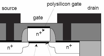
22 Self-aligned fabrication polysilicon gate n+ n+ p-si
23 Spacer PECVD SiN x SiN x polysilicon gate n+ n+ p-si
24 Spacer Etch back to leave only sidewalls SiN x polysilicon gate n+ n+ p-si
25 Implant polysilicon gate n+ n+ p-si
26 Salicide (Self-aligned silicide) Transition metal (Ti, Co,W) is deposited (CVD). During a high temperature step is reacts to a silicide (TiSi 2 ). No silicide is formed on nitride or oxide. polysilicon gate TiSi 2 (metal) n+ n+ p-si

27 CMOS Fransila
28 MOS capacitor
29 Accumulation no depletion layer metal oxide semiconductor -t ox 0 ev N A n i2 /N A
30 Accumulation E
31 Depletion
32 Flat band voltage no depletion layer ev fb N A x n i2 /N A If φ s = φ m, the flatband voltage is the zero bias voltage
33 Zero bias metal oxide semiconductor -t ox 0 eφ m Al 4.1 ev p+ poly 4.05 ev n+ poly 5.05 ev Can be in accumulation or depletion depending on workfunctions

34 Weak Inversion Majority carriers at x = 0 change from p to n n > p at the interface

35 Threshold voltage n = N A Strong inversion: n = N A at x = 0, the semiconductor-oxide interface
36 Inversion n > N A at x = 0, the semiconductor-oxide interface
37 MOS capacitor In inversion, the charge in the inversion layer is: mobile charge Q = -C ox (V G -V B -V T ) fixed charge Mobile charge per unit area Specific capacitance F/m 2
38 MOS capacitor n

39 Poisson equation 2 V = ρ ε
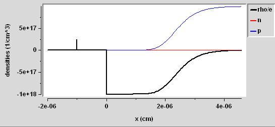
40 charge density (depletion) x p e t < x< 0 ρ( x) = 0 ox 0 < x < x ρ( x) = en p x < x ρ( x) = 0 p A
41 electric field (depletion) E E is decreased by a factor of the dielectric constant ε = r E E vacuum dielectric ε ox = 4 ε s = 12
42 electric field x p -e x< t Ex ( ) = 0 ox ε S + tox < x< 0 Ex ( ) = Ex ( = 0 ) = ε en A 0 < x< xp Ex ( ) = x x ε x < x Ex ( ) = 0 p ox s ( p) en x ε A ox p x p
43 electrostatic potential x< t φ( x) = φ ox x p x p IB 2 en Axp en Axp tox < x< 0 φ( x) = φp + + x 2ε ε en A 0 < x< x φ( x) = φ + x x 2ε x < x φ( x) = φ p gate s ( ) p p p s (We still don't know x p ) p ox 2 ( )
44 Band bending at inversion Far on the p side n = N A at threshold n 2 n i EF E c = = Nc exp NA kt B 2 n i EF Ec = kt B ln NANc At the interface, n = N A EF E c = Ncexp kt B N N A A EF Ec = kt B ln Nc The voltage between the semiconductor-oxide interface and the body ev kt N kt n V kt N V 2 2 A i A IB = B ln B ln + FB = B ln 2 + FB Nc NANc ni V IB is the voltage between the interface and the body ev IB ln ( a) ln ( b) ln a = b
45 Strong inversion n s = N A at the semiconductor-oxide interface ev kt N V kt N V 2 A A IB = B ln 2 ln 2 + FB = B + FB ni ni The depletion width remains constant in inversion. ln 2 ( a ) = 2ln ( a)
46 Depletion width in strong inversion V IB = en x A 2ε 2 p ev IB N A = 2kBT ln ni x 2 V N = ε = 2 ε ktln IB A p(max) 2 B en A e N A ni The depletion width remains constant in inversion.
47 Depletion width
48 Electric field at semi-oxide interface at strong inversion ev IB N A (strong inversion) = 2kBT ln ni E s VIB 2VIB N A N A = 2 = = 2 kt B ln xp(max) 2εV ε n IB i en A V IB = E s x p /2 = area of the triangle ε 2ε N 2 A N ln A Eox = Es = kt B εox εox ε ni p

49 Threshold voltage ( strong inversion) ( strong inversion) V = E t + V + V T ox ox IB FB V T N A NkT A B ln 2εt n ox i kt B N A = + 2 ln + V εox ε e ni FB εt ε ox ox E inversion V IB Small V T requires a small t ox and a large ε ox.
50 MOS capacitance C ox = ε t ox ox C j = ε x p C 1 1 = + Cox C j 1 Accumulation Inversion V FB

51 CCD devices
JFETs - MESFETs - MODFETs
 Technische Universität raz Institute of Solid State Physics JFETs - MESFETs - MOFETs JFET n n-channel JFET S n-channel JFET x n 2 ( Vbi V) en S p-channel JFET 2 Pinch-off at h = x en n h Vp 2 V p = pinch-off
Schottky diodes. JFETs - MESFETs - MODFETs
 Technische Universität Graz Institute of Solid State Physics Schottky diodes JFETs - MESFETs - MODFETs Quasi Fermi level When the charge carriers are not in equilibrium the Fermi energy can be different
8. Schottky contacts / JFETs
 Technische Universität Graz Institute of Solid State Physics 8. Schottky contacts / JFETs Nov. 21, 2018 Technische Universität Graz Institute of Solid State Physics metal - semiconductor contacts Photoelectric
Avalanche breakdown. Impact ionization causes an avalanche of current. Occurs at low doping
 Avalanche breakdown Impact ionization causes an avalanche of current Occurs at low doping Zener tunneling Electrons tunnel from valence band to conduction band Occurs at high doping Tunneling wave decays
Fundamentals of the Metal Oxide Semiconductor Field-Effect Transistor
 Triode Working FET Fundamentals of the Metal Oxide Semiconductor Field-Effect Transistor The characteristics of energy bands as a function of applied voltage. Surface inversion. The expression for the
Lecture 12: MOS Capacitors, transistors. Context
 Lecture 12: MOS Capacitors, transistors Context In the last lecture, we discussed PN diodes, and the depletion layer into semiconductor surfaces. Small signal models In this lecture, we will apply those
MOS Capacitors ECE 2204
 MOS apacitors EE 2204 Some lasses of Field Effect Transistors Metal-Oxide-Semiconductor Field Effect Transistor MOSFET, which will be the type that we will study in this course. Metal-Semiconductor Field
GaN based transistors
 GaN based transistors S FP FP dielectric G SiO 2 Al x Ga 1-x N barrier i-gan Buffer i-sic D Transistors "The Transistor was probably the most important invention of the 20th Century The American Institute
ECE-305: Fall 2017 MOS Capacitors and Transistors
 ECE-305: Fall 2017 MOS Capacitors and Transistors Pierret, Semiconductor Device Fundamentals (SDF) Chapters 15+16 (pp. 525-530, 563-599) Professor Peter Bermel Electrical and Computer Engineering Purdue
MOSFET: Introduction
 E&CE 437 Integrated VLSI Systems MOS Transistor 1 of 30 MOSFET: Introduction Metal oxide semiconductor field effect transistor (MOSFET) or MOS is widely used for implementing digital designs Its major
Technische Universität Graz. Institute of Solid State Physics. 11. MOSFETs
 Technische Universität Graz Institute of Solid State Physics 11. MOSFETs Dec. 12, 2018 Gradual channel approximation accumulation depletion inversion http://lampx.tugraz.at/~hadley/psd/l10/gradualchannelapprox.php
Section 12: Intro to Devices
 Section 12: Intro to Devices Extensive reading materials on reserve, including Robert F. Pierret, Semiconductor Device Fundamentals EE143 Ali Javey Bond Model of Electrons and Holes Si Si Si Si Si Si Si
SECTION: Circle one: Alam Lundstrom. ECE 305 Exam 5 SOLUTIONS: Spring 2016 April 18, 2016 M. A. Alam and M.S. Lundstrom Purdue University
 NAME: PUID: SECTION: Circle one: Alam Lundstrom ECE 305 Exam 5 SOLUTIONS: April 18, 2016 M A Alam and MS Lundstrom Purdue University This is a closed book exam You may use a calculator and the formula
Field effect = Induction of an electronic charge due to an electric field Example: Planar capacitor
 JFETs AND MESFETs Introduction Field effect = Induction of an electronic charge due to an electric field Example: Planar capacitor Why would an FET made of a planar capacitor with two metal plates, as
Lecture 11: MOS Transistor
 Lecture 11: MOS Transistor Prof. Niknejad Lecture Outline Review: MOS Capacitors Regions MOS Capacitors (3.8 3.9) CV Curve Threshold Voltage MOS Transistors (4.1 4.3): Overview Cross-section and layout
Electrical Characteristics of MOS Devices
 Electrical Characteristics of MOS Devices The MOS Capacitor Voltage components Accumulation, Depletion, Inversion Modes Effect of channel bias and substrate bias Effect of gate oide charges Threshold-voltage
MOS CAPACITOR AND MOSFET
 EE336 Semiconductor Devices 1 MOS CAPACITOR AND MOSFET Dr. Mohammed M. Farag Ideal MOS Capacitor Semiconductor Devices Physics and Technology Chapter 5 EE336 Semiconductor Devices 2 MOS Capacitor Structure
Content. MIS Capacitor. Accumulation Depletion Inversion MOS CAPACITOR. A Cantoni Digital Switching
 Content MIS Capacitor Accumulation Depletion Inversion MOS CAPACITOR 1 MIS Capacitor Metal Oxide C ox p-si C s Components of a capacitance model for the MIS structure 2 MIS Capacitor- Accumulation ρ( x)
Section 12: Intro to Devices
 Section 12: Intro to Devices Extensive reading materials on reserve, including Robert F. Pierret, Semiconductor Device Fundamentals Bond Model of Electrons and Holes Si Si Si Si Si Si Si Si Si Silicon
Lecture 04 Review of MOSFET
 ECE 541/ME 541 Microelectronic Fabrication Techniques Lecture 04 Review of MOSFET Zheng Yang (ERF 3017, email: yangzhen@uic.edu) What is a Transistor? A Switch! An MOS Transistor V GS V T V GS S Ron D
Final Examination EE 130 December 16, 1997 Time allotted: 180 minutes
 Final Examination EE 130 December 16, 1997 Time allotted: 180 minutes Problem 1: Semiconductor Fundamentals [30 points] A uniformly doped silicon sample of length 100µm and cross-sectional area 100µm 2
MOS Transistors. Prof. Krishna Saraswat. Department of Electrical Engineering Stanford University Stanford, CA
 MOS Transistors Prof. Krishna Saraswat Department of Electrical Engineering S Stanford, CA 94305 saraswat@stanford.edu 1 1930: Patent on the Field-Effect Transistor! Julius Lilienfeld filed a patent describing
Lecture 6: 2D FET Electrostatics
 Lecture 6: 2D FET Electrostatics 2016-02-01 Lecture 6, High Speed Devices 2014 1 Lecture 6: III-V FET DC I - MESFETs Reading Guide: Liu: 323-337 (he mainly focuses on the single heterostructure FET) Jena:
ECE 340 Lecture 39 : MOS Capacitor II
 ECE 340 Lecture 39 : MOS Capacitor II Class Outline: Effects of Real Surfaces Threshold Voltage MOS Capacitance-Voltage Analysis Things you should know when you leave Key Questions What are the effects
Lecture 15 OUTLINE. MOSFET structure & operation (qualitative) Review of electrostatics The (N)MOS capacitor
 Review of electrostatics The (N)MOS capacitor") Lecture 15 OUTLINE MOSFET structure & operation (qualitative) Review of electrostatics The (N)MOS capacitor Electrostatics t ti Charge vs. voltage characteristic Reading: Chapter 6.1 6.2.1 EE105 Fall 2007
Lecture 15 OUTLINE MOSFET structure & operation (qualitative) Review of electrostatics The (N)MOS capacitor Electrostatics t ti Charge vs. voltage characteristic Reading: Chapter 6.1 6.2.1 EE105 Fall 2007
Institute of Solid State Physics. Technische Universität Graz. Exam. Feb 2, 10:00-11:00 P2
 Technische Universität Graz nstitute of Solid State Physics Exam Feb 2, 10:00-11:00 P2 Exam Four questions, two from the online list. Calculator is ok. No notes. Explain some concept: (tunnel contact,
Scaling Issues in Planar FET: Dual Gate FET and FinFETs
 Scaling Issues in Planar FET: Dual Gate FET and FinFETs Lecture 12 Dr. Amr Bayoumi Fall 2014 Advanced Devices (EC760) Arab Academy for Science and Technology - Cairo 1 Outline Scaling Issues for Planar
Chapter 3 Basics Semiconductor Devices and Processing
 Chapter 3 Basics Semiconductor Devices and Processing Hong Xiao, Ph. D. www2.austin.cc.tx.us/hongxiao/book.htm Hong Xiao, Ph. D. www2.austin.cc.tx.us/hongxiao/book.htm 1 Objectives Identify at least two
Lecture 3: CMOS Transistor Theory
 Lecture 3: CMOS Transistor Theory Outline Introduction MOS Capacitor nmos I-V Characteristics pmos I-V Characteristics Gate and Diffusion Capacitance 2 Introduction So far, we have treated transistors
Part 4: Heterojunctions - MOS Devices. MOSFET Current Voltage Characteristics
 MOS Device Uses: Part 4: Heterojunctions - MOS Devices MOSCAP capacitor: storing charge, charge-coupled device (CCD), etc. MOSFET transistor: switch, current amplifier, dynamic random access memory (DRAM-volatile),
1. The MOS Transistor. Electrical Conduction in Solids
 Electrical Conduction in Solids!The band diagram describes the energy levels for electron in solids.!the lower filled band is named Valence Band.!The upper vacant band is named conduction band.!the distance
The Intrinsic Silicon
 The Intrinsic ilicon Thermally generated electrons and holes Carrier concentration p i =n i ni=1.45x10 10 cm-3 @ room temp Generally: n i = 3.1X10 16 T 3/2 e -1.21/2KT cm -3 T= temperature in K o (egrees
The Devices: MOS Transistors
 The Devices: MOS Transistors References: Semiconductor Device Fundamentals, R. F. Pierret, Addison-Wesley Digital Integrated Circuits: A Design Perspective, J. Rabaey et.al. Prentice Hall NMOS Transistor
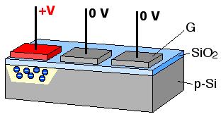
Typical example of the FET: MEtal Semiconductor FET (MESFET)
") Typical example of the FET: MEtal Semiconductor FET (MESFET) Conducting channel (RED) is made of highly doped material. The electron concentration in the channel n = the donor impurity concentration N
Typical example of the FET: MEtal Semiconductor FET (MESFET) Conducting channel (RED) is made of highly doped material. The electron concentration in the channel n = the donor impurity concentration N
1 Name: Student number: DEPARTMENT OF PHYSICS AND PHYSICAL OCEANOGRAPHY MEMORIAL UNIVERSITY OF NEWFOUNDLAND. Fall :00-11:00
 1 Name: DEPARTMENT OF PHYSICS AND PHYSICAL OCEANOGRAPHY MEMORIAL UNIVERSITY OF NEWFOUNDLAND Final Exam Physics 3000 December 11, 2012 Fall 2012 9:00-11:00 INSTRUCTIONS: 1. Answer all seven (7) questions.
12. Memories / Bipolar transistors
 Technische Universität Graz Institute of Solid State Physics 12. Memories / Bipolar transistors Jan. 9, 2019 Technische Universität Graz Institute of Solid State Physics Exams January 31 March 8 May 17
Extensive reading materials on reserve, including
 Section 12: Intro to Devices Extensive reading materials on reserve, including Robert F. Pierret, Semiconductor Device Fundamentals EE143 Ali Javey Bond Model of Electrons and Holes Si Si Si Si Si Si Si
MENA9510 characterization course: Capacitance-voltage (CV) measurements
 measurements") MENA9510 characterization course: Capacitance-voltage (CV) measurements 30.10.2017 Halvard Haug Outline Overview of interesting sample structures Ohmic and schottky contacts Why C-V for solar cells? The
MENA9510 characterization course: Capacitance-voltage (CV) measurements 30.10.2017 Halvard Haug Outline Overview of interesting sample structures Ohmic and schottky contacts Why C-V for solar cells? The
Semiconductor Devices. C. Hu: Modern Semiconductor Devices for Integrated Circuits Chapter 5
 Semiconductor Devices C. Hu: Modern Semiconductor Devices for Integrated Circuits Chapter 5 Global leader in environmental and industrial measurement Wednesday 3.2. afternoon Tour around facilities & lecture
Appendix 1: List of symbols
 Appendix 1: List of symbols Symbol Description MKS Units a Acceleration m/s 2 a 0 Bohr radius m A Area m 2 A* Richardson constant m/s A C Collector area m 2 A E Emitter area m 2 b Bimolecular recombination
ESE 570: Digital Integrated Circuits and VLSI Fundamentals
 ESE 570: Digital Integrated Circuits and VLSI Fundamentals Lec 4: January 23, 2018 MOS Transistor Theory, MOS Model Penn ESE 570 Spring 2018 Khanna Lecture Outline! CMOS Process Enhancements! Semiconductor
Lecture 2. Introduction to semiconductors Structures and characteristics in semiconductors
 Lecture 2 Introduction to semiconductors Structures and characteristics in semiconductors Semiconductor p-n junction Metal Oxide Silicon structure Semiconductor contact Literature Glen F. Knoll, Radiation
MSE 310/ECE 340: Electrical Properties of Materials Fall 2014 Department of Materials Science and Engineering Boise State University
 MSE 310/ECE 340: Electrical Properties of Materials Fall 2014 Department of Materials Science and Engineering Boise State University Practice Final Exam 1 Read the questions carefully Label all figures
ECE 497 JS Lecture - 12 Device Technologies
 ECE 497 JS Lecture - 12 Device Technologies Spring 2004 Jose E. Schutt-Aine Electrical & Computer Engineering University of Illinois jose@emlab.uiuc.edu 1 NMOS Transistor 2 ρ Source channel charge density
an introduction to Semiconductor Devices
 an introduction to Semiconductor Devices Donald A. Neamen Chapter 6 Fundamentals of the Metal-Oxide-Semiconductor Field-Effect Transistor Introduction: Chapter 6 1. MOSFET Structure 2. MOS Capacitor -
The Devices. Digital Integrated Circuits A Design Perspective. Jan M. Rabaey Anantha Chandrakasan Borivoje Nikolic. July 30, 2002
 Digital Integrated Circuits A Design Perspective Jan M. Rabaey Anantha Chandrakasan Borivoje Nikolic The Devices July 30, 2002 Goal of this chapter Present intuitive understanding of device operation Introduction
Metal-oxide-semiconductor field effect transistors (2 lectures)
") Metal-ide-semiconductor field effect transistors ( lectures) MOS physics (brief in book) Current-voltage characteristics - pinch-off / channel length modulation - weak inversion - velocity saturation -
Metal-ide-semiconductor field effect transistors ( lectures) MOS physics (brief in book) Current-voltage characteristics - pinch-off / channel length modulation - weak inversion - velocity saturation -
MOS Capacitor MOSFET Devices. MOSFET s. INEL Solid State Electronics. Manuel Toledo Quiñones. ECE Dept. UPRM.
 INEL 6055 - Solid State Electronics ECE Dept. UPRM 20th March 2006 Definitions MOS Capacitor Isolated Metal, SiO 2, Si Threshold Voltage qφ m metal d vacuum level SiO qχ 2 E g /2 qφ F E C E i E F E v qφ
EE 560 MOS TRANSISTOR THEORY
 1 EE 560 MOS TRANSISTOR THEORY PART 1 TWO TERMINAL MOS STRUCTURE V G (GATE VOLTAGE) 2 GATE OXIDE SiO 2 SUBSTRATE p-type doped Si (N A = 10 15 to 10 16 cm -3 ) t ox V B (SUBSTRATE VOLTAGE) EQUILIBRIUM:
Lecture 15 OUTLINE. MOSFET structure & operation (qualitative) Review of electrostatics The (N)MOS capacitor
 Review of electrostatics The (N)MOS capacitor") Lecture 15 OUTLINE MOSFET structure & operation (qualitative) Review of electrostatics The (N)MOS capacitor Electrostatics Charge vs. voltage characteristic Reading: Chapter 6.1 6.2.1 EE15 Spring 28 Lecture
Lecture 15 OUTLINE MOSFET structure & operation (qualitative) Review of electrostatics The (N)MOS capacitor Electrostatics Charge vs. voltage characteristic Reading: Chapter 6.1 6.2.1 EE15 Spring 28 Lecture
MOS Transistor I-V Characteristics and Parasitics
 ECEN454 Digital Integrated Circuit Design MOS Transistor I-V Characteristics and Parasitics ECEN 454 Facts about Transistors So far, we have treated transistors as ideal switches An ON transistor passes
Introduction and Background
 Analog CMOS Integrated Circuit Design Introduction and Background Dr. Jawdat Abu-Taha Department of Electrical and Computer Engineering Islamic University of Gaza jtaha@iugaza.edu.ps 1 Marking Assignments
FIELD-EFFECT TRANSISTORS
 FIEL-EFFECT TRANSISTORS 1 Semiconductor review 2 The MOS capacitor 2 The enhancement-type N-MOS transistor 3 I-V characteristics of enhancement MOSFETS 4 The output characteristic of the MOSFET in saturation
EE105 - Fall 2006 Microelectronic Devices and Circuits
 EE105 - Fall 2006 Microelectronic Devices and Circuits Prof. Jan M. Rabaey (jan@eecs) Lecture 7: MOS Transistor Some Administrative Issues Lab 2 this week Hw 2 due on We Hw 3 will be posted same day MIDTERM
Metallic: 2n 1. +n 2. =3q Armchair structure always metallic = 2
 Properties of CNT d = 2.46 n 2 2 1 + n1n2 + n2 2π Metallic: 2n 1 +n 2 =3q Armchair structure always metallic a) Graphite Valence(π) and Conduction(π*) states touch at six points(fermi points) Carbon Nanotube:
UNIVERSITY OF CALIFORNIA College of Engineering Department of Electrical Engineering and Computer Sciences. EECS 130 Professor Ali Javey Fall 2006
 UNIVERSITY OF CALIFORNIA College of Engineering Department of Electrical Engineering and Computer Sciences EECS 130 Professor Ali Javey Fall 2006 Midterm 2 Name: SID: Closed book. Two sheets of notes are
MOS Transistor Properties Review
 MOS Transistor Properties Review 1 VLSI Chip Manufacturing Process Photolithography: transfer of mask patterns to the chip Diffusion or ion implantation: selective doping of Si substrate Oxidation: SiO
ELEN0037 Microelectronic IC Design. Prof. Dr. Michael Kraft
 ELEN0037 Microelectronic IC Design Prof. Dr. Michael Kraft Lecture 2: Technological Aspects Technology Passive components Active components CMOS Process Basic Layout Scaling CMOS Technology Integrated
Choice of V t and Gate Doping Type
 Choice of V t and Gate Doping Type To make circuit design easier, it is routine to set V t at a small positive value, e.g., 0.4 V, so that, at V g = 0, the transistor does not have an inversion layer and
Transistors - a primer
 ransistors - a primer What is a transistor? Solid-state triode - three-terminal device, with voltage (or current) at third terminal used to control current between other two terminals. wo types: bipolar
Lecture 5: CMOS Transistor Theory
 Lecture 5: CMOS Transistor Theory Slides courtesy of Deming Chen Slides based on the initial set from David Harris CMOS VLSI Design Outline q q q q q q q Introduction MOS Capacitor nmos I-V Characteristics
6.012 Electronic Devices and Circuits
 Page 1 of 12 YOUR NAME Department of Electrical Engineering and Computer Science Massachusetts Institute of Technology 6.012 Electronic Devices and Circuits FINAL EXAMINATION Open book. Notes: 1. Unless
Lecture 2. Introduction to semiconductors Structures and characteristics in semiconductors. Fabrication of semiconductor sensor
 Lecture 2 Introduction to semiconductors Structures and characteristics in semiconductors Semiconductor p-n junction Metal Oxide Silicon structure Semiconductor contact Fabrication of semiconductor sensor
R. Ludwig and G. Bogdanov RF Circuit Design: Theory and Applications 2 nd edition. Figures for Chapter 6
 R. Ludwig and G. Bogdanov RF Circuit Design: Theory and Applications 2 nd edition Figures for Chapter 6 Free electron Conduction band Hole W g W C Forbidden Band or Bandgap W V Electron energy Hole Valence
ESE 570 MOS TRANSISTOR THEORY Part 1. Kenneth R. Laker, University of Pennsylvania, updated 5Feb15
 ESE 570 MOS TRANSISTOR THEORY Part 1 TwoTerminal MOS Structure 2 GATE Si Oxide interface n n Mass Action Law VB 2 Chemical Periodic Table Donors American Chemical Society (ACS) Acceptors Metalloids 3 Ideal
EE 434 Lecture 12. Process Flow (wrap up) Device Modeling in Semiconductor Processes
 Device Modeling in Semiconductor Processes") EE 434 Lecture 12 Process Flow (wrap up) Device Modeling in Semiconductor Processes Quiz 6 How have process engineers configured a process to assure that the thickness of the gate oxide for the p-channel
EE 434 Lecture 12 Process Flow (wrap up) Device Modeling in Semiconductor Processes Quiz 6 How have process engineers configured a process to assure that the thickness of the gate oxide for the p-channel
MOS Transistor Theory
 CHAPTER 3 MOS Transistor Theory Outline 2 1. Introduction 2. Ideal I-V Characteristics 3. Nonideal I-V Effects 4. C-V Characteristics 5. DC Transfer Characteristics 6. Switch-level RC Delay Models MOS
Lecture 2. Introduction to semiconductors Structures and characteristics in semiconductors
 Lecture 2 Introduction to semiconductors Structures and characteristics in semiconductors Semiconductor p-n junction Metal Oxide Silicon structure Semiconductor contact Literature Glen F. Knoll, Radiation
ECE-305: Fall 2017 Metal Oxide Semiconductor Devices
 C-305: Fall 2017 Metal Oxide Semiconductor Devices Pierret, Semiconductor Device Fundamentals (SDF) Chapters 15+16 (pp. 525-530, 563-599) Professor Peter Bermel lectrical and Computer ngineering Purdue
Integrated Circuits & Systems
 Federal University of Santa Catarina Center for Technology Computer Science & Electronics Engineering Integrated Circuits & Systems INE 5442 Lecture 10 MOSFET part 1 guntzel@inf.ufsc.br ual-well Trench-Isolated
ESE 570: Digital Integrated Circuits and VLSI Fundamentals
 ESE 570: Digital Integrated Circuits and VLSI Fundamentals Lec 4: January 29, 2019 MOS Transistor Theory, MOS Model Penn ESE 570 Spring 2019 Khanna Lecture Outline! CMOS Process Enhancements! Semiconductor
EE115C Winter 2017 Digital Electronic Circuits. Lecture 3: MOS RC Model, CMOS Manufacturing
 EE115C Winter 2017 Digital Electronic Circuits Lecture 3: MOS RC Model, CMOS Manufacturing Agenda MOS Transistor: RC Model (pp. 104-113) S R on D CMOS Manufacturing Process (pp. 36-46) S S C GS G G C GD
CMOS Devices. PN junctions and diodes NMOS and PMOS transistors Resistors Capacitors Inductors Bipolar transistors
 CMOS Devices PN junctions and diodes NMOS and PMOS transistors Resistors Capacitors Inductors Bipolar transistors PN Junctions Diffusion causes depletion region D.R. is insulator and establishes barrier
Digital Integrated Circuits A Design Perspective. Jan M. Rabaey Anantha Chandrakasan Borivoje Nikolic. The Devices. July 30, Devices.
 Digital Integrated Circuits A Design Perspective Jan M. Rabaey Anantha Chandrakasan Borivoje Nikolic The July 30, 2002 1 Goal of this chapter Present intuitive understanding of device operation Introduction
! CMOS Process Enhancements. ! Semiconductor Physics. " Band gaps. " Field Effects. ! MOS Physics. " Cut-off. " Depletion.
 ESE 570: Digital Integrated Circuits and VLSI Fundamentals Lec 4: January 3, 018 MOS Transistor Theory, MOS Model Lecture Outline! CMOS Process Enhancements! Semiconductor Physics " Band gaps " Field Effects!
ECE 305 Exam 5 SOLUTIONS: Spring 2015 April 17, 2015 Mark Lundstrom Purdue University
 NAME: PUID: : ECE 305 Exam 5 SOLUTIONS: April 17, 2015 Mark Lundstrom Purdue University This is a closed book exam. You may use a calculator and the formula sheet at the end of this exam. Following the
ECE 342 Electronic Circuits. 3. MOS Transistors
 ECE 342 Electronic Circuits 3. MOS Transistors Jose E. Schutt-Aine Electrical & Computer Engineering University of Illinois jschutt@emlab.uiuc.edu 1 NMOS Transistor Typically L = 0.1 to 3 m, W = 0.2 to
EE105 - Fall 2005 Microelectronic Devices and Circuits
 EE105 - Fall 005 Microelectronic Devices and Circuits ecture 7 MOS Transistor Announcements Homework 3, due today Homework 4 due next week ab this week Reading: Chapter 4 1 ecture Material ast lecture
Lecture 12: MOSFET Devices
 Lecture 12: MOSFET Devices Gu-Yeon Wei Division of Engineering and Applied Sciences Harvard University guyeon@eecs.harvard.edu Wei 1 Overview Reading S&S: Chapter 5.1~5.4 Supplemental Reading Background
The Devices. Devices
 The The MOS Transistor Gate Oxyde Gate Source n+ Polysilicon Drain n+ Field-Oxyde (SiO 2 ) p-substrate p+ stopper Bulk Contact CROSS-SECTION of NMOS Transistor Cross-Section of CMOS Technology MOS transistors
Device Models (PN Diode, MOSFET )
") Device Models (PN Diode, MOSFET ) Instructor: Steven P. Levitan steve@ece.pitt.edu TA: Gayatri Mehta, José Martínez Book: Digital Integrated Circuits: A Design Perspective; Jan Rabaey Lab Notes: Handed
Device Models (PN Diode, MOSFET ) Instructor: Steven P. Levitan steve@ece.pitt.edu TA: Gayatri Mehta, José Martínez Book: Digital Integrated Circuits: A Design Perspective; Jan Rabaey Lab Notes: Handed
Classification of Solids
 Classification of Solids Classification by conductivity, which is related to the band structure: (Filled bands are shown dark; D(E) = Density of states) Class Electron Density Density of States D(E) Examples
Lecture 150 Basic IC Processes (10/10/01) Page ECE Analog Integrated Circuits and Systems P.E. Allen
 Page ECE Analog Integrated Circuits and Systems P.E. Allen") Lecture 150 Basic IC Processes (10/10/01) Page 1501 LECTURE 150 BASIC IC PROCESSES (READING: TextSec. 2.2) INTRODUCTION Objective The objective of this presentation is: 1.) Introduce the fabrication of
Lecture 150 Basic IC Processes (10/10/01) Page 1501 LECTURE 150 BASIC IC PROCESSES (READING: TextSec. 2.2) INTRODUCTION Objective The objective of this presentation is: 1.) Introduce the fabrication of
Lecture 6 PN Junction and MOS Electrostatics(III) Metal-Oxide-Semiconductor Structure
 Metal-Oxide-Semiconductor Structure") Lecture 6 PN Junction and MOS Electrostatics(III) Metal-Oxide-Semiconductor Structure Outline 1. Introduction to MOS structure 2. Electrostatics of MOS in thermal equilibrium 3. Electrostatics of MOS with
Lecture 6 PN Junction and MOS Electrostatics(III) Metal-Oxide-Semiconductor Structure Outline 1. Introduction to MOS structure 2. Electrostatics of MOS in thermal equilibrium 3. Electrostatics of MOS with
Effects of Antimony Near SiO 2 /SiC Interfaces
 Effects of Antimony Near SiO 2 /SiC Interfaces P.M. Mooney, A.F. Basile, and Zenan Jiang Simon Fraser University, Burnaby, BC, V5A1S6, Canada and Yongju Zheng, Tamara Isaacs-Smith Smith, Aaron Modic, and
The Devices. Digital Integrated Circuits A Design Perspective. Jan M. Rabaey Anantha Chandrakasan Borivoje Nikolic. July 30, 2002
 igital Integrated Circuits A esign Perspective Jan M. Rabaey Anantha Chandrakasan Borivoje Nikolic The evices July 30, 2002 Goal of this chapter Present intuitive understanding of device operation Introduction
Student Number: CARLETON UNIVERSITY SELECTED FINAL EXAMINATION QUESTIONS
 Name: CARLETON UNIVERSITY SELECTE FINAL EXAMINATION QUESTIONS URATION: 6 HOURS epartment Name & Course Number: ELEC 3908 Course Instructors: S. P. McGarry Authorized Memoranda: Non-programmable calculators
Current mechanisms Exam January 27, 2012
 Current mechanisms Exam January 27, 2012 There are four mechanisms that typically cause currents to flow: thermionic emission, diffusion, drift, and tunneling. Explain briefly which kind of current mechanisms
MOS Transistor Theory
 MOS Transistor Theory So far, we have viewed a MOS transistor as an ideal switch (digital operation) Reality: less than ideal EE 261 Krish Chakrabarty 1 Introduction So far, we have treated transistors
Device Models (PN Diode, MOSFET )
") Device Models (PN Diode, MOSFET ) Instructor: Steven P. Levitan steve@ece.pitt.edu TA: Gayatri Mehta, José Martínez Book: Digital Integrated Circuits: A Design Perspective; Jan Rabaey Lab Notes: Handed
Device Models (PN Diode, MOSFET ) Instructor: Steven P. Levitan steve@ece.pitt.edu TA: Gayatri Mehta, José Martínez Book: Digital Integrated Circuits: A Design Perspective; Jan Rabaey Lab Notes: Handed
! CMOS Process Enhancements. ! Semiconductor Physics. " Band gaps. " Field Effects. ! MOS Physics. " Cut-off. " Depletion.
 ESE 570: Digital Integrated Circuits and VLSI Fundamentals Lec 4: January 9, 019 MOS Transistor Theory, MOS Model Lecture Outline CMOS Process Enhancements Semiconductor Physics Band gaps Field Effects
Memories Bipolar Transistors
 Technische Universität Graz nstitute of Solid State Physics Memories Bipolar Transistors Technische Universität Graz nstitute of Solid State Physics Exams February 5 March 7 April 18 June 27 Exam Four
Semiconductor Integrated Process Design (MS 635)
") Semiconductor Integrated Process Design (MS 635) Instructor: Prof. Keon Jae Lee - Office: 응용공학동 #4306, Tel: #3343 - Email: keonlee@kaist.ac.kr Lecture: (Tu, Th), 1:00-2:15 #2425 Office hour: Tues & Thur
Semiconductor Integrated Process Design (MS 635) Instructor: Prof. Keon Jae Lee - Office: 응용공학동 #4306, Tel: #3343 - Email: keonlee@kaist.ac.kr Lecture: (Tu, Th), 1:00-2:15 #2425 Office hour: Tues & Thur
Surfaces, Interfaces, and Layered Devices
 Surfaces, Interfaces, and Layered Devices Building blocks for nanodevices! W. Pauli: God made solids, but surfaces were the work of Devil. Surfaces and Interfaces 1 Interface between a crystal and vacuum
Long Channel MOS Transistors
 Long Channel MOS Transistors The theory developed for MOS capacitor (HO #2) can be directly extended to Metal-Oxide-Semiconductor Field-Effect transistors (MOSFET) by considering the following structure:
ESE370: Circuit-Level Modeling, Design, and Optimization for Digital Systems
 ESE370: Circuit-Level Modeling, Design, and Optimization for Digital Systems Lec 6: September 18, 2017 MOS Model You are Here: Transistor Edition! Previously: simple models (0 and 1 st order) " Comfortable
Semiconductor Physics Problems 2015
 Semiconductor Physics Problems 2015 Page and figure numbers refer to Semiconductor Devices Physics and Technology, 3rd edition, by SM Sze and M-K Lee 1. The purest semiconductor crystals it is possible
Chapter 4 Field-Effect Transistors
 Chapter 4 Field-Effect Transistors Microelectronic Circuit Design Richard C. Jaeger Travis N. Blalock 5/5/11 Chap 4-1 Chapter Goals Describe operation of MOSFETs. Define FET characteristics in operation
EECS130 Integrated Circuit Devices
 EECS130 Integrated Circuit Devices Professor Ali Javey 10/02/2007 MS Junctions, Lecture 2 MOS Cap, Lecture 1 Reading: finish chapter14, start chapter16 Announcements Professor Javey will hold his OH at
Lecture 7 PN Junction and MOS Electrostatics(IV) Metal Oxide Semiconductor Structure (contd.)
 Metal Oxide Semiconductor Structure (contd.)") Lecture 7 PN Junction and MOS Electrostatics(IV) Metal Oxide Semiconductor Structure (contd.) Outline 1. Overview of MOS electrostatics under bias 2. Depletion regime 3. Flatband 4. Accumulation regime
Lecture 7 PN Junction and MOS Electrostatics(IV) Metal Oxide Semiconductor Structure (contd.) Outline 1. Overview of MOS electrostatics under bias 2. Depletion regime 3. Flatband 4. Accumulation regime