GaN HEMT Reliability
|
|
|
- Dulcie Wheeler
- 6 years ago
- Views:
Transcription

1 GaN HEMT Reliability J. A. del Alamo and J. Joh Microsystems Technology Laboratories, MIT ESREF 2009 Arcachon, Oct. 5-9, 2009 Acknowledgements: ARL (DARPA-WBGS program), ONR (DRIFT-MURI program) Jose Jimenez, Sefa Demirtas 1
2 1. Introduction: GaN Reliability GaN HEMT: commercial technology since 2005 Great recent strides in reliability: MTTF=10 7 h at 150 C and 40 V demonstrated [Jimenez, IRPS 2008] Unique issues about GaN HEMT reliability: No native substrate (use SiC, Si, sapphire) mismatch defects High-voltage operation very high electric fields (~10 7 V/cm) Strong piezoelectric materials: high electric field high mechanical stress Electron channel charge set by polarization, not dopants Work to do before demonstrating consistent, reproducible reliability with solid understanding behind: When will we be able to put GaN in space? 2
3 Outline 1. Introduction 2. Experimental 3. Results 4. Hypothesis for high-voltage degradation mechanism: Defect formation through inverse piezoelectric effect 5. Discussion 6. Conclusions 3
4 2. Experimental GaN HEMT Reliability Test Chip 3.25 x mm2 DC and mmw HEMTs HEMTs with different dimensions (Lrd, Lrs, Lg, Wg, #fingers) HEMTs with different orientations (0, 30o, 60o, 90o) TLM s, side-gate FET, FATFET Most devices completed before vias Implemented by BAE, TriQuint and Nitronex with own design rules 4
5 DC Stress Experiments START Characterization I Dmax, R S, R D, I Goff, V T Trapping Analysis Electrical Stress V DS, V GS (or I D ) 5
6 Characterization Suite Comprehensive, three sets of measurements: Coarse characterization: basic device parameters Fine characterization: + complete set of I-V characteristics (output, transfer, gate, subthreshold, kink) Trap analysis: transient analysis under various pulsing conditions Fast: Coarse characterization: <20 secs Fine characterization: <1 min Trap analysis: <10 min Frequent: Coarse characterization: every 1-2 mins Fine characterization, trap analysis: before, after, at key points Benign : 100 executions to produce change <2% change in any extracted parameter 6


7 DC Stress Schemes Stress-recovery experiments: to study trapping behavior Step-stress experiments: to study a variety of conditions in a single device (for improved experimental efficiency) Step-stress-recovery experiments: to study trap formation under different conditions in a single device 7
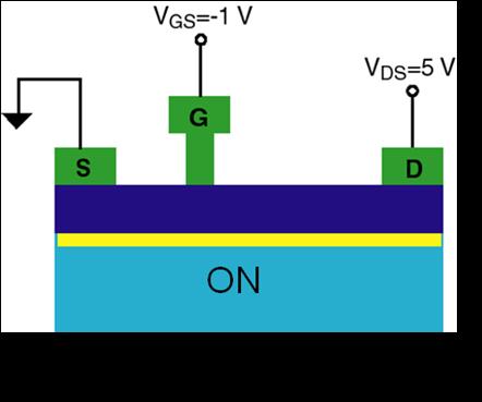

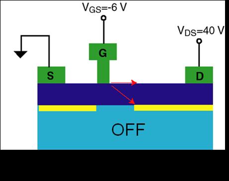
8 Electrical Stress Bias Points Hot electrons! 8
9 Typical GaN HEMT Source Gate Drain GaN Cap AlGaN GaN SiN 2DEG Typical values: t = nm x = 25-30% SiC Substrate Standard device with integrated field plate : L G =0.25 um, W=4x100 um f T =40 GHz, I Dmax =1.2 A/mm P out =8 W/mm, 10 GHz, V D =40 V Test device: W=2x25 um 9


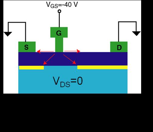
10 3. Results: V DS =0 Degradation V DS =0 step-stress; V DG : 10 to 50 V, 1 V/step, 1 min/step I Dmax I Dmax R ON g m 10


11 V DS =0 Degradation V DS =0 step-stress; V DG : 10 to 50 V, 1 V/step, 1 min/step I Goff I Gon I Doff I Goff I Gon 11


12 V DS =0 Degradation Joh, EDL 2008 Critical voltage for degradation: At V crit 21 V, I Goff increases ~100X, I Dmax, R S, R D start degrading 12
13 V DS =0 Degradation V crit At V crit 21 V, I gstress <10 ma/mm self-heating, hot electrons not responsible for V crit degradation 13


14 OFF-state Degradation OFF-state step-stress: V GS =- 5 V; V DS : 5 to 45 V, 1 V/step, 1 min/step; Critical behavior, but V crit 34 V V crit depends on detailed bias R S does not degrade I GDoff, I GSoff unchanged Drain side degrades, source side intact 14
; V DS : 5 to 40 V, 1 V/step, 1")

15 High-Power Degradation High-power step-stress (fixed I Dstress ); V DS : 5 to 40 V, 1 V/step, 1 min/step Critical behavior, but I Dstress V crit Joh, IEDM 2007 Current is not accelerating factor 15
 Joh, IEDM 2007 I G follows same trapping behavior as I D")

16 Trapping in stressed devices V DS =0 stress-recovery experiment; V GS =-40 V (beyond V crit ) Joh, IEDM 2007 I G follows same trapping behavior as I D common physical origin for I G and I D degradation In recovery phase: I Dmax, I Goff trapped electrons block I G I Gon steady traps not accessible from channel? 16


17 Are traps also generated at V crit? V DS =0 step-stress-recovery experiment with diagnostic pulse 10 min step, 5 min recovery, 2.5 V/step Under light to speed up recovery Joh, IEDM V diagnostic pulse 17

18 Trap density vs. damage in GaN HEMT Joh, IEDM 2006 V crit : onset of I G, I D, R S, R D degradation and trap formation 18

19 Other Reports of Critical Voltage Behavior V crit =30-60 V; Ivo, IRPS 2009 GaN HEMT on Si, V crit =10-75 V Demirtas, ROCS 2009 V crit =10-80 V; Zanoni, EDL
 electron trapping n s I Dmax, R D transient effects additional")
20 4. Hypothesis for high-voltage degradation mechanism 1. Defects in AlGaN provide path for reverse I G (I Goff ) electron trapping n s I Dmax, R D transient effects additional non-transient degradation Φ bi High V DG defect state AlGaN GaN E C E F 20


21 Hypothesis for high-voltage degradation mechanism 2. Defects originate from excessive mechanical stress introduced by high electric field through inverse piezoelectric effect concentrated at gate edge builds on top of lattice mismatch stress between AlGaN and GaN when elastic energy density in AlGaN exceeds critical value 21


22 Role of V GS OFF-state step-stress experiments at different V GS : Joh, IEDM 2007 High-field on source side adds to stress on drain side V GS V crit 22


23 Role of Gate Length V DS =0 step-stress experiments for different L G Joh, IEDM 2007 L g less cumulative stress at edges L G V crit 23


24 Role of Mechanical Strain V DS =0 step stress Joh, IEDM 2007 External tensile strain V crit reveals mechanical origin of degradation 24
 (b) Physical degradation correlates with electrical degradation")
25 Crack and pits in stressed GaN HEMTs ON-state degradation at 40 V, I D =250 ma/mm, T a =112 C Chowdhury, EDL 2008 (a) (b) Physical degradation correlates with electrical degradation (c)

26 Other observations of damage at edges of gate V DS =0 Zanoni, EDL 2009 Gate current degradation correlates with elecroluminescence from gate edges 26
 Mechanical")

27 5. First-order model for V crit Key assumption: at V crit, elastic energy density in AlGaN reaches critical value Electrical model: 2D electrostatic simulator (Silvaco Atlas) Mechanical model: analytical formulation of stress and elastic energy vs. electric field Joh, ROCS 2009 Planar stress linear on vertical electric field Elastic energy density superlinear on vertical electric field 27
 Vertical")

28 First-order model for V crit Example: 16 nm thick AlGaN with x=28% V crit condition in OFF-state (V GS =-5 V, V DS =33 V) Vertical electric field Elastic energy density Large peak of electric field and elastic energy density under gate edge on drain side Joh, ROCS


29 Elastic energy density in AlGaN vs. V DG Joh, ROCS 2009 W crit due to mismatch W crit corresponding to V crit consistent with value for onset of relaxation of AlGaN/GaN heterostructures 29


30 Impact of AlGaN composition on V crit Joh, ROCS 2009 W = YS 2 1 h V GS =-5 V x(aln) initial elastic energy V crit 30
31 Consequences: HEMT reliability improved if 1. Elastic energy density in AlGaN barrier is minimized: Thinner AlGaN barrier [Lee 2005] AlGaN with lower AlN composition [Gotthold 2004, Valizadeh 2005, Jimenez 2009] Al 0.32 Ga 0.68 N t ins =14 nm V, T j =355 C t ins =18 nm t ins =26 nm t ins =21 nm I DMax Degradation (%) % lower Al Standard Time (hours) Lee, TED 2005 Jimenez, TWHM
32 1. Elastic energy density in AlGaN barrier is minimized (cont.): AlGaN buffer layer [Joh 2006] No AlN spacer [ref?] Power Degradation (db) Baseline AlGaN Buffer A A Time (h) Joh, IEDM

![[Gotthold 2004, Ivo 2009, Jimenez 2009] SiN passivation](/docs-images/77/75742907/images/33-1.jpg "[Mittereder 2003, Edwards 2005, Derluyn 2005, Marcon 2009]")
33 Consequences: HEMT reliability improved if 2. AlGaN barrier is mechanically strengthened: GaN cap [Gotthold 2004, Ivo 2009, Jimenez 2009] SiN passivation [Mittereder 2003, Edwards 2005, Derluyn 2005, Marcon 2009] Jimenez, TWHM


![Add GaN cap [Ivo 2009, Ohki 2009] Rounded](/docs-images/77/75742907/images/34-2.jpg "gate edge [ref?")
34 Consequences: HEMT reliability improved if 3. Electric field across AlGaN at gate edge is minimized: Field plate [Lee 2003, Jimenez 2006] Longer gate-drain gap [Valizadeh 2005] Add GaN cap [Ivo 2009, Ohki 2009] Rounded gate edge [ref?] Jimenez, ROCS 2006 Ohki, IRPS
35 Many unknowns What is the detailed nature of the defects at the gate edge? Crack? Metal diffusion down crack? Aggregation of dislocations? Other crystalline defects Role of stress gradient? Role of time? Role of temperature? Hot electron damage in high-power state? Are these mechanisms relevant under large RF drive? Why spatial variations? Role of buffer? Role of surface and surface treatments? 35

36 The surface matters Surface treatments prior to ohmic metal deposition and gate evaporation impact reliability Jimenez, TWHM
37 6. Conclusions Unique degradation aspects of AlGaN/GaN HEMTs with relevance to degradation Need fundamental research to provide understanding Many opportunities to improve reliability Not obvious today how to accelerate degradation to provide accurate estimation of MTTF Optimistic about long-term prospects of reliable GaN HEMTs 37
38 More materials 38

 E a (I Gon )")
39 V DS =0 Degradation V DS =0 step-stress; V DG : 10 to 50 V, 1 V/step, 1 min/step Joh, IEDM 2007 E a (I Goff ) E a (I Gon ) unchanged 39
Recent Progress in Understanding the DC and RF Reliability of GaN High Electron Mobility Transistors
 Recent Progress in Understanding the DC and RF Reliability of GaN High Electron Mobility Transistors J. A. del Alamo and J. Joh* Microsystems Technology Laboratories, MIT, Cambridge, MA *Presently with
Recent Progress in Understanding the Electrical Reliability of GaN High-Electron Mobility Transistors
 Recent Progress in Understanding the Electrical Reliability of GaN High-Electron Mobility Transistors J. A. del Alamo Microsystems Technology Laboratories Massachusetts Institute of Technology 2015 MRS
Planar View of Structural Degradation in GaN HEMT: Voltage, Time and Temperature Dependence
 Planar View of Structural Degradation in GaN HEMT: Voltage, Time and Temperature Dependence Jungwoo Joh 1, Prashanth Makaram 2 Carl V. Thompson 2 and Jesús A. del Alamo 1 1 Microsystems Technology Laboratories,
Anomalous Source-side Degradation of InAlN/GaN HEMTs under ON-state Stress
 Anomalous Source-side Degradation of InAlN/GaN HEMTs under ON-state Stress Yufei Wu, Jesús A. del Alamo Microsystems Technology Laboratories, Massachusetts Institute of Technology October 04, 2016 Sponsor:
Temperature accelerated Degradation of GaN HEMTs under High power Stress: Activation Energy of Drain Current Degradation
 Temperature accelerated Degradation of GaN HEMTs under High power Stress: Activation Energy of Drain Current Degradation Yufei Wu, Chia Yu Chen and Jesús A. del Alamo Microsystems Technology Laboratory
Microelectronics Reliability
 Microelectronics Reliability 49 (29) 2 26 Contents lists available at ScienceDirect Microelectronics Reliability journal homepage: www.elsevier.com/locate/microrel Invited Paper GaN HEMT reliability J.A.
OFF-state TDDB in High-Voltage GaN MIS-HEMTs
 OFF-state TDDB in High-Voltage GaN MIS-HEMTs Shireen Warnock and Jesús A. del Alamo Microsystems Technology Laboratories (MTL) Massachusetts Institute of Technology (MIT) Purpose Further understanding
Gate current degradation in W-band InAlN/AlN/GaN HEMTs under Gate Stress
 Gate current degradation in W-band InAlN/AlN/GaN HEMTs under Gate Stress Yufei Wu and Jesús A. del Alamo Microsystems Technology Laboratories (MTL) Massachusetts Institute of Technology (MIT) Sponsor:
Microelectronics Reliability
 Microelectronics Reliability () 87 879 Contents lists available at SciVerse ScienceDirect Microelectronics Reliability journal homepage: www.elsevier.com/locate/microrel Impact of high-power stress on
InAlN/GaN high-electron-mobility transistors (HEMTs)
") IEEE TRANSACTIONS ON ELECTRON DEVICES, VOL. 64, NO. 11, NOVEMBER 2017 4435 Anomalous Source-Side Degradation of InAlN/GaN HEMTs Under High-Power Electrical Stress Yufei Wu, W. A. Sasangka, and Jesus A.
IEEE TRANSACTIONS ON ELECTRON DEVICES, VOL. 64, NO. 11, NOVEMBER 2017 4435 Anomalous Source-Side Degradation of InAlN/GaN HEMTs Under High-Power Electrical Stress Yufei Wu, W. A. Sasangka, and Jesus A.
Strain and Temperature Dependence of Defect Formation at AlGaN/GaN High Electron Mobility Transistors on a Nanometer Scale
 Strain and Temperature Dependence of Defect Formation at AlGaN/GaN High Electron Mobility Transistors on a Nanometer Scale Chung-Han Lin Department of Electrical & Computer Engineering, The Ohio State
Electrical Degradation of InAlAs/InGaAs Metamorphic High-Electron Mobility Transistors
 Electrical Degradation of InAlAs/InGaAs Metamorphic High-Electron Mobility Transistors S. D. Mertens and J.A. del Alamo Massachusetts Institute of Technology Sponsor: Agilent Technologies Outline Introduction
Role of Electrochemical Reactions in the Degradation Mechanisms of AlGaN/GaN HEMTs
 Role of Electrochemical Reactions in the Degradation Mechanisms of AlGaN/GaN HEMTs Feng Gao 1,2, Bin Lu 2, Carl V. Thompson 1, Jesús del Alamo 2, Tomás Palacios 2 1. Department of Materials Science and
Time Dependent Dielectric Breakdown in High Voltage GaN MIS HEMTs: The Role of Temperature
 Time Dependent Dielectric Breakdown in High Voltage GaN MIS HEMTs: The Role of Temperature Shireen Warnock, Allison Lemus, and Jesús A. del Alamo Microsystems Technology Laboratories (MTL) Massachusetts
Reliability and Instability of GaN MIS-HEMTs for Power Electronics
 Reliability and Instability of GaN MIS-HEMTs for Power Electronics Jesús A. del Alamo, Alex Guo and Shireen Warnock Microsystems Technology Laboratories Massachusetts Institute of Technology 2016 Fall
Gate current degradation in W-band InAlN/AlN/GaN HEMTs under Gate Stress
 Gate current degradation in W-band InAlN/AlN/GaN HEMTs under Gate tress Yufei Wu and Jesús. A. del Alamo Microsystems Technology Laboratories Massachusetts Institute of Technology Cambridge, MA 2139, U..A.
Performance Enhancement of P-channel InGaAs Quantum-well FETs by Superposition of Process-induced Uniaxial Strain and Epitaxially-grown Biaxial Strain
 Performance Enhancement of P-channel InGaAs Quantum-well FETs by Superposition of Process-induced Uniaxial Strain and Epitaxially-grown Biaxial Strain Ling Xia 1, Vadim Tokranov 2, Serge R. Oktyabrsky
Electric-Field Induced F - Migration in Self-Aligned InGaAs MOSFETs and Mitigation
 Electric-Field Induced F - Migration in Self-Aligned InGaAs MOSFETs and Mitigation X. Cai, J. Lin, D. A. Antoniadis and J. A. del Alamo Microsystems Technology Laboratories, MIT December 5, 2016 Sponsors:
Negative-Bias Temperature Instability (NBTI) of GaN MOSFETs
 of GaN MOSFETs") Negative-Bias Temperature Instability (NBTI) of GaN MOSFETs Alex Guo and Jesús A. del Alamo Microsystems Technology Laboratories (MTL) Massachusetts Institute of Technology (MIT) Cambridge, MA, USA Sponsor:
Negative-Bias Temperature Instability (NBTI) of GaN MOSFETs Alex Guo and Jesús A. del Alamo Microsystems Technology Laboratories (MTL) Massachusetts Institute of Technology (MIT) Cambridge, MA, USA Sponsor:
Microsystems Technology Laboratories, MIT. Teledyne Scientific Company (TSC)
") Extraction of Virtual-Source Injection Velocity in sub-100 nm III-V HFETs 1,2) D.-H. Kim, 1) J. A. del Alamo, 1) D. A. Antoniadis and 2) B. Brar 1) Microsystems Technology Laboratories, MIT 2) Teledyne
Extraction of Virtual-Source Injection Velocity in sub-100 nm III-V HFETs 1,2) D.-H. Kim, 1) J. A. del Alamo, 1) D. A. Antoniadis and 2) B. Brar 1) Microsystems Technology Laboratories, MIT 2) Teledyne
3190 IEEE TRANSACTIONS ON ELECTRON DEVICES, VOL. 60, NO. 10, OCTOBER 2013
 3190 IEEE TRANSACTIONS ON ELECTRON DEVICES, VOL. 60, NO. 10, OCTOBER 2013 Methodology for the Study of Dynamic ON-Resistance in High-Voltage GaN Field-Effect Transistors Donghyun Jin, Student Member, IEEE,
30 nm In 0.7 Ga 0.3 As Inverted-type HEMT with Reduced Gate Leakage Current for Logic Applications
 30 nm In 0.7 Ga 0.3 As Inverted-type HEMT with Reduced Gate Leakage Current for Logic Applications T.-W. Kim, D.-H. Kim* and J. A. del Alamo Microsystems Technology Laboratories MIT Presently with Teledyne
Electrical Degradation of InAlN/GaN HEMTs Operating Under ON Conditions Yufei Wu and Jesús A. del Alamo, Fellow, IEEE
 IEEE TRANSACTIONS ON ELECTRON DEVICES, VOL. 63, NO. 9, SEPTEMBER 2016 3487 Electrical Degradation of InAlN/GaN HEMTs Operating Under ON Conditions Yufei Wu and Jesús A. del Alamo, Fellow, IEEE Abstract
III-V CMOS: What have we learned from HEMTs? J. A. del Alamo, D.-H. Kim 1, T.-W. Kim, D. Jin, and D. A. Antoniadis
 III-V CMOS: What have we learned from HEMTs? J. A. del Alamo, D.-H. Kim 1, T.-W. Kim, D. Jin, and D. A. Antoniadis Microsystems Technology Laboratories, MIT 1 presently with Teledyne Scientific 23rd International
CHARACTERIZATION AND RELIABILITY OF ALGAN/GAN HIGH ELECTRON MOBILITY TRANSISTORS
 CHARACTERIZATION AND RELIABILITY OF ALGAN/GAN HIGH ELECTRON MOBILITY TRANSISTORS By ERICA ANN DOUGLAS A DISSERTATION PRESENTED TO THE GRADUATE SCHOOL OF THE UNIVERSITY OF FLORIDA IN PARTIAL FULFILLMENT
Normally-Off GaN Field Effect Power Transistors: Device Design and Process Technology Development
 Center for High Performance Power Electronics Normally-Off GaN Field Effect Power Transistors: Device Design and Process Technology Development Dr. Wu Lu (614-292-3462, lu.173@osu.edu) Dr. Siddharth Rajan
Polarization Induced 2DEG in AlGaN/GaN HEMTs: On the origin, DC and transient characterization. Ramakrishna Vetury. Committee
 Polarization Induced 2DEG in AlGaN/GaN HEMTs: On the origin, DC and transient characterization by Ramakrishna Vetury Committee Dr. James Ibbetson Prof. Evelyn Hu Prof. Robert York Prof. Umesh Mishra Acknowledgements
Reliability Concerns due to Self-Heating Effects in GaN HEMTs
 Reliability Concerns due to Self-Heating Effects in GaN HEMTs B. Padmanabhan, D. Vasileska and S. M. Goodnick School of Electrical, Computer and Energy Engineering Arizona State University, Tempe, Arizona
Dynamic On-resistance and Tunneling Based De-trapping in GaN HEMT
 MITSUBISHI ELECTRIC RESEARCH LABORATORIES http://www.merl.com Dynamic On-resistance and Tunneling Based De-trapping in GaN HEMT Zhu, L.; Teo, K.H.; Gao, Q. TR2015-047 June 2015 Abstract GaN HEMT dynamic
AlGaN/GaN-based HEMT on SiC substrate for microwave characteristics using different passivation layers
 PRAMANA c Indian Academy of Sciences Vol. 79, No. 1 journal of July 2012 physics pp. 151 163 AlGaN/GaN-based HEMT on SiC substrate for microwave characteristics using different passivation layers T R LENKA
Lecture #27. The Short Channel Effect (SCE)
") Lecture #27 ANNOUNCEMENTS Design Project: Your BJT design should meet the performance specifications to within 10% at both 300K and 360K. ( β dc > 45, f T > 18 GHz, V A > 9 V and V punchthrough > 9 V )
Lecture #27 ANNOUNCEMENTS Design Project: Your BJT design should meet the performance specifications to within 10% at both 300K and 360K. ( β dc > 45, f T > 18 GHz, V A > 9 V and V punchthrough > 9 V )
The Prospects for III-Vs
 10 nm CMOS: The Prospects for III-Vs J. A. del Alamo, Dae-Hyun Kim 1, Donghyun Jin, and Taewoo Kim Microsystems Technology Laboratories, MIT 1 Presently with Teledyne Scientific 2010 European Materials
COTS BTS Testing and Improved Reliability Test Methods
 2015 August 2015 SiC MOS Program Review COTS BTS Testing and Improved Reliability Test Methods Aivars Lelis, Ron Green, Dan Habersat, and Mooro El Outline Lelis (and Green) : COTS BTS results Standard
Effect of Mechanical Stress on Gate Current and Degradation in AlGaN/GaN HEMTs
 Effect of Mechanical Stress on Gate Current and Degradation in AlGaN/GaN HEMTs Andrew Koehler, Min Chu, Amit Gupta, Mehmet Baykan, Scott Thompson, and Toshikazu Nishida Florida MURI Review November 10,
Overview of Modeling and Simulation TCAD - FLOOPS / FLOODS
 Overview of Modeling and Simulation TCAD - FLOOPS / FLOODS Modeling Overview Strain Effects Thermal Modeling TCAD Modeling Outline FLOOPS / FLOODS Introduction Progress on GaN Devices Prospects for Reliability
Investigation of Buffer Traps in AlGaN/GaN Heterostructure Field-Effect Transistors Using a Simple Test Structure
 http://dx.doi.org/10.5573/jsts.2014.14.4.478 JOURNAL OF SEMICONDUCTOR TECHNOLOGY AND SCIENCE, VOL.14, NO.4, AUGUST, 2014 Investigation of Buffer Traps in AlGaN/GaN Heterostructure Field-Effect Transistors
High Voltage GaN Devices for Photovoltaics and High Frequency Switched Power Supplies
 HIPER Lab Harris Integrative Photonics and Electronics Research Laboratory High Voltage GaN Devices for Photovoltaics and High Frequency Switched Power Supplies H. Rusty Harris Texas A&M University Depts.
Sub-Boltzmann Transistors with Piezoelectric Gate Barriers
 Sub-Boltzmann Transistors with Piezoelectric Gate Barriers Raj Jana, Gregory Snider, Debdeep Jena Electrical Engineering University of Notre Dame 29 Oct, 2013 rjana1@nd.edu Raj Jana, E3S 2013, Berkeley
OPTIMIZATION OF OFF-STATE BREAKDOWN VOLTAGE IN GAN HIGH ELECTRON MOBILITY TRANSISTORS
 OPTIMIZATION OF OFF-STATE BREAKDOWN VOLTAGE IN GAN HIGH ELECTRON MOBILITY TRANSISTORS By Begum Kasap Senior Thesis in Electrical Engineering University of Illinois at Urbana-Champaign Advisor: Can Bayram
Dual-metal-gate Structure of AlGaN/GaN MIS HEMTs Analysis and Design
 Dual-metal-gate Structure of AlGaN/GaN MIS HEMTs Analysis and Design Mr. Gaurav Phulwari 1, Mr. Manish Kumar 2 Electronics & Communication Engineering 1, 2, Bhagwant University, Ajmer 1,2 M.Tech Scholar
GaN based transistors
 GaN based transistors S FP FP dielectric G SiO 2 Al x Ga 1-x N barrier i-gan Buffer i-sic D Transistors "The Transistor was probably the most important invention of the 20th Century The American Institute
M R S Internet Journal of Nitride Semiconductor Research
 Page 1 of 6 M R S Internet Journal of Nitride Semiconductor Research Volume 9, Article 7 The Ambient Temperature Effect on Current-Voltage Characteristics of Surface-Passivated GaN-Based Field-Effect Transistors
Nitride HFETs applications: Conductance DLTS
 Nitride HFETs applications: Conductance DLTS The capacitance DLTS cannot be used for device trap profiling as the capacitance for the gate will be very small Conductance DLTS is similar to capacitance
Ultra-Scaled InAs HEMTs
 Performance Analysis of Ultra-Scaled InAs HEMTs Neerav Kharche 1, Gerhard Klimeck 1, Dae-Hyun Kim 2,3, Jesús. A. del Alamo 2, and Mathieu Luisier 1 1 Network for Computational ti Nanotechnology and Birck
LECTURE 3 MOSFETS II. MOS SCALING What is Scaling?
 LECTURE 3 MOSFETS II Lecture 3 Goals* * Understand constant field and constant voltage scaling and their effects. Understand small geometry effects for MOS transistors and their implications modeling and
Traps in MOCVD n-gan Studied by Deep Level Transient Spectroscopy and Minority Carrier Transient Spectroscopy
 Traps in MOCVD n-gan Studied by Deep Level Transient Spectroscopy and Minority Carrier Transient Spectroscopy Yutaka Tokuda Department of Electrical and Electronics Engineering, Aichi Institute of Technology,
Performance Analysis of Ultra-Scaled InAs HEMTs
 Purdue University Purdue e-pubs Birck and NCN Publications Birck Nanotechnology Center 2009 Performance Analysis of Ultra-Scaled InAs HEMTs Neerav Kharche Birck Nanotechnology Center and Purdue University,
Volume II, Issue V, May 2015 IJRSI ISSN
 Volume II, Issue V, May 015 IJRSI ISSN 31-705 Analytical Modeling of Potential and Electric Field Distribution and Simulation of Large Signal Parameters for Dual Channel Dual Material Gate AlGaN/GaN High
FEM ANALYSIS OF MEMS PIEZOELECTRIC PRESSURE SENSOR. 3, Bratislava 81219, Slovakia
 FEM ANALYSIS OF MEMS PIEZOELECTRIC PRESSURE SENSOR VLADIMÍR KUTIŠ A, JAROSLAV DZUBA B, JURAJ PAULECH A, VIKTOR KRÁLOVIČ A, JUSTÍN MURÍN A, TIBOR LALINSKÝ B A Faculty of Electrical Engineering and Information
Graphene and new 2D materials: Opportunities for High Frequencies applications
 Graphene and new 2D materials: Opportunities for High Frequencies applications April 21th, 2015 H. Happy, E. Pallecchi, B. Plaçais, D. Jiménez, R. Sordan, D. Neumaier Graphene Flagship WP4 HF electronic
ANALYSIS OF FAILURE MECHANISMS THAT IMPACT SAFE OPERATION OF ALGAN/GAN HEMTS. Michael David Hodge
 ANALYSIS OF FAILURE MECHANISMS THAT IMPACT SAFE OPERATION OF ALGAN/GAN HEMTS by Michael David Hodge A dissertation submitted to the faculty of The University of North Carolina at Charlotte in partial fulfillment
XPS/UPS and EFM. Brent Gila. XPS/UPS Ryan Davies EFM Andy Gerger
 XPS/UPS and EFM Brent Gila XPS/UPS Ryan Davies EFM Andy Gerger XPS/ESCA X-ray photoelectron spectroscopy (XPS) also called Electron Spectroscopy for Chemical Analysis (ESCA) is a chemical surface analysis
R. Ludwig and G. Bogdanov RF Circuit Design: Theory and Applications 2 nd edition. Figures for Chapter 6
 R. Ludwig and G. Bogdanov RF Circuit Design: Theory and Applications 2 nd edition Figures for Chapter 6 Free electron Conduction band Hole W g W C Forbidden Band or Bandgap W V Electron energy Hole Valence
III-Nitride 2DEG structures and HEMTs: Technology and characterization
 KORRIGAN III-Nitride 2DEG structures and HEMTs: Technology and characterization Fernando Calle Instituto de Sistemas Optoelectrónicos y Microtecnología (ISOM) E.T.S.I. Telecomunicación, Universidad Politécnica
IMPACT OF MECHANICAL STRESS ON ALGAN/GAN HEMT PERFORMANCE: CHANNEL RESISTANCE AND GATE CURRENT
 IMPACT OF MECHANICAL STRESS ON ALGAN/GAN HEMT PERFORMANCE: CHANNEL RESISTANCE AND GATE CURRENT By ANDREW DANIEL KOEHLER A DISSERTATION PRESENTED TO THE GRADUATE SCHOOL OF THE UNIVERSITY OF FLORIDA IN PARTIAL
11.9 W Output Power at S-band from 1 mm AlGaN/GaN HEMTs GL Nijmegen, The Netherlands. The Netherlands. The Netherlands
 11.9 W Output Power at S-band from 1 mm AlGaN/GaN HEMTs M.C.J.C.M. Krämer a, F. Karouta a, J.J.M. Kwaspen a, M. Rudzinski b, P.K. Larsen b, E.M. Suiker c, P.A. de Hek c, T. Rödle d, Iouri Volokhine e and
Performance Analysis of. doped and undoped AlGaN/GaN HEMTs
 Performance Analysis of doped and undoped AlGaN/GaN HEMTs Smitha G S 1, Meghana V 2, Narayan T. Deshpande 3 1 M. Tech Student, ECE, BMS College of Engineering, Bengaluru, Karnataka, India 2B.E. Student,
Impact of 110 uniaxial strain on n-channel In0.15Ga0.85As high electron mobility transistors
 Impact of 110 uniaxial strain on n-channel In0.15Ga0.85As high electron mobility transistors The MIT Faculty has made this article openly available. Please share how this access benefits you. Your story
EE410 vs. Advanced CMOS Structures
 EE410 vs. Advanced CMOS Structures Prof. Krishna S Department of Electrical Engineering S 1 EE410 CMOS Structure P + poly-si N + poly-si Al/Si alloy LPCVD PSG P + P + N + N + PMOS N-substrate NMOS P-well
Physical Simulation of GaN based HEMT
 Physical Simulation of GaN based HEMT Thesis for Erasmus Mundus Master Programme Nanoscience & Nanotechnology Improving landfill monitoring programs ABHITOSH VAIS with the aid of geoelectrical - imaging
WP7 Characterization and Reliability (T0+24):
:") WP7 Characterization and Reliability (T+24): The main goal of WP7 is to provide feedback information to the processing work packages (WP3- GaN device development and processing and WP8- Explorative technologies)
WP7 Characterization and Reliability (T+24): The main goal of WP7 is to provide feedback information to the processing work packages (WP3- GaN device development and processing and WP8- Explorative technologies)
A Computational Model of NBTI and Hot Carrier Injection Time-Exponents for MOSFET Reliability
 Journal of Computational Electronics 3: 165 169, 2004 c 2005 Springer Science + Business Media, Inc. Manufactured in The Netherlands. A Computational Model of NBTI and Hot Carrier Injection Time-Exponents
Thermo-Piezo-Electro-Mechanical Simulation of AlGaN (Aluminum Gallium Nitride) / GaN (Gallium Nitride) High Electron Mobility Transistor
 / GaN (Gallium Nitride) High Electron Mobility Transistor") Utah State University DigitalCommons@USU All Graduate Theses and Dissertations Graduate Studies 5-2013 Thermo-Piezo-Electro-Mechanical Simulation of AlGaN (Aluminum Gallium Nitride) / GaN (Gallium Nitride)
Utah State University DigitalCommons@USU All Graduate Theses and Dissertations Graduate Studies 5-2013 Thermo-Piezo-Electro-Mechanical Simulation of AlGaN (Aluminum Gallium Nitride) / GaN (Gallium Nitride)
MOSFET Capacitance Model
 MOSFET Capacitance Model So far we discussed the MOSFET DC models. In real circuit operation, the device operates under time varying terminal voltages and the device operation can be described by: 1 small
WorkShop Audace. INSA ROUEN 8 juin 2012
 WorkShop Audace INSA ROUEN 8 juin 2012 Groupe de Physique des Matériaux Failure analysis of the HEMT GaN Cécile Genevois 8 juin 2012 AGENDA Context GPM presentation GPM: High Technology instruments Power
Fin and Island Isolation of AlGaN/GaN HFETs and Temperature-dependent Modeling of Drain Current Characteristics of AlGaN/GaN HFETs
 Fin and Island Isolation of AlGaN/GaN HFETs and Temperature-dependent Modeling of Drain Current Characteristics of AlGaN/GaN HFETs Bandar AlOtaibi A Thesis in The Department of Electrical and Computer
High-voltage GaN-HEMT devices, simulation and modelling. Stephen Sque, NXP Semiconductors ESSDERC 2013 Bucharest, Romania 16 th September 2013
 High-voltage GaN-HEMT devices, simulation and modelling Stephen Sque, NXP Semiconductors ESSDERC 2013 Bucharest, Romania 16 th September 2013 Outline GaN and related materials The AlGaN/GaN heterostructure
Modelling of capacitance and threshold voltage for ultrathin normally-off AlGaN/GaN MOSHEMT
 Pramana J. Phys. (07) 88: 3 DOI 0.007/s043-06-30-y c Indian Academy of Sciences Modelling of capacitance and threshold voltage for ultrathin normally-off AlGaN/GaN MOSHEMT R SWAIN, K JENA and T R LENKA
The Effects of Thermal, Strain, and Neutron Irradiation on Defect Formation in AlGaN/GaN High Electron Mobility Transistors and GaN Schottky Diodes
 The Effects of Thermal, Strain, and Neutron Irradiation on Defect Formation in AlGaN/GaN High Electron Mobility Transistors and GaN Schottky Diodes DISSERTATION Presented in Partial Fulfillment of the
THE properties of high electron saturation velocity and
 4218 IEEE TRANSACTIONS ON ELECTRON DEVICES, VOL. 63, NO. 11, NOVEMBER 2016 AlGaN/GaN HEMTs on Silicon With Hybrid Schottky Ohmic Drain for RF Applications Chuan-Wei Tsou, Hsueh-Chun Kang, Yi-Wei Lian,
The Devices: MOS Transistors
 The Devices: MOS Transistors References: Semiconductor Device Fundamentals, R. F. Pierret, Addison-Wesley Digital Integrated Circuits: A Design Perspective, J. Rabaey et.al. Prentice Hall NMOS Transistor
Fabrication of a 600V/20A 4H-SiC Schottky Barrier Diode
 Fabrication of a 600V/20A 4H-SiC Schottky Barrier Diode In-Ho Kang, Sang-Cheol Kim, Jung-Hyeon Moon, Wook Bahng, and Nam-Kyun Kim Power Ssemiconductor Research Center, Korea Electrotechnology Research
Hardness Assurance Issues for GaN/AlGaN HEMTs
 Hardness Assurance Issues for GaN/AlGaN HEMTs Dan Fleetwood Landreth Professor of Engineering Professor of EE; Professor of Physics Chair, EECS Department dan.fleetwood@vanderbilt.edu Co-authors: J. Chen,
Blaze/Blaze 3D. Device Simulator for Advanced Materials
 Blaze/Blaze 3D Device Simulator for Advanced Materials Contents Introduction: What is Blaze? Purpose: Why use Blaze? Features Application examples Conclusions - 2 - Introduction Blaze/Blaze 3D simulates
The Pennsylvania State University. Kurt J. Lesker Company. North Carolina State University. Taiwan Semiconductor Manufacturing Company 1
 Enhancement Mode Strained (1.3%) Germanium Quantum Well FinFET (W fin =20nm) with High Mobility (μ Hole =700 cm 2 /Vs), Low EOT (~0.7nm) on Bulk Silicon Substrate A. Agrawal 1, M. Barth 1, G. B. Rayner
Chapter 5 MOSFET Theory for Submicron Technology
 Chapter 5 MOSFET Theory for Submicron Technology Short channel effects Other small geometry effects Parasitic components Velocity saturation/overshoot Hot carrier effects ** Majority of these notes are
Lecture 9 MOSFET(II) MOSFET I V CHARACTERISTICS(contd.)
 MOSFET I V CHARACTERISTICS(contd.)") Lecture 9 MOSFET(II) MOSFET I V CHARACTERISTICS(contd.) Outline 1. The saturation region 2. Backgate characteristics Reading Assignment: Howe and Sodini, Chapter 4, Section 4.4 6.012 Spring 2009 Lecture
Lecture 9 MOSFET(II) MOSFET I V CHARACTERISTICS(contd.) Outline 1. The saturation region 2. Backgate characteristics Reading Assignment: Howe and Sodini, Chapter 4, Section 4.4 6.012 Spring 2009 Lecture
Graphene devices and integration: A primer on challenges
 Graphene devices and integration: A primer on challenges Archana Venugopal (TI) 8 Nov 2016 Acknowledgments: Luigi Colombo (TI) UT Dallas and UT Austin 1 Outline Where we are Issues o Contact resistance
TEPZZ 7676 ZA_T EP A1 (19) (11) EP A1 (12) EUROPEAN PATENT APPLICATION
 (11) EP A1 (12) EUROPEAN PATENT APPLICATION") (19) TEPZZ 7676 ZA_T (11) EP 2 767 6 A1 (12) EUROPEAN PATENT APPLICATION (43) Date of publication:.08.14 Bulletin 14/34 (21) Application number: 131.1 (1) Int Cl.: CB 2/18 (06.01) CB 29/ (06.01) H01L 29/267
(19) TEPZZ 7676 ZA_T (11) EP 2 767 6 A1 (12) EUROPEAN PATENT APPLICATION (43) Date of publication:.08.14 Bulletin 14/34 (21) Application number: 131.1 (1) Int Cl.: CB 2/18 (06.01) CB 29/ (06.01) H01L 29/267
POLARIZATION INDUCED EFFECTS IN AlGaN/GaN HETEROSTRUCTURES
 Vol. 98 (2000) ACTA PHYSICA POLONICA A No. 3 Proceedings of the XXIX International School of Semiconducting Compounds, Jaszowiec 2000 POLARIZATION INDUCED EFFECTS IN AlGaN/GaN HETEROSTRUCTURES O. AMBACHER
The effect of light illumination in photoionization of deep traps in GaN MESFETs buffer layer using an ensemble Monte Carlo simulation
 International Journal of Physical Sciences Vol. 6(2), pp. 273-279, 18 January, 2011 Available online at http://www.academicjournals.org/ijps ISSN 1992-1950 2011 Academic Journals Full Length Research Paper
Trapping characteristics and parametric shifts in lateral GaN HEMTs with SiO/AlGaN gate stacks
 Trapping characteristics and parametric shifts in lateral GaN HEMTs with SiO/AlGaN gate stacks The MIT Faculty has made this article openly available. Please share how this access benefits you. Your story
InGaAs Double-Gate Fin-Sidewall MOSFET
 InGaAs Double-Gate Fin-Sidewall MOSFET Alon Vardi, Xin Zhao and Jesús del Alamo Microsystems Technology Laboratories, MIT June 25, 214 Sponsors: Sematech, Technion-MIT Fellowship, and NSF E3S Center (#939514)
Device and Monte Carlo Simulation of GaN material and devices. Presenter: Ziyang Xiao Advisor: Prof. Neil Goldsman University of Maryland
 Device and Monte Carlo Simulation of GaN material and devices Presenter: Ziyang Xiao Advisor: Prof. Neil Goldsman University of Maryland 2/23 OUTLINE - GaN Introduction and Background Device Simulation
Enhanced Mobility CMOS
 Enhanced Mobility CMOS Judy L. Hoyt I. Åberg, C. Ni Chléirigh, O. Olubuyide, J. Jung, S. Yu, E.A. Fitzgerald, and D.A. Antoniadis Microsystems Technology Laboratory MIT, Cambridge, MA 02139 Acknowledge
Correlation between Current Collapse Phenomena and Deep-Level Defects in AlGaN/GaN Hetero-Structures Probed by Deep-Level Optical Spectroscopy
 総合工学第 23 巻 (211) 頁 Correlation between Current Collapse Phenomena and Deep-Level Defects in AlGaN/GaN Hetero-Structures Probed by Deep-Level Optical Spectroscopy Yoshitaka Nakano Abstract: We have investigated
COMPUTATIONAL MODELING OF ATOMISTIC DYNAMICS IN SEMICONDUCTORS AND MOLECULAR SENSORS. Keith Hyrum Warnick. Dissertation
 COMPUTATIONAL MODELING OF ATOMISTIC DYNAMICS IN SEMICONDUCTORS AND MOLECULAR SENSORS By Keith Hyrum Warnick Dissertation Submitted to the Faculty of the Graduate School of Vanderbilt University in partial
Resonant terahertz absorption by plasmons in grating-gate GaN HEMT structures
 Resonant terahertz absorption by plasmons in grating-gate GaN HEMT structures A.V. Muravjov* a, D.B. Veksler a, X. Hu b, R. Gaska b, N. Pala c, H. Saxena d, R.E. Peale d, M.S. Shur a a ECSE Department,
Quantum-size effects in sub-10 nm fin width InGaAs finfets
 Quantum-size effects in sub-10 nm fin width InGaAs finfets Alon Vardi, Xin Zhao, and Jesús A. del Alamo Microsystems Technology Laboratories, MIT December 9, 2015 Sponsors: DTRA NSF (E3S STC) Northrop
EECS240 Spring Today s Lecture. Lecture 2: CMOS Technology and Passive Devices. Lingkai Kong EECS. EE240 CMOS Technology
 EECS240 Spring 2013 Lecture 2: CMOS Technology and Passive Devices Lingkai Kong EECS Today s Lecture EE240 CMOS Technology Passive devices Motivation Resistors Capacitors (Inductors) Next time: MOS transistor
OSIRIS Optimal SIC substrates for Integrated Microwave and Power CircuitS
 . OSIRIS Optimal SIC substrates for Integrated Microwave and Power CircuitS Development of a European isotopic SiC supply chain ECSEL Project 2014 Call Stéphane Piotrowicz on behalf of Sylvain Delage,
ECE-305: Fall 2017 MOS Capacitors and Transistors
 ECE-305: Fall 2017 MOS Capacitors and Transistors Pierret, Semiconductor Device Fundamentals (SDF) Chapters 15+16 (pp. 525-530, 563-599) Professor Peter Bermel Electrical and Computer Engineering Purdue
Prospects for Ge MOSFETs
 Prospects for Ge MOSFETs Sematech Workshop December 4, 2005 Dimitri A. Antoniadis Microsystems Technology Laboratories MIT Sematech Workshop 2005 1 Channel Transport - I D I D =WQ i (x 0 )v xo v xo : carrier
EE115C Winter 2017 Digital Electronic Circuits. Lecture 3: MOS RC Model, CMOS Manufacturing
 EE115C Winter 2017 Digital Electronic Circuits Lecture 3: MOS RC Model, CMOS Manufacturing Agenda MOS Transistor: RC Model (pp. 104-113) S R on D CMOS Manufacturing Process (pp. 36-46) S S C GS G G C GD
Eldad Bahat-Treidel (Autor) GaN-Based HEMTs for High Voltage Operation: Design, Technology and Characterization
 GaN-Based HEMTs for High Voltage Operation: Design, Technology and Characterization") Eldad Bahat-Treidel (Autor) GaN-Based HEMTs for High Voltage Operation: Design, Technology and Characterization https://cuvillier.de/de/shop/publications/6087 Copyright: Cuvillier Verlag, Inhaberin Annette
Eldad Bahat-Treidel (Autor) GaN-Based HEMTs for High Voltage Operation: Design, Technology and Characterization https://cuvillier.de/de/shop/publications/6087 Copyright: Cuvillier Verlag, Inhaberin Annette
Self-Aligned InGaAs FinFETs with 5-nm Fin-Width and 5-nm Gate-Contact Separation
 Self-Aligned InGaAs FinFETs with 5-nm Fin-Width and 5-nm Gate-Contact Separation Alon Vardi, Lisa Kong, Wenjie Lu, Xiaowei Cai, Xin Zhao, Jesús Grajal* and Jesús A. del Alamo Microsystems Technology Laboratories,
Typical example of the FET: MEtal Semiconductor FET (MESFET)
") Typical example of the FET: MEtal Semiconductor FET (MESFET) Conducting channel (RED) is made of highly doped material. The electron concentration in the channel n = the donor impurity concentration N
Typical example of the FET: MEtal Semiconductor FET (MESFET) Conducting channel (RED) is made of highly doped material. The electron concentration in the channel n = the donor impurity concentration N
Applications of GaN HFETs in UV detection and Power electronics
 THE UNIVERSITY OF SHEFFIELD Applications of GaN HFETs in UV detection and Power electronics By Zaffar Zaidi Supervisor : P A Houston November, 2014 A Thesis submitted for the Degree of Doctor of Philosophy
Multiple Gate CMOS and Beyond
 Multiple CMOS and Beyond Dept. of EECS, KAIST Yang-Kyu Choi Outline 1. Ultimate Scaling of MOSFETs - 3nm Nanowire FET - 8nm Non-Volatile Memory Device 2. Multiple Functions of MOSFETs 3. Summary 2 CMOS