Imaginary Band Structure and Its Role in Calculating Transmission Probability in Semiconductors
|
|
|
- Edward Caldwell
- 6 years ago
- Views:
Transcription
1 Imaginary Band Structure and Its Role in Calculating Transmission Probability in Semiconductors Jamie Teherani Collaborators: Paul Solomon (IBM), Mathieu Luisier(Purdue) Advisors: Judy Hoyt, DimitriAntoniadis Acknowledgements: Steve Laux(IBM) 1
2 Outline Introduction Quantum mechanics refresher Imaginary k-vector and WKB approximation Imaginary band structure Applications of Imaginary Band Structure Directional dependence of GIDL in MOSFETs Strain dependence of tunneling current in Si tunnel diodes 2
3 Outline Introduction Quantum mechanics refresher Imaginary k-vector and WKB approximation Imaginary band structure Applications of Imaginary Band Structure Directional dependence of GIDL in MOSFETs Strain dependence of tunneling current in Si tunnel diodes 3

4 QM Transmission Through a Square Barrier Kinetic Energy Classical Analogy Potential Energy Trial Solution Boundary Conditions 4
5 Imaginary Momentum Vector Plane Wave Solution = V(x) V 0 I II III E potential barrier k is real k is imag. k is real x Momentum in the tunneling direction = 2 ħ In the basic example of a plane wave tunneling through a square potential barrier, the momentum in the tunneling direction is imaginary inside the barrier which results in a decaying exponential. 5
6 Imaginary Momentum Vector Plane Wave Solution = V(x) V 0 I II III E potential barrier k is real k is imag. k is real x Momentum in the tunneling direction = 2 ħ = In the basic example of a plane wave tunneling through a square potential barrier, the momentum in the tunneling direction is imaginary inside the barrier which results in a decaying exponential. 6
7 Energy Tunnel Probability Start with the WKB approximation for tunneling probability ~ 2 Action Integral a b x 7
8 E Transmission Coefficient for PN Junction Decaying Exponential conduction band potential barrier Initial Wave Transmitted Wave E c Energy valence band tunneling of electrons a b E v x a b x Start with the WKB approximation for transmission probability ~ 2 Action Integral 8
9 Constant Field Approximation For a constant field across the junction, action integral can be rewritten as = Where F is the field, q is the charge of an electron, and E is energy. Since: = 9
10 Constant Field Approximation For a constant field across the junction, action integral can be rewritten as = Where F is the field, q is the charge of an electron, and E is energy. Since: = Assumes parabolic band = 2 ħ 10
11 Constant Field Approximation For a constant field across the junction, action integral can be rewritten as = Where F is the field, q is the charge of an electron, and E is energy. Since: = Assumes parabolic band Can be calculated from imaginary band structure = 2 ħ 11
12 Outline Introduction Quantum mechanics refresher Imaginary k-vector and WKB approximation Imaginary band structure Applications of Imaginary Band Structure Directional dependence of GIDL in MOSFETs Strain dependence of tunneling current in Si tunnel diodes 12

13 Full Band Structure of Silicon Abhijeet Paul et al., Band Structure Lab, May [Online]. Available: 13
14 Full Band Structure of Silicon Abhijeet Paul et al., Band Structure Lab, May [Online]. Available: 14
15 Full Band Structure of Silicon The electric field provides energy for tunneling from valence band to conduction band. Valence Bands Conduction Bands Abhijeet Paul et al., Band Structure Lab, May [Online]. Available: 15
16 Imaginary Band Structure [100] Tunneling in Silicon Imaginary k-vector, Real k-vector k 0 k =0 k i i (X-valley) k k S. Laux, Computation of Complex Band Structures in Bulk and Confined Structures, in Computational Electronics, IWCE '09. 13th International Workshop on, pp. 1-2,
![Imaginary Band Structure [100] Tunneling in Silicon Imaginary k-vector,](/docs-images/72/67707328/images/17-0.jpg "Real k-vector k 0 k =0 k i i (X-valley) k k S.")

17 Imaginary Band Structure [100] Tunneling in Silicon Imaginary k-vector, Real k-vector k 0 k =0 k i i (X-valley) k k S. Laux, Computation of Complex Band Structures in Bulk and Confined Structures, in Computational Electronics, IWCE '09. 13th International Workshop on, pp. 1-2,
18 Imaginary Band Structure [100] Tunneling in Silicon Imaginary k-vector, Real k-vector k 0 k =0 Action Integral k i i (X-valley) k k S. Laux, Computation of Complex Band Structures in Bulk and Confined Structures, in Computational Electronics, IWCE '09. 13th International Workshop on, pp. 1-2,
19 Outline Introduction Quantum mechanics refresher Imaginary k-vector and WKB approximation Imaginary band structure Applications of Imaginary Band Structure Directional dependence of GIDL in MOSFETs Strain dependence of tunneling current in Si tunnel diodes 19
20 GIDL in MOSFETs (Gate Induced Drain Leakage) (1a) Source Gate Oxide n+ Si p Si n+ Si n-mosfet Drain x (1b) Energy n-mosfet (On State) thermionic emission of electrons n-mosfet n-mosfet (Off State) (1c) Energy tunneling of electrons n-tfet n-tfet (On State) conduction band (2a) Source Gate Oxide p+ Si or SiGe n Si n+ Si n-tfet Drain x (2b) Energy tunneling of electrons valence band 20
21 Question: What is the effect of channel orientation on GIDL? (100) Wafer Surface S D <100> S D <110> Notch 21

![2 [100] Tunneling 4 lobes with transverse electron mass z [110] Tunneling z x [100] [110] y 2 lobes with transverse electron mass x](/docs-images/72/67707328/images/22-1.jpg "[100] [110] y P. M. Solomon, S. E.")
22 GIDL Experiment General expression: Simplified Tunneling Equation For a triangular barrier: Tunneling Direction Lobes with transverse electron mass [100] 4 [110] 2 [111] 0. 2 [100] Tunneling 4 lobes with transverse electron mass z [110] Tunneling z x [100] [110] y 2 lobes with transverse electron mass x [100] [110] y P. M. Solomon, S. E. Laux, L. Shi, J. Cai, and W. E. Haensch, Experimental and theoretical explanation for the orientation dependence gate-induced drain leakage in scaled MOSFETs, Device Research Conference,
23 GIDL Experiment Con t <110> channel MOSFETs have about 10x GIDL current compared to <100> channel MOSFETs P. Gilbert et al., Technology Elements of a Common Platform Bulk Foundry Offering (Invited), in Electron Devices Meeting, IEDM IEEE International, pp ,
24 GIDL Experiment Con t Tunneling Direction [100] Lobes with transverse electron mass 4 (Most Current) [110] 2 [111] 0 (Least current) <110> channel MOSFETs have about 10x GIDL current compared to <100> channel MOSFETs P. Gilbert et al., Technology Elements of a Common Platform Bulk Foundry Offering (Invited), in Electron Devices Meeting, IEDM IEEE International, pp ,
, (110), and (111) Si substrates to study tunneling along")
25 GIDL Experiment Con t Tunneling Current J (A/cm 2 ) [001] [011] [111] Vertical tunnel diodes were fabricated on (100), (110), and (111) Si substrates to study tunneling along these directions Increasing V 1E W T (nm) Tunneling width determined by CV doping profile extraction and simulation. P. M. Solomon, S. E. Laux, L. Shi, J. Cai, and W. E. Haensch, Experimental and theoretical explanation for the orientation dependence gate-induced drain leakage in scaled MOSFETs, Device Research Conference,

![is especially needed in analyzing tunneling in the [110] and [111] direction S.](/docs-images/72/67707328/images/26-1.jpg "Laux, Computation of Complex Band Structures in Bulk and Confined Structures, in Computational Electronics, 2009. IWCE '09.")
26 GIDL Experiment Con t 2 Dashed lines are curves calculated using a band edge effective mass Band edge mass is insufficient in accurately calculating action integral Solid lines are calculated from the imaginary band structure Imaginary band structure is especially needed in analyzing tunneling in the [110] and [111] direction S. Laux, Computation of Complex Band Structures in Bulk and Confined Structures, in Computational Electronics, IWCE '09. 13th International Workshop on, pp. 1-2,
27 Outline Introduction Quantum mechanics refresher Imaginary k-vector and WKB approximation Imaginary band structure Applications of Imaginary Band Structure Directional dependence of GIDL in MOSFETs Strain dependence of tunneling current in Si tunnel diodes 27

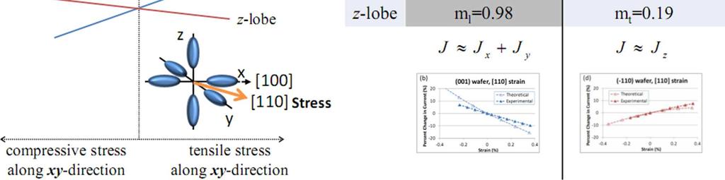
28 Strain Dependence of Tunneling in Vertical Silicon Tunnel Diodes Objective: To determine the relative change in tunneling current due to applied uniaxial stress. Procedure:Experimentally measure the uniaxiallystressed vertical Si tunnel diodes and compare results to theoretical calculations. Tunneling Current Mechanically Applied Uniaxial Stress Vertical tunnel diodes were fabricated on (100), (110), and (111) Si substrates to study tunneling along these directions. The uniaxial bending apparatus was designed by the S. Thompson group at University of Florida. 28
29 Current (A) 1.E-04 1.E-05 1.E-06 1.E-07 1.E-08 1.E-09 1.E-10 1.E-11 1.E-12 1.E-13 1.E-14 IV Plot for (001) Wafer with [100] Stress Thermal Regime (63mV/decade) Trap Limited Regime Tunneling Regime Voltage on N-Region (Volts) Forward Bias z Tunneling Current y x 3.E-08 2.E-08 1.E-08 [100] [110] Uniaxial Stress Compressive Strain Tensile Strain Reverse Bias 29
30 20 Relative Change in Current Compared to 0% Strain (001) Wafer with [100] Stress 15 Percent Change in Current Compared to 0% Strain Case Increasing Compressive Strain Increasing Tensile Strain -0.13% Strain % Strain 0% Strain 0% Strain (remeasured) 0% Strain (remeasured 2) 0.065% Strain 0.13% Strain 0.195% Strain 0.195% Strain (remeasured) 0.26% Strain 0.325% Strain 0.39% Strain Voltage on N-Region (Volts) 30
31 Imaginary Band Structure Calculation for Silicon (001) Wafer with [100] stress Analysis of the action integral calculated using imaginary band structure shows that the stress dependence is most sensitive to changes in band edge energies and occupancy of the bands 3 Imaginary Band Structure of Silicon with [100] Uniaxial Strain 2.5 Imaginary k-vector (1/nm) SOH VB2 VB1 y-lobe Tunneling Action Integral x-lobe z-lobe T exp b a k x dx = exp b a k x de qf Energy (ev) 31
32 Theoretical Analysis Imaginary band structure calculations for (001) wafer with [100] stress showed a large sensitivity of the transmission probability to energy band edge movements with stress. Little change in tunneling mass Strained imaginary band structure data was not available for all wafer/strain configurations Ultimately, the theoretical calculations were made without imaginary band structure calculations, taking into account the changes in band edge energy and occupation of the different lobes. This produced a reasonable fit, since we compared changes in current with strain for a set tunneling direction. Different tunneling directions were not compared to each other. 32
33 Relative Change in Current with Applied Strain 33


34 Summary of the Tunneling Analysis 34
35 Summary Imaginary k-vector,, represents a decaying exponential wavefunction Imaginary band structure calculations allow for accurate calculation of the action integral Band edge effective mass is insufficient to capture tunneling in different directions Band structure calculations that incorporated strain matched the trending behavior of relative change in tunneling current vsstrain 35
 Jamie Teherani")

36 Acknowledgements DARPA Steep program IBM Network for Computational Nanotechnology (NCN) Jamie Teherani Collaborators: Paul Solomon (IBM), Mathieu Luisier(Purdue) Advisors: Judy Hoyt, DimitriAntoniadis Acknowledgements: Steve Laux(IBM) 36
Band-to-band Tunneling in Silicon Diodes and Tunnel Transistors
 Band-to-band Tunneling in Silicon Diodes and Tunnel Transistors by James Towfik Teherani B.S. Electrical Engineering The University of Texas at Austin, 2008 Submitted to the Department of Electrical Engineering
Analysis of Band-to-band. Tunneling Structures. Title of Talk. Dimitri Antoniadis and Judy Hoyt (PIs) Jamie Teherani and Tao Yu (Students) 8/21/2012
 Jamie Teherani and Tao Yu (Students) 8/21/2012") 1 Analysis of Band-to-band Title of Talk Tunneling Structures Dimitri Antoniadis and Judy Hoyt (PIs) Jamie Teherani and Tao Yu (Students) 8/21/2012 A Science & Technology Center Vertical Type-II TFET Structure
1 Analysis of Band-to-band Title of Talk Tunneling Structures Dimitri Antoniadis and Judy Hoyt (PIs) Jamie Teherani and Tao Yu (Students) 8/21/2012 A Science & Technology Center Vertical Type-II TFET Structure
Current mechanisms Exam January 27, 2012
 Current mechanisms Exam January 27, 2012 There are four mechanisms that typically cause currents to flow: thermionic emission, diffusion, drift, and tunneling. Explain briefly which kind of current mechanisms
Solid State Device Fundamentals
 Solid State Device Fundamentals ENS 345 Lecture Course by Alexander M. Zaitsev alexander.zaitsev@csi.cuny.edu Tel: 718 982 2812 Office 4N101b 1 Outline - Goals of the course. What is electronic device?
Part 5: Quantum Effects in MOS Devices
 Quantum Effects Lead to Phenomena such as: Ultra Thin Oxides Observe: High Leakage Currents Through the Oxide - Tunneling Depletion in Poly-Si metal gate capacitance effect Thickness of Inversion Layer
Scaling Issues in Planar FET: Dual Gate FET and FinFETs
 Scaling Issues in Planar FET: Dual Gate FET and FinFETs Lecture 12 Dr. Amr Bayoumi Fall 2014 Advanced Devices (EC760) Arab Academy for Science and Technology - Cairo 1 Outline Scaling Issues for Planar
Avalanche breakdown. Impact ionization causes an avalanche of current. Occurs at low doping
 Avalanche breakdown Impact ionization causes an avalanche of current Occurs at low doping Zener tunneling Electrons tunnel from valence band to conduction band Occurs at high doping Tunneling wave decays
High Mobility Materials and Novel Device Structures for High Performance Nanoscale MOSFETs
 High Mobility Materials and Novel Device Structures for High Performance Nanoscale MOSFETs Prof. (Dr.) Tejas Krishnamohan Department of Electrical Engineering Stanford University, CA & Intel Corporation
Simulation of Schottky Barrier MOSFET s with a Coupled Quantum Injection/Monte Carlo Technique
 IEEE TRANSACTIONS ON ELECTRON DEVICES, VOL. 47, NO. 6, JUNE 2000 1241 Simulation of Schottky Barrier MOSFET s with a Coupled Quantum Injection/Monte Carlo Technique Brian Winstead and Umberto Ravaioli,
Semiconductor Physics fall 2012 problems
 Semiconductor Physics fall 2012 problems 1. An n-type sample of silicon has a uniform density N D = 10 16 atoms cm -3 of arsenic, and a p-type silicon sample has N A = 10 15 atoms cm -3 of boron. For each
Multiple Gate CMOS and Beyond
 Multiple CMOS and Beyond Dept. of EECS, KAIST Yang-Kyu Choi Outline 1. Ultimate Scaling of MOSFETs - 3nm Nanowire FET - 8nm Non-Volatile Memory Device 2. Multiple Functions of MOSFETs 3. Summary 2 CMOS
Lecture 9. Strained-Si Technology I: Device Physics
 Strain Analysis in Daily Life Lecture 9 Strained-Si Technology I: Device Physics Background Planar MOSFETs FinFETs Reading: Y. Sun, S. Thompson, T. Nishida, Strain Effects in Semiconductors, Springer,
UNIVERSITY OF CALIFORNIA College of Engineering Department of Electrical Engineering and Computer Sciences. EECS 130 Professor Ali Javey Fall 2006
 UNIVERSITY OF CALIFORNIA College of Engineering Department of Electrical Engineering and Computer Sciences EECS 130 Professor Ali Javey Fall 2006 Midterm 2 Name: SID: Closed book. Two sheets of notes are
Quantum and Non-local Transport Models in Crosslight Device Simulators. Copyright 2008 Crosslight Software Inc.
 Quantum and Non-local Transport Models in Crosslight Device Simulators Copyright 2008 Crosslight Software Inc. 1 Introduction Quantization effects Content Self-consistent charge-potential profile. Space
Tunnel-FET: bridging the gap between prediction and experiment through calibration
 Tunnel-FET: bridging the gap between prediction and experiment through calibration Anne Verhulst Quentin Smets, Jasper Bizindavyi, Mazhar Mohammed, Devin Verreck, Salim El Kazzi, Alireza Alian, Yves Mols,
Semiconductor Physics and Devices
 The pn Junction 1) Charge carriers crossing the junction. 3) Barrier potential Semiconductor Physics and Devices Chapter 8. The pn Junction Diode 2) Formation of positive and negative ions. 4) Formation
8. Schottky contacts / JFETs
 Technische Universität Graz Institute of Solid State Physics 8. Schottky contacts / JFETs Nov. 21, 2018 Technische Universität Graz Institute of Solid State Physics metal - semiconductor contacts Photoelectric
OMEN an atomistic and full-band quantum transport simulator for post-cmos nanodevices
 Purdue University Purdue e-pubs Other Nanotechnology Publications Birck Nanotechnology Center 8-18-28 OMEN an atomistic and full-band quantum transport simulator for post-cmos nanodevices Mathieu Luisier
Quantum Phenomena & Nanotechnology (4B5)
") Quantum Phenomena & Nanotechnology (4B5) The 2-dimensional electron gas (2DEG), Resonant Tunneling diodes, Hot electron transistors Lecture 11 In this lecture, we are going to look at 2-dimensional electron
Quantum Phenomena & Nanotechnology (4B5) The 2-dimensional electron gas (2DEG), Resonant Tunneling diodes, Hot electron transistors Lecture 11 In this lecture, we are going to look at 2-dimensional electron
EECS130 Integrated Circuit Devices
 EECS130 Integrated Circuit Devices Professor Ali Javey 10/02/2007 MS Junctions, Lecture 2 MOS Cap, Lecture 1 Reading: finish chapter14, start chapter16 Announcements Professor Javey will hold his OH at
Schottky diodes. JFETs - MESFETs - MODFETs
 Technische Universität Graz Institute of Solid State Physics Schottky diodes JFETs - MESFETs - MODFETs Quasi Fermi level When the charge carriers are not in equilibrium the Fermi energy can be different
Solid State Device Fundamentals
 Solid State Device Fundamentals ENS 345 Lecture Course by Alexander M. Zaitsev alexander.zaitsev@csi.cuny.edu Tel: 718 982 2812 Office 4N101b 1 Outline - Goals of the course. What is electronic device?
MSE 310/ECE 340: Electrical Properties of Materials Fall 2014 Department of Materials Science and Engineering Boise State University
 MSE 310/ECE 340: Electrical Properties of Materials Fall 2014 Department of Materials Science and Engineering Boise State University Practice Final Exam 1 Read the questions carefully Label all figures
Analysis of InAs Vertical and Lateral Band-to-Band Tunneling. Transistors: Leveraging Vertical Tunneling for Improved Performance
 Analysis of InAs Vertical and Lateral Band-to-Band Tunneling Transistors: Leveraging Vertical Tunneling for Improved Performance Kartik Ganapathi, Youngki Yoon and Sayeef Salahuddin a) Department of Electrical
MODELLING OF TUNNELLING CURRENTS IN METAL-INSULATOR-METAL JUNCTION
 MODELLING OF TUNNELLING CURRENTS IN METAL-INSULATOR-METAL JUNCTION ABSTRACT Ajay Manwani 1, Rajesh Junghare 2 and Abhishek Vaidya 3 Visvesvarya National Institute of Technology, Nagpur, India A numerical
MOS Capacitor MOSFET Devices. MOSFET s. INEL Solid State Electronics. Manuel Toledo Quiñones. ECE Dept. UPRM.
 INEL 6055 - Solid State Electronics ECE Dept. UPRM 20th March 2006 Definitions MOS Capacitor Isolated Metal, SiO 2, Si Threshold Voltage qφ m metal d vacuum level SiO qχ 2 E g /2 qφ F E C E i E F E v qφ
Overview of Modeling and Simulation TCAD - FLOOPS / FLOODS
 Overview of Modeling and Simulation TCAD - FLOOPS / FLOODS Modeling Overview Strain Effects Thermal Modeling TCAD Modeling Outline FLOOPS / FLOODS Introduction Progress on GaN Devices Prospects for Reliability
Subthreshold and scaling of PtSi Schottky barrier MOSFETs
 Superlattices and Microstructures, Vol. 28, No. 5/6, 2000 doi:10.1006/spmi.2000.0954 Available online at http://www.idealibrary.com on Subthreshold and scaling of PtSi Schottky barrier MOSFETs L. E. CALVET,
Surfaces, Interfaces, and Layered Devices
 Surfaces, Interfaces, and Layered Devices Building blocks for nanodevices! W. Pauli: God made solids, but surfaces were the work of Devil. Surfaces and Interfaces 1 Interface between a crystal and vacuum
An Analytical Model for a Gate-Induced-Drain-Leakage Current in a Buried-Channel PMOSFET
 Journal of the Korean Physical Society, Vol. 4, No. 5, November 00, pp. 86 867 An Analytical Model for a Gate-Induced-Drain-Leakage Current in a Buried-Channel PMOSFET Seong-Ho Kim, Sung-Eun Kim, Joo-Han
Suppression of Gate-Induced Drain Leakage by Optimization of Junction Profiles in 22 nm and 32 nm SOI nfets
 Suppression of Gate-Induced Drain Leakage by Optimization of Junction Profiles in 22 nm and 32 nm SOI nfets Andreas Schenk a,, a Integrated Systems Laboratory, ETH Zurich, Gloriastrasse 35, CH-8092, Switzerland
Long Channel MOS Transistors
 Long Channel MOS Transistors The theory developed for MOS capacitor (HO #2) can be directly extended to Metal-Oxide-Semiconductor Field-Effect transistors (MOSFET) by considering the following structure:
ECE-305: Fall 2017 Metal Oxide Semiconductor Devices
 C-305: Fall 2017 Metal Oxide Semiconductor Devices Pierret, Semiconductor Device Fundamentals (SDF) Chapters 15+16 (pp. 525-530, 563-599) Professor Peter Bermel lectrical and Computer ngineering Purdue
The Critical Role of Quantum Capacitance in Compact Modeling of Nano-Scaled and Nanoelectronic Devices
 The Critical Role of Quantum Capacitance in Compact Modeling of Nano-Scaled and Nanoelectronic Devices Zhiping Yu and Jinyu Zhang Institute of Microelectronics Tsinghua University, Beijing, China yuzhip@tsinghua.edu.cn
Modeling and Computation of Gate Tunneling Current through Ultra Thin Gate Oxides in Double Gate MOSFETs with Ultra Thin Body Silicon Channel
 Modeling and Computation of Gate Tunneling Current through Ultra Thin Gate Oxides in Double Gate MOSFETs with Ultra Thin Body Silicon Channel Bhadrinarayana L V 17 th July 2008 Microelectronics Lab, Indian
Physics of Semiconductors (Problems for report)
") Physics of Semiconductors (Problems for report) Shingo Katsumoto Institute for Solid State Physics, University of Tokyo July, 0 Choose two from the following eight problems and solve them. I. Fundamentals
Physics of Semiconductors (Problems for report) Shingo Katsumoto Institute for Solid State Physics, University of Tokyo July, 0 Choose two from the following eight problems and solve them. I. Fundamentals
Three-Dimensional Silicon-Germanium Nanostructures for Light Emitters and On-Chip Optical. Interconnects
 Three-Dimensional Silicon-Germanium Nanostructures for Light Emitters and On-Chip Optical eptember 2011 Interconnects Leonid Tsybeskov Department of Electrical and Computer Engineering New Jersey Institute
Semiconductor Physics Problems 2015
 Semiconductor Physics Problems 2015 Page and figure numbers refer to Semiconductor Devices Physics and Technology, 3rd edition, by SM Sze and M-K Lee 1. The purest semiconductor crystals it is possible
Schottky Rectifiers Zheng Yang (ERF 3017,
 ECE442 Power Semiconductor Devices and Integrated Circuits Schottky Rectifiers Zheng Yang (ERF 3017, email: yangzhen@uic.edu) Power Schottky Rectifier Structure 2 Metal-Semiconductor Contact The work function
ESE 570: Digital Integrated Circuits and VLSI Fundamentals
 ESE 570: Digital Integrated Circuits and VLSI Fundamentals Lec 4: January 23, 2018 MOS Transistor Theory, MOS Model Penn ESE 570 Spring 2018 Khanna Lecture Outline! CMOS Process Enhancements! Semiconductor
How a single defect can affect silicon nano-devices. Ted Thorbeck
 How a single defect can affect silicon nano-devices Ted Thorbeck tedt@nist.gov The Big Idea As MOS-FETs continue to shrink, single atomic scale defects are beginning to affect device performance Gate Source
Review Energy Bands Carrier Density & Mobility Carrier Transport Generation and Recombination
 Review Energy Bands Carrier Density & Mobility Carrier Transport Generation and Recombination The Metal-Semiconductor Junction: Review Energy band diagram of the metal and the semiconductor before (a)
Experimental and theoretical study of ultra-thin oxides
 Semicond. Sci. Technol. 13 (1998) A155 A159. Printed in the UK PII: S0268-1242(98)91837-5 Experimental and theoretical study of ultra-thin oxides E S Daniel, D Z-Y Ting and T C McGill T J Watson Sr Laboratory
Tunneling transport. Courtesy Prof. S. Sawyer, RPI Also Davies Ch. 5
 unneling transport Courtesy Prof. S. Sawyer, RPI Also Davies Ch. 5 Electron transport properties l e : electronic mean free path l φ : phase coherence length λ F : Fermi wavelength ecture Outline Important
ELEC 4700 Assignment #2
 ELEC 4700 Assignment #2 Question 1 (Kasop 4.2) Molecular Orbitals and Atomic Orbitals Consider a linear chain of four identical atoms representing a hypothetical molecule. Suppose that each atomic wavefunction
MOSFET: Introduction
 E&CE 437 Integrated VLSI Systems MOS Transistor 1 of 30 MOSFET: Introduction Metal oxide semiconductor field effect transistor (MOSFET) or MOS is widely used for implementing digital designs Its major
Supplementary Materials for
 advances.sciencemag.org/cgi/content/full/3/4/e1602726/dc1 Supplementary Materials for Selective control of electron and hole tunneling in 2D assembly This PDF file includes: Dongil Chu, Young Hee Lee,
Performance Analysis of Ultra-Scaled InAs HEMTs
 Purdue University Purdue e-pubs Birck and NCN Publications Birck Nanotechnology Center 2009 Performance Analysis of Ultra-Scaled InAs HEMTs Neerav Kharche Birck Nanotechnology Center and Purdue University,
Effect of Mechanical Stress on Gate Current and Degradation in AlGaN/GaN HEMTs
 Effect of Mechanical Stress on Gate Current and Degradation in AlGaN/GaN HEMTs Andrew Koehler, Min Chu, Amit Gupta, Mehmet Baykan, Scott Thompson, and Toshikazu Nishida Florida MURI Review November 10,
Development Software of Al-SiO 2 -Si MOS IV Characterization in Accumulation Case
 Applied Physics Research; Vol. 7, No. ; 015 ISSN 1916-9639 E-ISSN 1916-9647 Published by Canadian Center of Science and Education Development Software of -SiO -Si MOS IV Characteriation in Accumulation
Figure 3.1 (p. 141) Figure 3.2 (p. 142)
 Figure 3.2 (p. 142)") Figure 3.1 (p. 141) Allowed electronic-energy-state systems for two isolated materials. States marked with an X are filled; those unmarked are empty. System 1 is a qualitative representation of a metal;
Figure 3.1 (p. 141) Allowed electronic-energy-state systems for two isolated materials. States marked with an X are filled; those unmarked are empty. System 1 is a qualitative representation of a metal;
Impact of Silicon Wafer Orientation on the Performance of Metal Source/Drain MOSFET in Nanoscale Regime: a Numerical Study
 JNS 2 (2013) 477-483 Impact of Silicon Wafer Orientation on the Performance of Metal Source/Drain MOSFET in Nanoscale Regime: a Numerical Study Z. Ahangari *a, M. Fathipour b a Department of Electrical
A final review session will be offered on Thursday, May 10 from 10AM to 12noon in 521 Cory (the Hogan Room).
.") A final review session will be offered on Thursday, May 10 from 10AM to 12noon in 521 Cory (the Hogan Room). The Final Exam will take place from 12:30PM to 3:30PM on Saturday May 12 in 60 Evans.» All of
A final review session will be offered on Thursday, May 10 from 10AM to 12noon in 521 Cory (the Hogan Room). The Final Exam will take place from 12:30PM to 3:30PM on Saturday May 12 in 60 Evans.» All of
PHYSICAL ELECTRONICS(ECE3540) CHAPTER 9 METAL SEMICONDUCTOR AND SEMICONDUCTOR HETERO-JUNCTIONS
 CHAPTER 9 METAL SEMICONDUCTOR AND SEMICONDUCTOR HETERO-JUNCTIONS") PHYSICAL ELECTRONICS(ECE3540) CHAPTER 9 METAL SEMICONDUCTOR AND SEMICONDUCTOR HETERO-JUNCTIONS Tennessee Technological University Monday, November 11, 013 1 Introduction Chapter 4: we considered the semiconductor
PHYSICAL ELECTRONICS(ECE3540) CHAPTER 9 METAL SEMICONDUCTOR AND SEMICONDUCTOR HETERO-JUNCTIONS Tennessee Technological University Monday, November 11, 013 1 Introduction Chapter 4: we considered the semiconductor
Ultra-Scaled InAs HEMTs
 Performance Analysis of Ultra-Scaled InAs HEMTs Neerav Kharche 1, Gerhard Klimeck 1, Dae-Hyun Kim 2,3, Jesús. A. del Alamo 2, and Mathieu Luisier 1 1 Network for Computational ti Nanotechnology and Birck
Fundamentals of the Metal Oxide Semiconductor Field-Effect Transistor
 Triode Working FET Fundamentals of the Metal Oxide Semiconductor Field-Effect Transistor The characteristics of energy bands as a function of applied voltage. Surface inversion. The expression for the
Lecture 20: Semiconductor Structures Kittel Ch 17, p , extra material in the class notes
 Lecture 20: Semiconductor Structures Kittel Ch 17, p 494-503, 507-511 + extra material in the class notes MOS Structure Layer Structure metal Oxide insulator Semiconductor Semiconductor Large-gap Semiconductor
4.2 Molecular orbitals and atomic orbitals Consider a linear chain of four identical atoms representing a hypothetical molecule.
 4. Molecular orbitals and atomic orbitals Consider a linear chain of four identical atoms representing a hypothetical molecule. Suppose that each atomic wavefunction is 1s wavefunction. This system of
Energy position of the active near-interface traps in metal oxide semiconductor field-effect transistors on 4H SiC
 Energy position of the active near-interface traps in metal oxide semiconductor field-effect transistors on 4H SiC Author Haasmann, Daniel, Dimitrijev, Sima Published 2013 Journal Title Applied Physics
Lecture 6: 2D FET Electrostatics
 Lecture 6: 2D FET Electrostatics 2016-02-01 Lecture 6, High Speed Devices 2014 1 Lecture 6: III-V FET DC I - MESFETs Reading Guide: Liu: 323-337 (he mainly focuses on the single heterostructure FET) Jena:
Si - Based Tunnel Diode Operation and Forecasted Performance
 Si - Based Tunnel Diode Operation and Forecasted Performance Roger Lake Raytheon Systems Dallas, TX Si / Si x Ge -x Interband Tunnel Diodes The main tunneling process is LA and TO phonon assisted tunneling
MENA9510 characterization course: Capacitance-voltage (CV) measurements
 measurements") MENA9510 characterization course: Capacitance-voltage (CV) measurements 30.10.2017 Halvard Haug Outline Overview of interesting sample structures Ohmic and schottky contacts Why C-V for solar cells? The
MENA9510 characterization course: Capacitance-voltage (CV) measurements 30.10.2017 Halvard Haug Outline Overview of interesting sample structures Ohmic and schottky contacts Why C-V for solar cells? The
Nanoelectronics. Topics
 Nanoelectronics Topics Moore s Law Inorganic nanoelectronic devices Resonant tunneling Quantum dots Single electron transistors Motivation for molecular electronics The review article Overview of Nanoelectronic
Final Examination EE 130 December 16, 1997 Time allotted: 180 minutes
 Final Examination EE 130 December 16, 1997 Time allotted: 180 minutes Problem 1: Semiconductor Fundamentals [30 points] A uniformly doped silicon sample of length 100µm and cross-sectional area 100µm 2
This article has been accepted and published on J-STAGE in advance of copyediting. Content is final as presented.
 This article has been accepted and published on J-STAGE in advance of copyediting. Content is final as presented. References IEICE Electronics Express, Vol.* No.*,*-* Effects of Gamma-ray radiation on
A Multi-Gate CMOS Compact Model BSIMMG
 A Multi-Gate CMOS Compact Model BSIMMG Darsen Lu, Sriramkumar Venugopalan, Tanvir Morshed, Yogesh Singh Chauhan, Chung-Hsun Lin, Mohan Dunga, Ali Niknejad and Chenming Hu University of California, Berkeley
Problem 9.20 Threshold bias for an n-channel MOSFET: In the text we used a criterion that the inversion of the MOSFET channel occurs when V s = ;2 F w
 Prof. Jasprit Singh Fall 2001 EECS 320 Homework 11 The nals for this course are set for Friday December 14, 6:30 8:30 pm and Friday Dec. 21, 10:30 am 12:30 pm. Please choose one of these times and inform
Physics of Semiconductors
 Physics of Semiconductors 13 th 2016.7.11 Shingo Katsumoto Department of Physics and Institute for Solid State Physics University of Tokyo Outline today Laughlin s justification Spintronics Two current
Physics of Semiconductors
 Physics of Semiconductors 9 th 2016.6.13 Shingo Katsumoto Department of Physics and Institute for Solid State Physics University of Tokyo Site for uploading answer sheet Outline today Answer to the question
Modern physics. 4. Barriers and wells. Lectures in Physics, summer
 Modern physics 4. Barriers and wells Lectures in Physics, summer 016 1 Outline 4.1. Particle motion in the presence of a potential barrier 4.. Wave functions in the presence of a potential barrier 4.3.
Nanoscience and Molecular Engineering (ChemE 498A) Semiconductor Nano Devices
 Semiconductor Nano Devices") Reading: The first two readings cover the questions to bands and quasi-electrons/holes. See also problem 4. General Questions: 1. What is the main difference between a metal and a semiconductor or insulator,
Reading: The first two readings cover the questions to bands and quasi-electrons/holes. See also problem 4. General Questions: 1. What is the main difference between a metal and a semiconductor or insulator,
Chapter 7. The pn Junction
 Chapter 7 The pn Junction Chapter 7 PN Junction PN junction can be fabricated by implanting or diffusing donors into a P-type substrate such that a layer of semiconductor is converted into N type. Converting
ESE 570: Digital Integrated Circuits and VLSI Fundamentals
 ESE 570: Digital Integrated Circuits and VLSI Fundamentals Lec 4: January 29, 2019 MOS Transistor Theory, MOS Model Penn ESE 570 Spring 2019 Khanna Lecture Outline! CMOS Process Enhancements! Semiconductor
Modeling Electron Emission From Diamond-Amplified Cathodes
 Modeling Electron Emission From Diamond-Amplified Cathodes D. A. Dimitrov Tech-X Corporation, Boulder, CO I. Ben-Zvi, T. Rao, J. Smedley, E. Wang, X. Chang Brookhaven National Lab, NY This work is funded
PHYSICAL ELECTRONICS(ECE3540) CHAPTER 9 METAL SEMICONDUCTOR AND SEMICONDUCTOR HETERO-JUNCTIONS
 CHAPTER 9 METAL SEMICONDUCTOR AND SEMICONDUCTOR HETERO-JUNCTIONS") PHYSICAL ELECTRONICS(ECE3540) CHAPTER 9 METAL SEMICONDUCTOR AND SEMICONDUCTOR HETERO-JUNCTIONS Tennessee Technological University Wednesday, October 30, 013 1 Introduction Chapter 4: we considered the
PHYSICAL ELECTRONICS(ECE3540) CHAPTER 9 METAL SEMICONDUCTOR AND SEMICONDUCTOR HETERO-JUNCTIONS Tennessee Technological University Wednesday, October 30, 013 1 Introduction Chapter 4: we considered the
3. Two-dimensional systems
 3. Two-dimensional systems Image from IBM-Almaden 1 Introduction Type I: natural layered structures, e.g., graphite (with C nanostructures) Type II: artificial structures, heterojunctions Great technological
Ge Quantum Well Modulators on Si. D. A. B. Miller, R. K. Schaevitz, J. E. Roth, Shen Ren, and Onur Fidaner
 10.1149/1.2986844 The Electrochemical Society Ge Quantum Well Modulators on Si D. A. B. Miller, R. K. Schaevitz, J. E. Roth, Shen Ren, and Onur Fidaner Ginzton Laboratory, 450 Via Palou, Stanford CA 94305-4088,
ELEC 3908, Physical Electronics, Lecture 23. The MOSFET Square Law Model
 ELEC 3908, Physical Electronics, Lecture 23 The MOSFET Square Law Model Lecture Outline As with the diode and bipolar, have looked at basic structure of the MOSFET and now turn to derivation of a current
MOS CAPACITOR AND MOSFET
 EE336 Semiconductor Devices 1 MOS CAPACITOR AND MOSFET Dr. Mohammed M. Farag Ideal MOS Capacitor Semiconductor Devices Physics and Technology Chapter 5 EE336 Semiconductor Devices 2 MOS Capacitor Structure
NBTI and Spin Dependent Charge Pumping in 4H-SiC MOSFETs
 NBTI and Spin Dependent Charge Pumping in 4H-SiC MOSFETs Mark A. Anders, Patrick M. Lenahan, Pennsylvania State University Aivars Lelis, US Army Research Laboratory Energy Deviations from the resonance
EE130: Integrated Circuit Devices
 EE130: Integrated Circuit Devices (online at http://webcast.berkeley.edu) Instructor: Prof. Tsu-Jae King (tking@eecs.berkeley.edu) TA s: Marie Eyoum (meyoum@eecs.berkeley.edu) Alvaro Padilla (apadilla@eecs.berkeley.edu)
Semi-Conductor & Diodes
 Semi-Conductor & Diodes Semi-Conductor Some Quantum mechanics refresher Band theory in solids: Semiconductor, insulator and conductor Doping Diode p-n junction Diode types applications Introduction In
Lecture 5: CMOS Transistor Theory
 Lecture 5: CMOS Transistor Theory Slides courtesy of Deming Chen Slides based on the initial set from David Harris CMOS VLSI Design Outline q q q q q q q Introduction MOS Capacitor nmos I-V Characteristics
ECE 340 Lecture 39 : MOS Capacitor II
 ECE 340 Lecture 39 : MOS Capacitor II Class Outline: Effects of Real Surfaces Threshold Voltage MOS Capacitance-Voltage Analysis Things you should know when you leave Key Questions What are the effects
Make sure the exam paper has 9 pages (including cover page) + 3 pages of data for reference
 + 3 pages of data for reference") UNIVERSITY OF CALIFORNIA College of Engineering Department of Electrical Engineering and Computer Sciences Spring 2006 EE143 Midterm Exam #1 Family Name First name SID Signature Make sure the exam paper
UNIVERSITY OF CALIFORNIA College of Engineering Department of Electrical Engineering and Computer Sciences Spring 2006 EE143 Midterm Exam #1 Family Name First name SID Signature Make sure the exam paper
Analytical Modeling of Threshold Voltage for a. Biaxial Strained-Si-MOSFET
 Contemporary Engineering Sciences, Vol. 4, 2011, no. 6, 249 258 Analytical Modeling of Threshold Voltage for a Biaxial Strained-Si-MOSFET Amit Chaudhry Faculty of University Institute of Engineering and
Challenges in the introduction of Band to Band tunneling in semiclassical models for Tunnel-FETs. DIEGM - University of Udine, IU.
 Challenges in the introduction of Band to Band tunneling in semiclassical models for Tunnel-FETs, L.De Michielis*, M.Iellina and L.Selmi DIEGM - University of Udine, IU.NET *EPFL Outline Context Quantum
Courtesy of S. Salahuddin (UC Berkeley) Lecture 4
 Lecture 4") Courtesy of S. Salahuddin (UC Berkeley) Lecture 4 MOSFET Transport Issues semiconductor band structure quantum confinement effects low-field mobility and high-field saturation Reading: - M. Lundstrom,
Courtesy of S. Salahuddin (UC Berkeley) Lecture 4 MOSFET Transport Issues semiconductor band structure quantum confinement effects low-field mobility and high-field saturation Reading: - M. Lundstrom,
! CMOS Process Enhancements. ! Semiconductor Physics. " Band gaps. " Field Effects. ! MOS Physics. " Cut-off. " Depletion.
 ESE 570: Digital Integrated Circuits and VLSI Fundamentals Lec 4: January 3, 018 MOS Transistor Theory, MOS Model Lecture Outline! CMOS Process Enhancements! Semiconductor Physics " Band gaps " Field Effects!
Fermi Level Pinning at Electrical Metal Contacts. of Monolayer Molybdenum Dichalcogenides
 Supporting information Fermi Level Pinning at Electrical Metal Contacts of Monolayer Molybdenum Dichalcogenides Changsik Kim 1,, Inyong Moon 1,, Daeyeong Lee 1, Min Sup Choi 1, Faisal Ahmed 1,2, Seunggeol
The Future of CMOS. David Pulfrey. CHRONOLOGY of the FET. Lecture Lilienfeld s patent (BG FET) 1965 Commercialization (Fairchild)
 1965 Commercialization (Fairchild)") The Future of CMOS David Pulfrey 1 CHRONOLOGY of the FET 1933 Lilienfeld s patent (BG FET) 1965 Commercialization (Fairchild) 1991 The most abundant object made by mankind (C.T. Sah) 2003 The 10 nm FET
The Future of CMOS David Pulfrey 1 CHRONOLOGY of the FET 1933 Lilienfeld s patent (BG FET) 1965 Commercialization (Fairchild) 1991 The most abundant object made by mankind (C.T. Sah) 2003 The 10 nm FET
Components Research, TMG Intel Corporation *QinetiQ. Contact:
 1 High-Performance 4nm Gate Length InSb P-Channel Compressively Strained Quantum Well Field Effect Transistors for Low-Power (V CC =.5V) Logic Applications M. Radosavljevic,, T. Ashley*, A. Andreev*, S.
Reinventing the PN Junction: Dimensionality Effects on Tunneling Switches. Sapan Agarwal. A dissertation submitted in partial satisfaction of the
 Reinventing the PN Junction: Dimensionality Effects on Tunneling Switches By Sapan Agarwal A dissertation submitted in partial satisfaction of the requirements for the degree of Doctor of Philosophy in
Section 12: Intro to Devices
 Section 12: Intro to Devices Extensive reading materials on reserve, including Robert F. Pierret, Semiconductor Device Fundamentals Bond Model of Electrons and Holes Si Si Si Si Si Si Si Si Si Silicon
Semiconductor Physics and Devices
 EE321 Fall 2015 September 28, 2015 Semiconductor Physics and Devices Weiwen Zou ( 邹卫文 ) Ph.D., Associate Prof. State Key Lab of advanced optical communication systems and networks, Dept. of Electronic
Lecture 12: MOS Capacitors, transistors. Context
 Lecture 12: MOS Capacitors, transistors Context In the last lecture, we discussed PN diodes, and the depletion layer into semiconductor surfaces. Small signal models In this lecture, we will apply those
Electrostatics of Nanowire Transistors
 Electrostatics of Nanowire Transistors Jing Guo, Jing Wang, Eric Polizzi, Supriyo Datta and Mark Lundstrom School of Electrical and Computer Engineering Purdue University, West Lafayette, IN, 47907 ABSTRACTS
ESE 570: Digital Integrated Circuits and VLSI Fundamentals
 ESE 570: Digital Integrated Circuits and VLSI Fundamentals Lec 4: January 24, 2017 MOS Transistor Theory, MOS Model Penn ESE 570 Spring 2017 Khanna Lecture Outline! Semiconductor Physics " Band gaps "
Semiconductor Detectors are Ionization Chambers. Detection volume with electric field Energy deposited positive and negative charge pairs
 1 V. Semiconductor Detectors V.1. Principles Semiconductor Detectors are Ionization Chambers Detection volume with electric field Energy deposited positive and negative charge pairs Charges move in field
The relentless march of the MOSFET gate oxide thickness to zero
 Microelectronics Reliability 40 (2000) 557±562 www.elsevier.com/locate/microrel The relentless march of the MOSFET gate oxide thickness to zero G. Timp a, *, J. Bude a, F. Baumann a, K.K. Bourdelle a,