Summary of readout test of DSG prototype with IPA4 cold preamp. C. Cattadori, M. Bernabe-Heider, O. Chkvorets, K. Gusev, M.
|
|
|
- Molly Ward
- 5 years ago
- Views:
Transcription


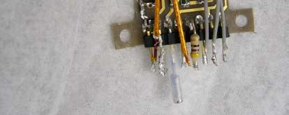

1 Summary of readout test of DSG prototype with IPA4 cold preamp C. Cattadori, M. Bernabe-Heider, O. Chkvorets, K. Gusev, M. Schircenko
2 Outline Summary of IPA4 circuit (see Nov06 Gerda meeting) The GERDA preamplifier based on IPA4 circuit Accessories for the cold read-out: HV connectors and cables. Summary of the tests performed with DSG prototype crystal in July-August 2006 in December January 2007.


 properly")

3 The tested setup (August 2006) The HV filter Solved problems of discharge on Ar side of HV feed-through due to proximity of HV to ground and low break-down of gas Ar. Solution: poor HV feed-through with Stycast 2850 FT (Dielectric Strength= 14 kv/mm) properly cured. Long test of connector and cable terminated with C (1nF,7.5 HV up to 4.5 kv The flange for cold CSA overnight OK.
 Weight ~ 3 g/m Assuming 10 mbq/kg (actual upper")
4 Adopted Cables for LARGE tests HV cable: Kapton coaxial cable. Tested up to 5 kv Weight ~ 3 g/m Signal: Kapton signal cable 50 W impedence at LAr (used in calorimetry) Weight ~ 3 g/m Assuming 10 mbq/kg (actual upper limit on γ- meas of Th and U on HV cable) 60 μbq from last meter of cable (nearest to electronic)
5 Equivalent circuit adopted to polarize detector and CSA readout + Shaper/FADC 12V HV 4k Cable T=300 K 1G 1G 1n 1n HV Filter Cable Cdet 30p T= 89 K RD 3,9k BF862 Noname + + R1 1G Cable IOP1 - - OP1!OPAMP Rf 1G Cf 500f Shaper T=300 K
6 Noise sources in the described chain Electronic noise originate: in the detector parallel or shot noise In the series resistance serial noise in the bias resistor 1/f noise dpn / df i = 2 e 2 n = 4kTR s i 2 = 4kT / nb R b 2 nf = Af / f e 2 n ei d HV 4k Rb 1G Cdet 30p Cb 1n Cs 1p Rs 50 RD 3,9k 12V BF862 Noname R1 1G Cable OP1!OPAMP - + IOP1 + eventually environmental noise -4.8 Rf 1G Cf 500f Shaper or FADC
7 going to numbers ( Q n / e) 2 = (2eI d + 4kT / Rb + i 2 na ) FT i p + (4kTR ( Q n s / e) e 2 [ 2 na pf ) F C v ns nv / T p 1 = 12[ ] I na ns d T F Parallel noise from detector LC p ] e / Hz 2 n vf A C T p f 2 C Parallel noise from bias R 5 kω T [ ] ns R p b +
8 Measuring the intrinsic resolution of a CSA 1 MeV released in Ge correspond to 54 fc MeV = (10 / 2.98) e = (10 / 2.98) C = 54 fc To inject the CSA inject the corresponding charge into FET through the test capacitance (Test Input) Qin = VinCt for Ct = 0.5 pf, Qin = 54 fc when Vin = 108mV To know intrinsic R of the CSA inject with pulser equivalent charge of 1.3 MeV and see FWHM of the peak appearing in spectra
9 Spectra obtained when doing intrinsic noise resolution: take position and FWHM of pulser line then do R
10 Before 28/07/2006: DSG crystal was working with Camberra warm CSA. HV=4000 V July-August 2006 test July-August 2006 test LC~ pa -> R@ Co ~ 4.2 kev(oleg confirm?) On 28/07/2006: Cold IPA4 preamp was mounted. Measurement of noise with capacitors Crystal connected HV=4000 V, LC~ 5000 pa Then reduce HV on crystal HV=3000 V R@ Co ~ 7 kev, R@Pulser = 6 kev 28/07/2006 On 28/07/2006 put back warm preamp but current high, noise, Crystal send to Camberra for reprocessing of dead layer
11 December January 2007 test Test of HV connector, cable filter without crystal Intrinsic resolution of the full chain measured with capacitor (cabling, mounting as with crsytal) 13/12/2006 Crystal connected to preamp mounted on cross
12 R [kev] Intrinsic Resolution of IPA4 cold CSA Shaping time [μs] Jul '06 Cd=0 in Lar, before connecting crystal Nov '06, final cabling EleLab, Cd=27 pf inlar Dec '06 in Large dewar, Cd=27 pf in LAr, HV OFF Dec '06 in Large dewar, Cd=27 pf in LAr, HV ON Jan '07 in Large dewar, Cd=100 pf in LAr, HV ON
13 Trend of meas LC and R of DSG crystal vs 4000V December I [pa] [kev] I Pulser /12/ /12/ /12/ /12/ /12/ /12/ /12/2006 Day
14 Peak Pos [ch] Co peak Pos and R from 22/12/2006 to 29/12/ Co Peak Pos Pulser R [kev] Best R obtained # file 1 file = 4 hours kev on pulser 4.1 kev on Co line
15
16 Test performed in January to study influence of cold CSA on the observed LC. Survey and Compare LC with PA On and OFF LC increase vs time after HV switch ON pa V, PA ON 3000 V, PA OFF hours
17 Study of the influence of cold CSA and HV filter on observed LC V-I curves to study CSA influence on LC [pa] jan-07 situation found after Xmass 16-jan-07 PA OFF, HV-F OUT 16-jan-07 PA ON, HV-F OUT 17-jan-07 New HV-F before pa, PA ON 18-jan-07 New HV-F before pa, PA ON [V]
18 last test to do: remove Crystal and test CSA cabled with HV C to simulate crystal R [kev] Intrinsic Resolution of IPA4 cold CSA Shaping time [μs] Jul '06 Cd=0 in Lar, before connecting crystal Nov '06, final cabling EleLab, Cd=27 pf inlar Dec '06 in Large dewar, Cd=27 pf in LAr, HV OFF Dec '06 in Large dewar, Cd=27 pf in LAr, HV ON Jan '07 in Large dewar, Cd=100 pf in LAr, HV ON Intrinsic noise of the PA is found to be consistent with the previous measurements, GERDA and meeting properly - Feb 07 - C. scales Cattadoriwith Cd
19 To measure crystal LC monitor the BL level shift Correlation between LC as measured on pa and BL shift of IPA4 Problem: BL shift [V] st repetition I [pa] nd repetition I (BL shift of IPA4) / I pa = 3 4. This possible only if 3 4 nominal value. Unconsistent with measured pulse reset time (800 ms). Need further check.
20 Comparison of measured resolution with measured LC Starting from the mentioned formula,1 na LC lead to a R degradation of 1.9 kev. R obtained never better than 4.1 kev (Co), and 3.5 kev (Pulser). R unconsistent with LC ( pa) noise pick up (observed noise at the scope@ 3 μs, not able to remove, but this noise is not present with Capacitor test with same cabling LV and HV PS, same mounting, same dewar ) 2 1 ( Q n / e) = 12[ ] I na ns = 1.9 kev for I d =1 na d T p
21 Conclusion IPA4 chip and CSA mounted around it are robust, never failed after >10 termic cycles. Bonding wire of the chip never break, PCB and chhosen components OK. Two test done connecting it with crystal, but high LC appeared both times Cold circuit connection not responsible for the increase of LC in crystal Measured resolution limited by LC (parallel noise) and HF noise observed Open issues Dedicated test bench to test electronic to reduce handling on crystal Source of HF noise
22 The IPA4 N-JFET N monolithic preamplifier Sensitivity A(f) g m J1 W,L of J1 ~ 2 V/pC with C f = 0.5 pf 108 mv/1 MeV in Ge 75 db 60 db (depending on the adopted configuration) 9.7 ma/v 1820 μm, 15 μm S f of J nv/hz 1/2 C i 9 pf τ r 400 ns with C f = 0.5 pf Output Single ended. Do not drive 50 Ω load. Power consumption ~ 100 mw Polarity positive and Negative V+,V- +12 V, -4.8 V
23 IPA4+external FET BF862: J1 (g m = 9.7 ma/v) is blocked and substituted by external BF862 (g m = 30 ma/v which can be kept at 0-60 cm from the CSA amplifying circuit IMPORTANT: With this modification τ f ~ ns in LAr External FET can be put on same or separate PCB
 for LNGS Phase I detector tests and MU 18 fold")

24 Production of 25 FE cryogenics circuits (based on IPA4 JFET monolithic circuit) for LNGS Phase I detector tests and MU 18 fold segmented prototype Production of PCB: 23 june at AREL, without 100 Ω output stage. PCB in DICLAD 880, 0.25 mm thick. Can be done in Kapton or PEN.
 IPA4 Chip in plastic SOIC14 case (MIPA4= 0.13 g) 9 HF pins for HF connection (Mpins = 0.")
25 The tested CSA PCB: DICLAD mm thick (MPCB= 0.57 g) IPA4 Chip in plastic SOIC14 case (MIPA4= 0.13 g) 9 HF pins for HF connection (Mpins = 0.45 g) CSA Based on IPA4. Total Mass = 1.7 g
26 July August 2006 tests: Intrinsic resolution of IPA4 CSA mounted on copper cross suspension with cabling etc. Measuring conditions as with crystal connected Shaping time [μs] FWHM E HV off [kev] Rel [%] Crystal disconnected CSA connected to flange through cables (70 cm long) PSA (semi-gaussion ORTEC mod. 572) + ADC +MCA Vin= 80 fc = 1.4 MeV Conclusion: Minimun of ENC found at 3 μs for CD = 27 pf, FWHM = MeV agreement with previous measurements
Pulse-shape shape analysis with a Broad-energy. Ge-detector. Marik Schönert. MPI für f r Kernphysik Heidelberg
 Pulse-shape shape analysis with a Broad-energy Ge-detector Marik Barnabé é Heider Dušan Budjáš Oleg Chkvorets Stefan Schönert MPI für f r Kernphysik Heidelberg Outline 1. Motivation and goals 2. BEGe detector
The GERDA Phase II detector assembly
 The GERDA Phase II detector assembly Tobias Bode 1, Carla Cattadori 2, Konstantin Gusev 1, Stefano Riboldi 2, Stefan Schönert 1, Bernhard Schwingenheuer 3 und Viktoria Wagner 3 for the GERDA collaboration
Status of the GERDA experiment
 Status of the GERDA experiment Hardy Simgen Max-Planck-Institute for Nuclear Physics Heidelberg The GERDA experiment Next generation 76 Ge double beta decay experiment at Gran Sasso. Basic idea: Operation
Now identified: Noise sources Amplifier components and basic design How to achieve best signal to noise?
 Signal processing Now identified: Noise sources Amplifier components and basic design How to achieve best signal to noise? Possible constraints power consumption ability to provide power & extract heat,
MSL/RAD Critical Design Review 7b RAD Sensor Head Stephan Böttcher
 MSL/RAD Critical Design Review 7b RAD Sensor Head Stephan Böttcher boettcher@physik.uni-kiel.de RAD Front-End-Electronics RAD Front-End-Electronics Functional Description Dynamic Range Requirement Photos
AGATA preamplifier performance on large signals from a 241 Am+Be source. F. Zocca, A. Pullia, D. Bazzacco, G. Pascovici
 AGATA preamplifier performance on large signals from a 241 Am+Be source F. Zocca, A. Pullia, D. Bazzacco, G. Pascovici AGATA Week - LNL (PD), Italy, 12-15 November 2007 Outline Recalls : Fast reset device
IH5341, IH5352. Dual SPST, Quad SPST CMOS RF/Video Switches. Description. Features. Ordering Information. Applications. Pinouts.
 SEMICONDUCTOR IH, IH2 December Features Description Dual SPST, Quad SPST CMOS RF/Video Switches R DS(ON) < Ω Switch Attenuation Varies Less Than db From DC to 00MHz "OFF" Isolation > 0dB Typical at 0MHz
ECE-342 Test 3: Nov 30, :00-8:00, Closed Book. Name : Solution
 ECE-342 Test 3: Nov 30, 2010 6:00-8:00, Closed Book Name : Solution All solutions must provide units as appropriate. Unless otherwise stated, assume T = 300 K. 1. (25 pts) Consider the amplifier shown
Acceptance test of the AGATA Ge detectors
 AGATA Week November 2007 Acceptance test of the AGATA Ge detectors University of Cologne Andreas Wiens B. Birkenbach, B. Bruyneel, J. Eberth, H. Hess, D. Lersch, G. Pascovici, P. Reiter - IKP Cologne H.-G.
Lecture 37: Frequency response. Context
 EECS 05 Spring 004, Lecture 37 Lecture 37: Frequency response Prof J. S. Smith EECS 05 Spring 004, Lecture 37 Context We will figure out more of the design parameters for the amplifier we looked at in
RANGE OF ALPHAS. Advanced Laboratory, Physics 407 University of Wisconsin Madison, Wisconsin 53706
 (revised 10/20/10) RANGE OF ALPHAS Advanced Laboratory, Physics 407 University of Wisconsin Madison, Wisconsin 53706 Abstract A silicon solid state detector is used to measure the energy of alphas which
arxiv: v1 [nucl-ex] 20 Dec 2008
![arxiv: v1 [nucl-ex] 20 Dec 2008](/thumbs/90/102022457.jpg "arxiv: v1 [nucl-ex] 20 Dec 2008") Operation of a GERDA Phase I prototype detector in liquid argon and nitrogen M. Barnabé Heider a, A. Bakalyarov b, L. Bezrukov c, C. Cattadori d, O. Chkvorets a, K. Gusev b,e, M. Hult f, I. Kirpichnikov
Operation of a GERDA Phase I prototype detector in liquid argon and nitrogen M. Barnabé Heider a, A. Bakalyarov b, L. Bezrukov c, C. Cattadori d, O. Chkvorets a, K. Gusev b,e, M. Hult f, I. Kirpichnikov
ECE-343 Test 1: Feb 10, :00-8:00pm, Closed Book. Name : SOLUTION
 ECE-343 Test : Feb 0, 00 6:00-8:00pm, Closed Book Name : SOLUTION C Depl = C J0 + V R /V o ) m C Diff = τ F g m ω T = g m C µ + C π ω T = g m I / D C GD + C or V OV GS b = τ i τ i = R i C i ω H b Z = Z
Study of a scintillation counter consisting of a pure CsI crystal and APD
 Study of a scintillation counter consisting of a pure CsI crystal and APD JIN Yifan Aihara Lab August 12th, 2015 1 Outline Belle II calorimeter upgrade Electronics noise in the scheme with APD CsI(pure)+(1-4)APDs
L4970A 10A SWITCHING REGULATOR
 L4970A 10A SWITCHING REGULATOR 10A OUTPUT CURRENT.1 TO 40 OUTPUT OLTAGE RANGE 0 TO 90 DUTY CYCLE RANGE INTERNAL FEED-FORWARD LINE REGULA- TION INTERNAL CURRENT LIMITING PRECISE.1 ± 2 ON CHIP REFERENCE
Study of pure CsI crystal coupling with APD. The University of Tokyo. Yi-Fan JIN
 Study of pure CsI crystal coupling with APD The University of Tokyo Yi-Fan JIN 1 BELLE II @ SuperKEKB High Energy Physics Experiment Electron-position collider Belle II Studies CP violation Using B mesons
MMIX4B12N300 V CES = 3000V. = 11A V CE(sat) 3.2V. High Voltage, High Gain BIMOSFET TM Monolithic Bipolar MOS Transistor
 3.2V. High Voltage, High Gain BIMOSFET TM Monolithic Bipolar MOS Transistor") High Voltage, High Gain BIMOSFET TM Monolithic Bipolar MOS Transistor Preliminary Technical Information V CES = 3V 11 = 11A V CE(sat) 3.2V C1 C2 (Electrically Isolated Tab) G1 E1C3 G2 E2C G3 G E3E C1 C2
High Voltage, High Gain BIMOSFET TM Monolithic Bipolar MOS Transistor Preliminary Technical Information V CES = 3V 11 = 11A V CE(sat) 3.2V C1 C2 (Electrically Isolated Tab) G1 E1C3 G2 E2C G3 G E3E C1 C2
ES51919/ES51920 LCR meter chipset
 ES51919/ES51920 LCR meter chipset Features 19,999/1,999 counts dual LCD display Application Handheld LCR bridge meter Current consumption: Typ. 25mA @ 100kHz QFP-100L package for ES51919 SSOP-48L package
ID # NAME. EE-255 EXAM 3 April 7, Instructor (circle one) Ogborn Lundstrom
 Ogborn Lundstrom") ID # NAME EE-255 EXAM 3 April 7, 1998 Instructor (circle one) Ogborn Lundstrom This exam consists of 20 multiple choice questions. Record all answers on this page, but you must turn in the entire exam.
ID # NAME EE-255 EXAM 3 April 7, 1998 Instructor (circle one) Ogborn Lundstrom This exam consists of 20 multiple choice questions. Record all answers on this page, but you must turn in the entire exam.
Switched-Capacitor Circuits David Johns and Ken Martin University of Toronto
 Switched-Capacitor Circuits David Johns and Ken Martin University of Toronto (johns@eecg.toronto.edu) (martin@eecg.toronto.edu) University of Toronto 1 of 60 Basic Building Blocks Opamps Ideal opamps usually
IXBT20N360HV IXBH20N360HV
 High Voltage, High Gain BIMOSFT TM Monolithic Bipolar MOS Transistor Advance Technical Information V CS = V = A V C(sat).V TO-HV (IXBT) Symbol Test Conditions Maximum Ratings V CS = C to C V V CGR = C
ESE 570: Digital Integrated Circuits and VLSI Fundamentals
 ESE 570: Digital Integrated Circuits and VLSI Fundamentals Lec 24: April 19, 2018 Crosstalk and Wiring, Transmission Lines Lecture Outline! Crosstalk! Repeaters in Wiring! Transmission Lines " Where transmission
MMIX4B22N300 V CES. = 3000V = 22A V CE(sat) 2.7V I C90
 2.7V I C90") Advance Technical Information High Voltage, High Gain BIMOSFET TM Monolithic Bipolar MOS Transistor (Electrically Isolated Tab) C G EC3 Symbol Test Conditions Maximum Ratings G3 C2 G2 E2C V CES = 25 C
Advance Technical Information High Voltage, High Gain BIMOSFET TM Monolithic Bipolar MOS Transistor (Electrically Isolated Tab) C G EC3 Symbol Test Conditions Maximum Ratings G3 C2 G2 E2C V CES = 25 C
Current feedback operational amplifiers as fast charge sensitive preamplifiers for
 Home Search Collections Journals About Contact us My IOPscience Current feedback operational amplifiers as fast charge sensitive preamplifiers for photomultiplier read out This article has been downloaded
DISCRETE SEMICONDUCTORS DATA SHEET. BLF246 VHF power MOS transistor Oct 21. Product specification Supersedes data of September 1992
 DISCRETE SEMICONDUCTORS DATA SHEET Supersedes data of September 1992 1996 Oct 21 FEATURES High power gain Low noise figure Easy power control Good thermal stability Withstands full load mismatch. PINNING
! Crosstalk. ! Repeaters in Wiring. ! Transmission Lines. " Where transmission lines arise? " Lossless Transmission Line.
 ESE 570: Digital Integrated Circuits and VLSI Fundamentals Lec 24: April 19, 2018 Crosstalk and Wiring, Transmission Lines Lecture Outline! Crosstalk! Repeaters in Wiring! Transmission Lines " Where transmission
MICROELECTRONIC CIRCUIT DESIGN Second Edition
 MICROELECTRONIC CIRCUIT DESIGN Second Edition Richard C. Jaeger and Travis N. Blalock Answers to Selected Problems Updated 10/23/06 Chapter 1 1.3 1.52 years, 5.06 years 1.5 2.00 years, 6.65 years 1.8 113
SWITCHED CAPACITOR AMPLIFIERS
 SWITCHED CAPACITOR AMPLIFIERS AO 0V 4. AO 0V 4.2 i Q AO 0V 4.3 Q AO 0V 4.4 Q i AO 0V 4.5 AO 0V 4.6 i Q AO 0V 4.7 Q AO 0V 4.8 i Q AO 0V 4.9 Simple amplifier First approach: A 0 = infinite. C : V C = V s
Prof. Anyes Taffard. Physics 120/220. Voltage Divider Capacitor RC circuits
 Prof. Anyes Taffard Physics 120/220 Voltage Divider Capacitor RC circuits Voltage Divider The figure is called a voltage divider. It s one of the most useful and important circuit elements we will encounter.
COURSE OUTLINE. Introduction Signals and Noise Filtering Sensors: Piezoelectric Force Sensors. Sensors, Signals and Noise 1
 Sensors, Signals and Noise 1 COURSE OUTLINE Introduction Signals and Noise Filtering Sensors: Piezoelectric Force Sensors Piezoelectric Force Sensors 2 Piezoelectric Effect and Materials Piezoelectric
Charge readout and double phase
 Charge readout and double phase Vyacheslav Galymov IPN Lyon 1 st annual meeting AIDA-2020 Liquid argon double-phase TPC Concept of double-phase LAr TPC (Not to scale) Anode 0V 2 mm Collection field 5kV/cm
Feedback Transimpedance & Current Amplifiers
 Feedback Transimpedance & Current Amplifiers Willy Sansen KULeuven, ESATMICAS Leuven, Belgium willy.sansen@esat.kuleuven.be Willy Sansen 1005 141 Table of contents Introduction Shuntshunt FB for Transimpedance
Homework Assignment 08
 Homework Assignment 08 Question 1 (Short Takes) Two points each unless otherwise indicated. 1. Give one phrase/sentence that describes the primary advantage of an active load. Answer: Large effective resistance
DISCRETE SEMICONDUCTORS DATA SHEET. BLW96 HF/VHF power transistor
 DISCRETE SEMICONDUCTORS DATA SHEET August 1986 DESCRIPTION N-P-N silicon planar epitaxial transistor intended for use in class-a, AB and B operated high power industrial and military transmitting equipment
ECE-343 Test 2: Mar 21, :00-8:00, Closed Book. Name : SOLUTION
 ECE-343 Test 2: Mar 21, 2012 6:00-8:00, Closed Book Name : SOLUTION 1. (25 pts) (a) Draw a circuit diagram for a differential amplifier designed under the following constraints: Use only BJTs. (You may
pickup from external sources unwanted feedback RF interference from system or elsewhere, power supply fluctuations ground currents
 Noise What is NOISE? A definition: Any unwanted signal obscuring signal to be observed two main origins EXTRINSIC NOISE examples... pickup from external sources unwanted feedback RF interference from system
Outline. Introduction, motivation Readout electronics, Peltier cooling Input J-FETsJ
 Progress in low energy X-rayX spectroscopy using semi-insulating insulating GaAs detectors F. Dubecký 1, B. Zaťko 1, P. Boháček 1, L. Ryć 2, E. Gombia 2, and V. Nečas 3 1 IEE SAS, Bratislava, Slovakia
AUTOMOTIVE CURRENT TRANSDUCER OPEN LOOP TECHNOLOGY HC6H 400-S/SP1
 AUTOMOTIVE CURRENT TRANSDUCER OPEN LOOP TECHNOLOGY HC6H 400-S/SP1 Picture of product with pencil Introduction The HC6H family is for the electronic measurement of DC, AC or pulsed currents in high power
DATA SHEET. BF245A; BF245B; BF245C N-channel silicon field-effect transistors DISCRETE SEMICONDUCTORS
 DISCRETE SEMICONDUCTORS DATA SHEET N-channel silicon field-effect transistors Supersedes data of April 995 File under Discrete Semiconductors, SC7 996 Jul FEATURES Interchangeability of drain and source
ECE 523/421 - Analog Electronics University of New Mexico Solutions Homework 3
 ECE 523/42 - Analog Electronics University of New Mexico Solutions Homework 3 Problem 7.90 Show that when ro is taken into account, the voltage gain of the source follower becomes G v v o v sig R L r o
Microelectronic Circuit Design 4th Edition Errata - Updated 4/4/14
 Chapter Text # Inside back cover: Triode region equation should not be squared! i D = K n v GS "V TN " v & DS % ( v DS $ 2 ' Page 49, first exercise, second answer: -1.35 x 10 6 cm/s Page 58, last exercise,
DISCRETE SEMICONDUCTORS DATA SHEET. BLW33 UHF linear power transistor
 DISCRETE SEMICONDUCTORS DATA SHEET August 1986 DESCRIPTION N-P-N silicon planar epitaxial transistor primarily intended for use in linear u.h.f. amplifiers for television transmitters and transposers.
Final Exam. 55:041 Electronic Circuits. The University of Iowa. Fall 2013.
 Final Exam Name: Max: 130 Points Question 1 In the circuit shown, the op-amp is ideal, except for an input bias current I b = 1 na. Further, R F = 10K, R 1 = 100 Ω and C = 1 μf. The switch is opened at
BFR93A. NPN Silicon RF Transistor. For low-noise, high-gain broadband amplifiers at collector currents from 2 ma to 30 ma
 NPN Silicon RF Transistor For lownoise, highgain broadband amplifiers at collector currents from ma to ma VPS5 ESD: Electrostatic discharge sensitive device, observe handling precaution! Type Marking Pin
5-V Low Drop Fixed Voltage Regulator TLE
 5-V Low Drop Fixed Voltage Regulator TLE 427-2 Features Output voltage tolerance ±2% 65 ma output current capability Low-drop voltage Reset functionality Adjustable reset time Suitable for use in automotive
HPGe detector fabrication at CANBERRA. V. Marian, M.O. Lampert, B. Pirard, P. Quirin, J. Flamanc CANBERRA Specialty Detectors (Lingolsheim)
") HPGe detector fabrication at CANBERRA V. Marian, M.O. Lampert, B. Pirard, P. Quirin, J. Flamanc CANBERRA Specialty Detectors (Lingolsheim) Ringberg Castle, October 2015 Outline CANBERRA Lingolsheim overview
HPGe detector fabrication at CANBERRA V. Marian, M.O. Lampert, B. Pirard, P. Quirin, J. Flamanc CANBERRA Specialty Detectors (Lingolsheim) Ringberg Castle, October 2015 Outline CANBERRA Lingolsheim overview
IXTF1N450 = 4500V. High Voltage Power MOSFET = 0.9A 80. R DS(on) (Electrically Isolated Tab) N-Channel Enhancement Mode.
 (Electrically Isolated Tab) N-Channel Enhancement Mode.") High Voltage Power MOSFET (Electrically Isolated Tab) S = 4500V I D25 = 0.9A 80 R DS(on) N-Channel Enhancement Mode ISOPLUS i4-pak TM Symbol Test Conditions Maximum Ratings S T J = 25 C to 50 C 4500 V
High Voltage Power MOSFET (Electrically Isolated Tab) S = 4500V I D25 = 0.9A 80 R DS(on) N-Channel Enhancement Mode ISOPLUS i4-pak TM Symbol Test Conditions Maximum Ratings S T J = 25 C to 50 C 4500 V
KH600. 1GHz, Differential Input/Output Amplifier. Features. Description. Applications. Typical Application
 KH 1GHz, Differential Input/Output Amplifier www.cadeka.com Features DC - 1GHz bandwidth Fixed 1dB (V/V) gain 1Ω (differential) inputs and outputs -7/-dBc nd/3rd HD at MHz ma output current 9V pp into
DISCRETE SEMICONDUCTORS DATA SHEET. BLF245 VHF power MOS transistor
 DISCRETE SEMICONDUCTORS DATA SHEET September 1992 FEATURES High power gain Low noise figure Easy power control Good thermal stability Withstands full load mismatch. DESCRIPTION Silicon N-channel enhancement
Advanced Current Mirrors and Opamps
 Advanced Current Mirrors and Opamps David Johns and Ken Martin (johns@eecg.toronto.edu) (martin@eecg.toronto.edu) slide 1 of 26 Wide-Swing Current Mirrors I bias I V I in out out = I in V W L bias ------------
Georgia Institute of Technology School of Electrical and Computer Engineering. Midterm-1 Exam (Solution)
") Georgia Institute of Technology School of Electrical and Computer Engineering Midterm-1 Exam (Solution) ECE-6414 Spring 2012 Friday, Feb. 17, 2012 Duration: 50min First name Solutions Last name Solutions
Georgia Institute of Technology School of Electrical and Computer Engineering Midterm-1 Exam (Solution) ECE-6414 Spring 2012 Friday, Feb. 17, 2012 Duration: 50min First name Solutions Last name Solutions
General Purpose Transistors
 General Purpose Transistors NPN and PNP Silicon These transistors are designed for general purpose amplifier applications. They are housed in the SOT 33/SC which is designed for low power surface mount
TYPE. max. working voltage 250 V 350 V 500 V 750 V. max. overload voltage 500 V 700 V 1000 V 1500 V. basic specifications IEC B
 FEATURES Non inductive High pulse loading capability. APPLICATIONS Application for overload and high voltage surge hazard circuits. DESCRIPTION A carbon film is deposited on a high grade ceramic body.
Characteristic of Capacitors
 3.5. The Effect of Non ideal Capacitors Characteristic of Capacitors 12 0 (db) 10 20 30 capacitor 0.001µF (1000pF) Chip monolithic 40 two-terminal ceramic capacitor 0.001µF (1000pF) 2.0 x 1.25 x 0.6 mm
1 of :32
 Home Page Products Price List Links & PDFs DISCONTINUED: SEE GAMMA-RAD Gamma Ray & X-Ray Spectroscopy System Hand-Held, High Efficiency NaI(Tl) Detector The GAMMA-8000 is a powerful, portable instrument
IXBT12N300 IXBH12N300
 High Voltage, High Gain BIMOSFET TM Monolithic Bipolar MOS Transistor S 11 = 3V = A (sat) 3.2V TO-26 (IXBT) Symbol Test Conditions Maximum Ratings S = 25 C to 15 C 3 V V CGR = 25 C to 15 C, R GE = 1MΩ
Lecture 18. New gas detectors Solid state trackers
 Lecture 18 New gas detectors Solid state trackers Time projection Chamber Full 3-D track reconstruction x-y from wires and segmented cathode of MWPC z from drift time de/dx information (extra) Drift over
AUTOMOTIVE CURRENT TRANSDUCER OPEN LOOP TECHNOLOGY HAH1BVW S/08
 AUTOMOTIVE CURRENT TRANSDUCER OPEN LOOP TECHNOLOGY HAH1BVW S/08 Introduction The HAH1BVW family is for the electronic measurement of DC, AC or pulsed currents in high power and low voltage automotive applications
PNP SILICON SWITCHING TRANSISTOR Qualified per MIL-PRF-19500/357
 DEVICES PNP SILICON SITCHING TRANSISTOR Qualified per MIL-PRF-19500/357 LEVELS 2N3634 2N3635 2N3636 2N3637 JAN 2N3634L 2N3635L 2N3636L 2N3637L JANTX 2N3634UB 2N3635UB 2N3636UB 2N3637UB JANTXV JANS ABSOLUTE
UNIT G485 Module Capacitors PRACTICE QUESTIONS (4)
") UNIT G485 Module 2 5.2.1 Capacitors PRACTICE QUESTIONS (4) 1 A 2200 µf capacitor is charged to a p.d. of 9.0 V and then discharged through a 100 kω resistor. (a) Calculate : (i) The initial charge stored
UNIT G485 Module 2 5.2.1 Capacitors PRACTICE QUESTIONS (4) 1 A 2200 µf capacitor is charged to a p.d. of 9.0 V and then discharged through a 100 kω resistor. (a) Calculate : (i) The initial charge stored
BEGe Detector studies update
 BEGe Detector studies update Performance and analysis Dušan Budjáš Stefan Schönert Mikael Hult* MPI für Kernphysik Heidelberg * IRMM Geel MAX-PLANCK-INSTITUTNSTITUT FÜR KERNPHYSIK Outline 1. BEGe publication
RP mA, Ultra-Low Noise, Ultra-Fast CMOS LDO Regulator. General Description. Features. Applications. Ordering Information. Marking Information
 RP122 3mA, Ultra-Low Noise, Ultra-Fast CMOS LDO Regulator General Description The RP122 is designed for portable RF and wireless applications with demanding performance and space requirements. The RP122
Preamplifier in 0.5µm CMOS
 A 2.125 Gbaud 1.6kΩ Transimpedance Preamplifier in 0.5µm CMOS Sunderarajan S. Mohan Thomas H. Lee Center for Integrated Systems Stanford University OUTLINE Motivation Shunt-peaked Amplifier Inductor Modeling
ORTEC AN34 Experiment 10 Compton Scattering
 EQUIPMENT NEEDED FROM ORTEC 113 Preamplifier (2 ea.) TRUMP-PCI-2K MCA System including suitable PC operating Windows 98/2000/XP (other ORTEC MCAs may be used) 266 Photomultiplier Tube Base (2 ea.) 4001A/4002D
Racal RA-117 Receiver Section: Notes, Layout, Tube List Page: 1 Dwg. Rev.: 2013 Jan 17
 Notes Early version retains the 0.- setting on RANGE, along with the accompanying L & C, from the RA-. Later version replaces this with the WIDEBAND Ω setting. Early version takes the socket (SK) off SK00
Amplifiers, Source followers & Cascodes
 Amplifiers, Source followers & Cascodes Willy Sansen KULeuven, ESAT-MICAS Leuven, Belgium willy.sansen@esat.kuleuven.be Willy Sansen 0-05 02 Operational amplifier Differential pair v- : B v + Current mirror
Grounding and Shielding
 Grounding and Shielding Veljko Radeka, BNL Outline Primary guidelines The Liquid Argon Calorimeter system Prevention of EMI and isolation Safety grounds Interface with other subsystems Status of implementation
Operational Field Coupled ESD Susceptibility of Magnetic Sensor IC s in Automotive Applications
 Operational Field Coupled ESD Susceptibility of Magnetic Sensor IC s in Automotive Applications *2014 IEEE International Symposium on Electromagnetic Compatibility, Raleigh, North Carolina Cyrous Rostamzadeh,
STUDIES ON LIGHTNING CHARACTERISTICS
 STUDIES ON LIGHTNING CHARACTERISTICS Lohit Singh.G 1, Piyush Kankariya 1, Rakesh Kumar 1, Varun.P 1, Shreyas 1, Madhu Palati 2 1 UG Student, 2 Assistant Professor, 1, 2 Department of Electrical & Electronics
DISCRETE SEMICONDUCTORS DATA SHEET M3D065. BLF245 VHF power MOS transistor. Product specification Supersedes data of 1997 Dec 17.
 DISCRETE SEMICONDUCTORS DATA SHEET M3D65 Supersedes data of 1997 Dec 17 23 Sep 2 FEATURES High power gain Low noise figure Easy power control Good thermal stability Withstands full load mismatch. DESCRIPTION
Understanding EMC Basics
 1of 7 series Webinar #1 of 3, February 27, 2013 EM field theory, and 3 types of EM analysis Webinar Sponsored by: EurIng CEng, FIET, Senior MIEEE, ACGI AR provides EMC solutions with our high power RF/Microwave
arxiv:nucl-ex/ v1 4 Jan 2007
 Characterization of the first true coaxial 18-fold segmented n-type prototype detector for the GERDA project arxiv:nucl-ex/07004v1 4 Jan 2007 Abstract I. Abt a, A. Caldwell a, D. Gutknecht b, K. Kröninger
Neutron Induced Nuclear Counter Effect in Hamamatsu Silicon APDs and PIN Diodes
 Neutron Induced Nuclear Counter Effect in Hamamatsu Silicon APDs and PIN Diodes Rihua Mao, Liyuan Zhang, Ren-yuan Zhu California Institute of Technology Introduction Because of its immunity to magnetic
Nuclear Lifetimes. = (Eq. 1) (Eq. 2)
 (Eq. 2)") Nuclear Lifetimes Theory The measurement of the lifetimes of excited nuclear states constitutes an important experimental technique in nuclear physics. The lifetime of a nuclear state is related to its
Nuclear Lifetimes Theory The measurement of the lifetimes of excited nuclear states constitutes an important experimental technique in nuclear physics. The lifetime of a nuclear state is related to its
Detection of γ-rays from nuclear decay: 0.1 < E γ < 20 MeV
 Detection of -rays from nuclear decay: 0.1 < < 0 MeV Basic concepts of radiation interaction & detection Compound Nucleus reactions and -ray emission High resolution detectors: the semiconductor Ge s Present
ORTEC. SLP Series Silicon Lithium-Drifted Planar Low-Energy X Ray Detector Product Configuration Guide
 ORTEC SLP Series Silicon Lithium-Drifted Planar Low-Energy Ray Detector For x-ray spectroscopy with a nuclear accelerator, radioactive source, or x-ray tube. Premium performance spectroscopy from 1 kev
Determining Characteristic Impedance and Velocity of Propagation by Measuring the Distributed Capacitance and Inductance of a Line
 Exercise 2-1 Determining Characteristic Impedance and Velocity EXERCISE OBJECTIVES Upon completion of this exercise, you will know how to measure the distributed capacitance and distributed inductance
TLF80511TF. Data Sheet. Automotive Power. Low Dropout Linear Fixed Voltage Regulator TLF80511TFV50 TLF80511TFV33. Rev. 1.
 Low Dropout Linear Fixed Voltage Regulator V50 V33 Data Sheet Rev. 1.0, 2014-01-28 Automotive Power Table of Contents 1 Overview....................................................................... 3
TOPFET high side switch
 DESCRIPTION QUICK REFERENCE DATA Monolithic temperature and SYMBOL PARAMETER MIN. UNIT overload protected power switch based on MOSFET technology in a I L Nominal load current (ISO) 9 A pin plastic envelope,
Generalized four-point characterization method for resistive and capacitive contacts
 Generalized four-point characterization method for resistive and capacitive contacts Brian S. Kim 1,a),b), Wang Zhou 1,a), Yash D. Shah 1,c), Chuanle Zhou 1, N. Işık 2,d), and M. Grayson 1,e) 1 Department
Features. Functional Diagrams, Pin Configurations, and Truth Tables
 Features Low On-Resistance (Ω typ) Minimizes Distortion and Error Voltages Low Glitching Reduces Step Errors in Sample-and-Holds. Charge Injection, pc typ Single-Supply Operation (+.V to +1V) Improved
CE/CS Amplifier Response at High Frequencies
 .. CE/CS Amplifier Response at High Frequencies INEL 4202 - Manuel Toledo August 20, 2012 INEL 4202 - Manuel Toledo CE/CS High Frequency Analysis 1/ 24 Outline.1 High Frequency Models.2 Simplified Method.3
EE105 Fall 2014 Microelectronic Devices and Circuits
 EE05 Fall 204 Microelectronic Devices and Circuits Prof. Ming C. Wu wu@eecs.berkeley.edu 5 Sutardja Dai Hall (SDH) Terminal Gain and I/O Resistances of BJT Amplifiers Emitter (CE) Collector (CC) Base (CB)
TLE Data Sheet. Automotive Power. Low Dropout Fixed Voltage Regulator TLE42644G. Rev. 1.1,
 Low Dropout Fixed Voltage Regulator TLE42644G Data Sheet Rev. 1.1, 214-7-3 Automotive Power Low Dropout Fixed Voltage Regulator TLE42644G 1 Overview Features Output Voltage 5 V ± 2 % up to Output Currents
Ref: HLSR 16-PW; HLSR 32-PW; HLSR 40-PW-000; HLSR 50-PW-000,
 Digital Current Transducer HLSR-PW series I P N = 16... 50 A Ref: HLSR 16-PW; HLSR 32-PW; HLSR 40-PW-000; HLSR 50-PW-000, Bitstream output from on onboard Sigma Delta modulator. For the electronic measurement
5-V Low Drop Fixed Voltage Regulator TLE 4275
 5-V Low Drop Fixed Voltage Regulator TLE 4275 Features Output voltage 5 V ± 2% Very low current consumption Power-on and undervoltage reset Reset low down to V Q = 1 V Very low-drop voltage Short-circuit-proof
Low Drift, Low Power Instrumentation Amplifier AD621
 a FEATURES EASY TO USE Pin-Strappable Gains of 0 and 00 All Errors Specified for Total System Performance Higher Performance than Discrete In Amp Designs Available in -Lead DIP and SOIC Low Power,.3 ma
For the electronic measurement of current: DC, AC, pulsed..., with galvanic separation between the primary and the secondary circuit.
 Current Transducer HO-NP series I P N = 4, 6, 12, 15 A Ref: HO 4-NP, HO 6-NP, HO 12-NP, HO 15-NP For the electronic measurement of current: DC, AC, pulsed..., with galvanic separation between the primary
5-V Low-Drop Fixed Voltage Regulator TLE 4269
 5-V Low-Drop Fixed Voltage Regulator TLE 4269 Features Output voltage tolerance ±2 % 15 ma current capability Very low current consumption Early warning Reset output low down to V Q = 1 V Overtemperature
THF / 1SCC330001M THF 1S1 C
 THF 2247 0191/ 1SCC330001M5803 34 THF 1S1 C Installation and Operation Instruction for THF Filter and Protective Unit THF 1_ THF 1S_ THF 1BS_ General guidelines Due to the fact that most UK building earth
Laboratory I: Impedance
 Physics 33, Fall 2008 ab I - Exercises aboratory I: Impedance eading: ab handout Simpson hapter if necessary) & hapter 2 particularly 2.9-2.3) ab Exercises. Part I What is the input impedance of the oscilloscope
Improved Quad CMOS Analog Switches
 Improved Quad CMOS Analog Switches DG211B, DG212B DESCRIPTION The DG211B, DG212B analog switches are highly improved versions of the industry-standard DG211, DG212. These devices are fabricated in proprietary
PPC Ge detectors for dark matter, neutrino-less double beta decay and CNS measurements
 PPC Ge detectors for dark matter, neutrino-less double beta decay and CNS measurements Ryan Martin, Queen s University Coherent Neutrino Scattering Experiment Workshop, Texas A&M 12 November 2015 R. Martin,
Dual Low Dropout Voltage Regulator
 Dual Low Dropout Voltage Regulator TLE 4473 GV55-2 Features Stand-by output 190 ma; 5 V ± 2% Main output: 300 ma, 5 V tracked to the stand-by output Low quiescent current consumption Disable function separately
CD4511BC BCD-to-7 Segment Latch/Decoder/Driver
 CD4511BC BCD-to-7 Segment Latch/Decoder/Driver General Description The CD4511BC BCD-to-seven segment latch/decoder/ driver is constructed with complementary MOS (CMOS) enhancement mode devices and NPN
A LDO Regulator with Weighted Current Feedback Technique for 0.47nF-10nF Capacitive Load
 A LDO Regulator with Weighted Current Feedback Technique for 0.47nF-10nF Capacitive Load Presented by Tan Xiao Liang Supervisor: A/P Chan Pak Kwong School of Electrical and Electronic Engineering 1 Outline
For the electronic measurement of current: DC, AC, pulsed..., with galvanic separation between the primary and the secondary circuit.
 Current Transducer LDSR 0.3-TP/SP1 I P R N = 300 ma For the electronic measurement of current: DC, AC, pulsed..., with galvanic separation between the primary and the secondary circuit. Features Closed
TLF80511EJ. Data Sheet. Automotive Power. Low Dropout Linear Fixed Voltage Regulator TLF80511EJV50 TLF80511EJV33. Rev. 1.
 Low Dropout Linear Fixed Voltage Regulator TLF80511EJV50 TLF80511EJV33 Data Sheet Rev. 1.0, 2014-11-17 Automotive Power Table of Contents 1 Overview.......................................................................
5-V Low Drop Fixed Voltage Regulator TLE 4299
 5-V Low Drop Fixed Voltage Regulator TLE 4299 Features Output voltage 5 V ± 2% 150 ma Output current Extreme low current consumption typical 65 µa in ON state Inhibit function: Below 1 µa current consumption
Miniature Electronically Trimmable Capacitor V DD. Maxim Integrated Products 1
 19-1948; Rev 1; 3/01 Miniature Electronically Trimmable Capacitor General Description The is a fine-line (geometry) electronically trimmable capacitor (FLECAP) programmable through a simple digital interface.