ESE 570: Digital Integrated Circuits and VLSI Fundamentals
|
|
|
- Moris Robertson
- 5 years ago
- Views:
Transcription
1 ESE 570: Digital Integrated Circuits and VLSI Fundamentals Lec 24: April 19, 2018 Crosstalk and Wiring, Transmission Lines
2 Lecture Outline! Crosstalk! Repeaters in Wiring! Transmission Lines " Where transmission lines arise? " Lossless Transmission Line " Termination " Lossy Transmission Line 2
3 Crosstalk 3
4 Capacitance! There are capacitors everywhere! Already talked about " Wires modeled as a distributed RC network " Parasitic capacitances between terminals on transistor 4
5 Capacitance Everywhere! Potentially a capacitor between any two conductors " On the chip " On the package " On the board! All wires " Package pins " PCB traces " Cable wires " Bit/word lines 5
6 Capacitance! decrease with conductor separation! increase with size! depends on dielectric C = ε r ε 0 A d 6
7 Wire Capacitance! Changes in voltage on one wire may couple through parasitic capacitance to an adjacent wire 7
8 Crosstalk! A capacitor does not like to change its voltage instantaneously! A wire has high capacitance to its neighbor. " When the neighbor switches from 1-> 0 or 0->1, the wire tends to switch too. " Called capacitive coupling or crosstalk.! Crosstalk effects " Noise on nonswitching wires " Increased delay on switching wires Slide 8
9 Qualitative
10 Driven Wire! What happens to a driven neighbor wire? " One wire switches " Neighbors driven but not switch " What happens to neighbors? 10
11 Driven Wire! Can this be a problem?! What if neighbor is: " Clock line " Asynchronous control " Non-clock used in synchronous system " Outputs sampled at clock edge 11
12 Undriven Wire! What happens to undriven wire?! Where do we have undriven wires? 12
13 Clocked Logic! CMOS driven lines! Clocked logic " Willing to wait to settle! Impact is on delay " May increase delay of transitions 13
14 Quantitative
15 Wire step response! Step response for isolated wire? 15
16 Undriven Adjacent Wire! V 1 transitions from 0 to V " How big is the noise on V 2? 16
17 Undriven Adjacent Wire! V 1 transitions from 0 to V " How big is the noise on V 2? I(t) = C dv(t) dt 17
18 Undriven Adjacent Wire! V 1 transitions from 0 to V " How big is the noise on V 2? I(t) = C dv(t) dt d(v C 1 (t) V 2 (t)) 1 dt dv C 1 (t) 1 = C 2 dv 2 (t) dt = (C 1 + C 2 ) dv (t) 2 dt dt C 1 V 1 (t) = (C 1 + C 2 )V 2 (t) V 2 (t) = C 1 C 1 + C 2 V 1 (t) 18
19 SPICE C 1 =10pF, C 2 =20pF 19
20 Good (?) Capacitance! High capacitance to ground plane " Limits node swing from adjacent conductors V 2 = " C $ 1 # C + C 1 2 % ' V & 1 20
21 Driven Adjacent Wire! What happens when neighbor line is driven? 21
22 Driven Adjacent Wire! What happens when neighbor line is driven? " Recovers with time constant: R 2 (C 1 +C 2 ) 22
23 Spice: R 2 =1K, C 1 =10pF, C 2 =20pF diversion 23
24 Magnitude of Noise on Driven Line! Magnitude of diversion depends on relative time constants " τ 1 << τ 2 " full diversion, then recover " τ 1 >> τ 2 " Drive capacitor faster than line 1 can change " τ 1 ~= τ 2 " little noise " Somewhere in between 24
25 Spice: C 1 =1pF, C 2 =2pF 25
26 Switching Line with Finite Drive! What impact does the presence of the non switching line have on the switching line? " All previous questions were about non-switching " Note R on switching 26
27 Simultaneous Transition! What happens if lines transition in opposite directions? 27
28 Simultaneous Transition! What happens if transition in opposite directions? " Must charge C 1 by 2V " Or looks like 2C 1 between wires 28
29 Simultaneous Transition! What happens if lines transition in same direction? 29
30 Simulation! V 2 switching at ¼ frequency of V 1! No crosstalk reference case where no V 2 30
31 Simulation Setup V1 V2 C1 C2 C2 31
32 Crosstalk Simulation 1.3ns 1.8ns 2.8ns 32
33 Crosstalk Simulation 1.3ns 1.8ns 2.8ns 33
34 Crosstalk Simulation 1.3ns 1.8ns 2.8ns 34
35 Where Does it Arise? 35

36 Cables and PCB Wires Source; 36

37 Printed Circuit Board Source: 37
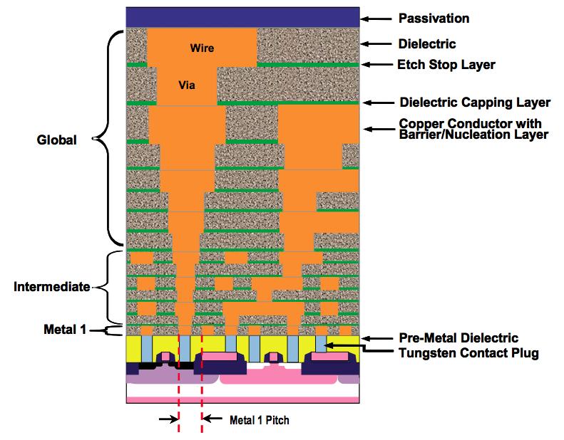
38 Interconnect Cross Section 38


39 Standard Cell Area inv nand3 All cells uniform height Cell area Width of channel determined by routing Penn ESE 570 Spring Khanna 39
40 Noise Implications! So what if we have noise?! If the noise is less than the noise margin, nothing happens! Static CMOS logic will eventually settle to correct output even if disturbed by large noise spikes " But glitches cause extra delay " Also cause extra power from false transitions! Dynamic logic never recovers from glitches " Can t correct mid-cycle, need precharge! Memories and other sensitive circuits also can produce the wrong result (i.e faults) Slide 40
41 Wire Engineering! Goal: achieve delay, area, power goals with acceptable noise! Degrees of freedom: Slide 41
42 Wire Engineering! Goal: achieve delay, area, power goals with acceptable noise! Degrees of freedom: " Width " Spacing " Layer w Delay (ns): RC/ s Pitch (nm) Coupling: 2C adj / (2C adj +C gnd ) Pitch (nm) Wire Spacing (nm) l t h Slide 42
43 Wire Engineering! Goal: achieve delay, area, power goals with acceptable noise! Degrees of freedom: " Width " Spacing " Layer " Shielding Delay (ns): RC/ Pitch (nm) Coupling: 2C adj / (2C adj +C gnd ) Pitch (nm) Wire Spacing (nm) vdd a 0 a 1 gnd a 2 a 3 vdd vdd a 0 gnd a 1 vdd a 2 gnd a 0 b 0 a 1 b 1 a 2 b 2 Slide 43
44 Repeaters in Wiring
45 Reminder: Wire Delay! Wire N units long: =R unit *C unit *N 2 /2! With R wire = N R unit C wire = N C unit " R unit =1kΩ " C unit =1pF Penn ESE 570 Spring Khanna 45
46 Interconnect Buffering! RC (on-chip) Interconnect Buffering 46
47 Delay of Wire! Long Wire: 1mm! R u = 60K Ω per 1mm of wire! C u = 0.16 pf per 1mm of wire! Driven by buffer " R buf = 25K Ω " C self = 0.02 ff " C g = 0.01fF! Loaded by identical buffer 47
48 Formulate Delay Delay of buffer driving wire? 48
49 Formulate Delay Delay of buffer driving wire? R buf ( C self + C wire + C ) load + 0.5R wire C wire + R wire C load 49
50 Calculate Delay! C load =! R buf =! C self =! C wire =! R wire = R buf ( C self + C wire + C ) load + 0.5R wire C wire + R wire C load 50
51 Calculate Delay! C load = 2 C g =.02fF! R buf = 25K Ω! C self = 0.02fF! C wire = L*C u =.16pF! R wire = L*R u = 60K Ω R buf ( C self + C wire + C ) load + 0.5R wire C wire + R wire C load 51
52 Calculate Delay! C load = 2 C g =.02fF! R buf = 25K Ω! C self = 0.02fF 8.8ns! C wire = L*C u =.16pF! R wire = L*R u = 60K Ω R buf ( C self + C wire + C ) load + 0.5R wire C wire + R wire C load 4ns + 4.8ns +1.2ps 52
53 Buffering Wire 53
54 Buffering Wire: L/2! C load =! R buf =! C self =! C wire =! R wire = 54
55 Buffering Wire: L/2! C load = 2 C g =.02fF! R buf = 25K Ω! C self =.02fF! C wire = L/2*C u =.08pF! R wire = L/2*R u = 30K Ω 55
56 Buffering Wire: L/2! C load = 2 C g =.02fF! R buf = 25K Ω! C self =.02fF! C wire = L/2*C u =.08pF! R wire = L/2*R u = 30K Ω R buf ( C self + C wire + C ) load + 0.5R wire C wire + R wire C load 2ns +1.2ns +.6 ps = 3.2ns 56
57 Buffering Wire: L/2! C load = 2 C g =.02fF! R buf = 25K Ω! C self =.02fF 6.4ns! C wire = L/2*C u =.08pF! R wire = L/2*R u = 30K Ω R buf ( C self + C wire + C ) load + 0.5R wire C wire + R wire C load 2ns +1.2ns +.6 ps = 3.2ns 57
58 Buffering Wire: L/N Wire of Length Delay (ns) Number in 1mm Total Delay for 1mm (ns) 1 mm 8.8ns 1 8.8ns 0.5mm 3.2ns 2 6.4ns 0.1mm mm mm 1000 R buf ( C self + C wire + C ) load + 0.5R wire C wire + R wire C load 58
59 Buffering Wire: L/N Wire of Length Delay (ns) Number in 1mm (N) Total Delay for 1mm (ns) 1 mm 8.8ns 1 8.8ns 0.5mm 3.2ns 2 6.4ns 0.1mm 0.45ns ns 0.01 mm.041ns ns mm.005ns ns R buf ( C self + C wire + C ) load + 0.5R wire C wire + R wire C load 59
60 N Buffers! Delay Equation for N buffers? N R buf C self + C wire N +C load R wire N C wire N + R wire N C load 60
61 Minimize Delay! Minimize delay! Derivative with respect to N and solve for 0 N R buf ( C self +C ) load + R buf C wire N 0 = R ( buf C self +C ) load N 2 R wire C wire + R wire C load R wire C wire N = R buf 0.5R wire C wire ( C self +C ) load 61
62 Minimize Delay Equalizes delay in buffer and wire N = R buf 0.5R wire C wire C self + C load ( ) N R buf ( C self + C ) + R C + 0.5! load # 1 buf wire " N $ &R wire C wire + R wire C load % 62
63 Delay with Optimal N R buf 0.5R wire C wire C self + C load ( ) R buf ( C self + C load ) + R buf C wire R wire C wire R buf ( C self + C load )! # # " R buf ( C self + C load ) 0.5R wire C wire $ & & R C + R C wire wire wire load % ( ) + R buf C wire + 0.5R wire C wire ( R buf ( C self + C load )) + R wire C load 2 0.5R wire C ( wire R ( buf C self + C )) load + R buf C wire + R wire C load 63
64 Segment Length! R wire = L R unit! C wire = L C unit * L seg = L N # R N = 0.5% wire C wire % $ R buf C self + C load ( ) & ( ( ' * L seg # R N = L 0.5% u C u % $ R buf C self + C load ( ) = L " N = 2 R buf C self + C load $ # R u C u & ( ( ' ( ) % ' & 64
65 Optimal Segment Length! Delay scales linearly with distance once optimally buffered * L seg = L # N = 2 R buf C self + C % load % R u C $ u ( ) & ( ( ' # N = L 0.5% % $ R u C u ( ) R buf C self + C load & ( ( ' 65
66 Buffer Size?! How big should buffer be? " R buf = R un /W " C self = 2 W C dff = 2 W γ C g " C load = 2 W C g 66
67 Buffer Size?! How big should buffer be? " R buf = R un /W " C self = 2 W C dff = 2 W γ C g " C load = 2 W C g 2 0.5R wire C ( wire R ( buf C self + C )) load + R buf C wire + R wire C load! R 2 0.5R wire C un wire # W 2WC g 1+γ " ( ( )) $ & + R un % W C wire + R wire 2WC g 2 0.5R wire C ( wire 2R un C ( g 1+γ) ) + R un W C wire + R wire 2WC g 67
68 Implication on Buffer Size - W! R wire = L R unit! C wire = L C unit 2 0.5R wire C ( wire 2R un C ( g 1+γ) ) + R un W C + R 2WC wire wire g 0 = 2R wire C g R un C wire 1 W 2 W = R un C wire 2R wire C g =! # W independent of Length " Depends on technology R un C unit 2R unit C g 68
69 Delay at Optimum W 2 0.5R wire C ( wire 2R un C g ( 1+γ) ) + R un W C + R 2WC wire wire g 2 0.5R wire C ( wire 2R un C g ( 1+γ) ) + R un R un C wire 2R wire C g C wire + R wire 2 R un C wire 2R wire C g C g 2 0.5R wire C ( wire 2R un C g ( 1+γ) ) + R un C wire 2R wire C g + R un C wire 2R wire C g 2 0.5R wire C ( wire 2R un C g ( 1+γ) ) + 2 2R un C g C wire R wire 69
70 Delay at Optimum W! If γ=1 2 R wire C ( wire R un C g ( 1+1) ) + 2 2R un C g C wire R wire 2 2R un C g C wire R wire + 2 2R un C g C wire R wire 4 2R un C g C wire R wire! Optimal design equalizes all delays! 70
71 Where Transmission Lines Arise 71


72 Transmission Lines! Cable: coaxial! PCB " Strip line " Microstrip line! Twisted Pair (Cat5) 72
73 Transmission Lines! This is what wires/cables look like " Aren t an ideal equipotential " Signals do take time to propagate " Maintain shape of input signal " Within limits " Shape and topology of wiring effects how signals propagate! Need theory/model to support design " Reason about behavior " Understand what can cause noise " Engineer high performance/speed communication 73
74 Wire Formulation 74
75 Wires! In general, our wires have distributed R, L, C components 75
76 RC Wire! When R dominates L " We have the distributed RC Wires " Typical of on-chip wires in ICs 76
77 Lossless Transmission Line! When resistance is negligible " Have LC wire = Lossless Transmission Line " No energy dissipation (loss) through R s " More typical of Printed Circuit Board wires and bond wires 77
78 Intuitive: Lossless! Pulses travel as waves without distortion " (up to a characteristic frequency) 78
79 SPICE Simulation 79
80 Step Response SPICE 80
81 Pulse Response SPICE 81
82 Contrast RC Wire 82
83 Contrast 83
84 Model! Now voltage is a function of time and position " Position along wire distance from source! Want to get V(x,t) " And I(x,t) 84
85 Implication " Wave equation: " Solution: 2 V x = LC 2 V t V(x,t) = A + Be x wt " What is w? Be x wt = LCw 2 Be x wt w = 1 LC w is the rate of propogation 85
86 Propagation Rate in Example! L=1uH! C=1pF! What is w? w = 1 LC 86
87 Signal Propagation 87
88 Signal Propagation Delay linear in length 88
89 Contrast RC Wire RC wire delay quadratic in length.5r un C un N 2 89
90 Impedance! Transmission lines have a characteristic impedance Z 0 = L C 90
91 Infinite Lossless Transmission Line! Transmission line looks like resistive load Z 0 = L C Z 0! Input waveform travels down line at velocity " Without distortion w = 1 LC 91
92 Termination
93 End of Line! What happens at the end of the transmission line? 93
94 Analyze End of Line! Incident Wave, Reflected Wave, Transverse Wave 94
95 End of Line! What happens at the end of the transmission line? " Short Circuit, R=0 " Hint: what must happen in steady state? " Terminate with R=Z 0 " Open Circuit, R= 95
96 Reflection Reflection coefficient # R Z V 0 i % $ R + Z 0 & ( = V ' r 96
97 Analyze End of Line! V i +V r =V t " R Z V 0 % i $ ' = V r # R + Z 0 & " R Z V 0 % i $ ' = V t V i # R + Z 0 & " R Z V 0 % i $ +1' = V t # R + Z 0 & V i " 2R % $ ' = V t # R + Z 0 & Transmission coefficient 97
98 Open # R Z V 0 & i % ( = V $ R + Z r 0 ' 98
99 Terminate R=Z 0 # R Z V 0 & i % ( = V $ R + Z r 0 ' 99
100 Short # R Z V 0 & i % ( = V $ R + Z r 0 ' 100
101 Longer LC (open)! 40 Stages! L=100nH! C=1pF w = 1 LC = c 0 Stage delay? How long to propogate? ε r µ r! Drive with 2ns Pulse! No termination (open circuit) " What reflection do we expect? 101

102 Pulse Travel RC! V1,V3,V4,V5,V6 about 10 stages apart 102
103 Visualization! Matched Open Short 103
104 Back to Source 104
105 Back at Source?! What happens at source? " Depends on how it s terminated 105
106 R Z 0! What happens? " 75 Ω termination on 50 Ω line 106
107 Transmission Line Symbol! Specify delay of full Tline and characteristic impedance! Need reference 107
108 Simulation! For these, with direct drive from voltage source " Source looks like short circuit (not typical of CMOS) " Source cannot be changed 108
109 50Ω line, 75Ω termination # R Z V r = V 0 i % $ R + Z 0 & # 75 50& ( = V i % ( = 0.2V ' $ ' i 109
110 Source Series Termination! What happens here? 110
111 Simulation 111
112 Series Termination! R series = Z 0! Initial voltage divider " Half voltage pulse propogates down Tline! End of line open circuit " Sees single transition to full voltage (full reflection)! Reflection returns to source and sees termination R series = Z 0! No further reflections 112
113 CMOS Driver / Receiver! Driver: What does a CMOS driver look like at the source? " I d,sat 45nm, V dd =1V! Receiver: What does a CMOS inverter look like at the sink? 113
114 CMOS Driver! Driver: What does a CMOS driver look like at the source? " I d,sat 45nm, V dd =1V " Min size: " I drive =1200µA/µm*45nm=54µA " R out =V dd /I drive =18kΩ 114
115 CMOS Driver! Driver: What does a CMOS driver look like at the source? " I d,sat 45nm, V dd =1V " Min size: " I drive =1200µA/µm*45nm=54µA " R out =V dd /I drive =18kΩ " W=370 " I drive =1200µA/µm*45nm*370=20mA " R out =V dd /I drive =50Ω 115
116 CMOS Receiver! Receiver: What does a CMOS inverter look like at the sink? 116
117 Lossy Transmission Line! How do addition of R s change? " Concretely, discretely think about R=0.2Ω every meter on Z 0 =100Ω " what does each R do? 117
118 Lossy Transmission Line! Each R is a mismatched termination! Each R is a voltage divider " 2(R + Z ) V = V 0 t i $ #(R + Z ) + Z 0 0 " Z V = V 0 i+1 t $ # R + Z 0 % ' & % ' & 118
119 Lossy Transmission Line " 2(R + Z ) V = V 0 i+1 i $ #(R + Z ) + Z 0 0 %" ' $ &# Z 0 R + Z 0 % ' & "" 2(R + Z ) V = V $ 0 snk src $ ##(R + Z ) + Z 0 0 %" ' $ &# Z 0 R + Z 0 %% '' && N 119
120 Lossy Transmission Line! How long before drop voltage by half? R=0.2Ω every meter on Z 0 =100Ω "" 2(R + Z ) V = V $ 0 snk src $ ##(R + Z ) + Z 0 0 %" ' $ &# Z 0 R + Z 0 %% '' && N 120
121 Idea! Capacitance is everywhere, especially between adjacent wires, and will get noise from crosstalk " Clocked and driven wires " Slow down transitions " Undriven wires voltage changed " Can cause spurious/false transitions! Wire delay linear once buffered optimally " Optimal buffering equalizes delays " Buffer delay, Delay on wire between buffers, Delay of wire driving buffer! Transmission lines " high-speed " high throughput " long-distance signaling! Termination 121
122 Admin! Tania extra office hours " Monday 1-3pm! Tuesday (last) lecture " Details about final exam " Review for final exam 122
! Crosstalk. ! Repeaters in Wiring. ! Transmission Lines. " Where transmission lines arise? " Lossless Transmission Line.
 ESE 570: Digital Integrated Circuits and VLSI Fundamentals Lec 24: April 19, 2018 Crosstalk and Wiring, Transmission Lines Lecture Outline! Crosstalk! Repeaters in Wiring! Transmission Lines " Where transmission
Interconnects. Wire Resistance Wire Capacitance Wire RC Delay Crosstalk Wire Engineering Repeaters. ECE 261 James Morizio 1
 Interconnects Wire Resistance Wire Capacitance Wire RC Delay Crosstalk Wire Engineering Repeaters ECE 261 James Morizio 1 Introduction Chips are mostly made of wires called interconnect In stick diagram,
Interconnects. Introduction
 Interconnects Wire Resistance Wire Capacitance Wire RC Delay Crosstalk Wire Engineering Repeaters ECE 261 Krish Chakrabarty 1 Introduction Chips are mostly made of ires called interconnect In stick diagram,
ESE 570: Digital Integrated Circuits and VLSI Fundamentals
 ESE 570: Digital Integrated Circuits and VLSI Fundamentals Lec 23: April 17, 2018 I/O Circuits, Inductive Noise, CLK Generation Lecture Outline! Packaging! Variation and Testing! I/O Circuits! Inductive
ESE 570: Digital Integrated Circuits and VLSI Fundamentals
 ESE 570: Digital Integrated Circuits and VLSI Fundamentals Lec 23: April 13, 2017 Variation; I/O Circuits, Inductive Noise Lecture Outline! Design Quality " Variation! Packaging! Variation and Testing!
Announcements. EE141- Fall 2002 Lecture 25. Interconnect Effects I/O, Power Distribution
 - Fall 2002 Lecture 25 Interconnect Effects I/O, Power Distribution Announcements Homework 9 due next Tuesday Hardware lab this week Project phase 2 due in two weeks 1 Today s Lecture Impact of interconnects»
Digital Integrated Circuits. The Wire * Fuyuzhuo. *Thanks for Dr.Guoyong.SHI for his slides contributed for the talk. Digital IC.
 Digital Integrated Circuits The Wire * Fuyuzhuo *Thanks for Dr.Guoyong.SHI for his slides contributed for the talk Introduction The Wire transmitters receivers schematics physical 2 Interconnect Impact
Lecture 23. Dealing with Interconnect. Impact of Interconnect Parasitics
 Lecture 23 Dealing with Interconnect Impact of Interconnect Parasitics Reduce Reliability Affect Performance Classes of Parasitics Capacitive Resistive Inductive 1 INTERCONNECT Dealing with Capacitance
ESE 570: Digital Integrated Circuits and VLSI Fundamentals
 ESE 570: Digital Integrated Circuits and VLSI Fundamentals Lec 15: March 15, 2018 Euler Paths, Energy Basics and Optimization Midterm! Midterm " Mean: 89.7 " Standard Dev: 8.12 2 Lecture Outline! Euler
Midterm. ESE 570: Digital Integrated Circuits and VLSI Fundamentals. Lecture Outline. Pass Transistor Logic. Restore Output.
 ESE 570: Digital Integrated Circuits and VLSI Fundamentals Lec 16: March 21, 2017 Transmission Gates, Euler Paths, Energy Basics Review Midterm! Midterm " Mean: 79.5 " Standard Dev: 14.5 2 Lecture Outline!
Lecture Outline. ESE 570: Digital Integrated Circuits and VLSI Fundamentals. Review: 1st Order RC Delay Models. Review: Two-Input NOR Gate (NOR2)
") ESE 570: Digital Integrated Circuits and VLSI Fundamentals Lec 14: March 1, 2016 Combination Logic: Ratioed and Pass Logic Lecture Outline! CMOS Gates Review " CMOS Worst Case Analysis! Ratioed Logic Gates!
ESE 570: Digital Integrated Circuits and VLSI Fundamentals Lec 14: March 1, 2016 Combination Logic: Ratioed and Pass Logic Lecture Outline! CMOS Gates Review " CMOS Worst Case Analysis! Ratioed Logic Gates!
ESE 570: Digital Integrated Circuits and VLSI Fundamentals
 ESE 570: Digital Integrated Circuits and VLSI Fundamentals Lec 15: March 3, 2016 Combination Logic: Ratioed & Pass Logic, and Performance Lecture Outline! CMOS NOR2 Worst Case Analysis! Pass Transistor
Interconnect (2) Buffering Techniques.Transmission Lines. Lecture Fall 2003
 Buffering Techniques.Transmission Lines. Lecture Fall 2003") Interconnect (2) Buffering Techniques.Transmission Lines Lecture 12 18-322 Fall 2003 A few announcements Partners Lab Due Times Midterm 1 is nearly here Date: 10/14/02, time: 3:00-4:20PM, place: in class
Interconnect (2) Buffering Techniques.Transmission Lines Lecture 12 18-322 Fall 2003 A few announcements Partners Lab Due Times Midterm 1 is nearly here Date: 10/14/02, time: 3:00-4:20PM, place: in class
Name: Answers. Mean: 83, Standard Deviation: 12 Q1 Q2 Q3 Q4 Q5 Q6 Total. ESE370 Fall 2015
 University of Pennsylvania Department of Electrical and System Engineering Circuit-Level Modeling, Design, and Optimization for Digital Systems ESE370, Fall 2015 Final Tuesday, December 15 Problem weightings
VLSI GATE LEVEL DESIGN UNIT - III P.VIDYA SAGAR ( ASSOCIATE PROFESSOR) Department of Electronics and Communication Engineering, VBIT
 Department of Electronics and Communication Engineering, VBIT") VLSI UNIT - III GATE LEVEL DESIGN P.VIDYA SAGAR ( ASSOCIATE PROFESSOR) contents GATE LEVEL DESIGN : Logic Gates and Other complex gates, Switch logic, Alternate gate circuits, Time Delays, Driving large
VLSI UNIT - III GATE LEVEL DESIGN P.VIDYA SAGAR ( ASSOCIATE PROFESSOR) contents GATE LEVEL DESIGN : Logic Gates and Other complex gates, Switch logic, Alternate gate circuits, Time Delays, Driving large
ECE 497 JS Lecture - 18 Noise in Digital Circuits
 ECE 497 JS Lecture - 18 Noise in Digital Circuits Spring 2004 Jose E. Schutt-Aine Electrical & Computer Engineering University of Illinois jose@emlab.uiuc.edu 1 Announcements Thursday April 15 th Speaker:
E40M Capacitors. M. Horowitz, J. Plummer, R. Howe
 E40M Capacitors 1 Reading Reader: Chapter 6 Capacitance A & L: 9.1.1, 9.2.1 2 Why Are Capacitors Useful/Important? How do we design circuits that respond to certain frequencies? What determines how fast
Name: Answers. Mean: 38, Standard Deviation: 15. ESE370 Fall 2012
 University of Pennsylvania Department of Electrical and System Engineering Circuit-Level Modeling, Design, and Optimization for Digital Systems ESE370, Fall 2012 Final Friday, December 14 Problem weightings
SRAM System Design Guidelines
 Introduction This application note examines some of the important system design considerations an engineer should keep in mind when designing with Cypress SRAMs. It is important to note that while they
! Memory. " RAM Memory. ! Cell size accounts for most of memory array size. ! 6T SRAM Cell. " Used in most commercial chips
 ESE 57: Digital Integrated Circuits and VLSI Fundamentals Lec : April 3, 8 Memory: Core Cells Today! Memory " RAM Memory " Architecture " Memory core " SRAM " DRAM " Periphery Penn ESE 57 Spring 8 - Khanna
EE115C Digital Electronic Circuits Homework #5
 EE115C Digital Electronic Circuits Homework #5 Due Thursday, May 13, 6pm @ 56-147E EIV Problem 1 Elmore Delay Analysis Calculate the Elmore delay from node A to node B using the values for the resistors
Topics to be Covered. capacitance inductance transmission lines
 Topics to be Covered Circuit Elements Switching Characteristics Power Dissipation Conductor Sizes Charge Sharing Design Margins Yield resistance capacitance inductance transmission lines Resistance of
ECE414/514 Electronics Packaging Spring 2012 Lecture 6 Electrical D: Transmission lines (Crosstalk) Lecture topics
 Lecture topics") ECE414/514 Electronics Packaging Spring 2012 Lecture 6 Electrical D: Transmission lines (Crosstalk) James E. Morris Dept of Electrical & Computer Engineering Portland State University 1 Lecture topics
ECE414/514 Electronics Packaging Spring 2012 Lecture 6 Electrical D: Transmission lines (Crosstalk) James E. Morris Dept of Electrical & Computer Engineering Portland State University 1 Lecture topics
! Delay when A=1, B=0? ! CMOS Gates. " Dual pull-down and pull-up networks, only one enabled at a time
 ESE370: Circuit-Level Modeling, Design, and Optimization for Digital Systems Pass Transistor XOR Delay when A, B0? Start with equivalent RC circuit Lec : October 9, 08 Driving Large Capacitive Loads 3
ESE 570: Digital Integrated Circuits and VLSI Fundamentals
 ESE 570: Digital Integrated Circuits and VLSI Fundamentals Lec 18: March 27, 2018 Dynamic Logic, Charge Injection Lecture Outline! Sequential MOS Logic " D-Latch " Timing Constraints! Dynamic Logic " Domino
9/18/2008 GMU, ECE 680 Physical VLSI Design
 ECE680: Physical VLSI Design Chapter III CMOS Device, Inverter, Combinational circuit Logic and Layout Part 3 Combinational Logic Gates (textbook chapter 6) 9/18/2008 GMU, ECE 680 Physical VLSI Design
EE141Microelettronica. CMOS Logic
 Microelettronica CMOS Logic CMOS logic Power consumption in CMOS logic gates Where Does Power Go in CMOS? Dynamic Power Consumption Charging and Discharging Capacitors Short Circuit Currents Short Circuit
EE 560 CHIP INPUT AND OUTPUT (I/0) CIRCUITS. Kenneth R. Laker, University of Pennsylvania
 CIRCUITS. Kenneth R. Laker, University of Pennsylvania") 1 EE 560 CHIP INPUT AND OUTPUT (I/0) CIRCUITS 2 -> ESD PROTECTION CIRCUITS (INPUT PADS) -> ON-CHIP CLOCK GENERATION & DISTRIBUTION -> OUTPUT PADS -> ON-CHIP NOISE DUE TO PARASITIC INDUCTANCE -> SUPER BUFFER
1 EE 560 CHIP INPUT AND OUTPUT (I/0) CIRCUITS 2 -> ESD PROTECTION CIRCUITS (INPUT PADS) -> ON-CHIP CLOCK GENERATION & DISTRIBUTION -> OUTPUT PADS -> ON-CHIP NOISE DUE TO PARASITIC INDUCTANCE -> SUPER BUFFER
Very Large Scale Integration (VLSI)
") Very Large Scale Integration (VLSI) Lecture 4 Dr. Ahmed H. Madian Ah_madian@hotmail.com Dr. Ahmed H. Madian-VLSI Contents Delay estimation Simple RC model Penfield-Rubenstein Model Logical effort Delay
Very Large Scale Integration (VLSI) Lecture 4 Dr. Ahmed H. Madian Ah_madian@hotmail.com Dr. Ahmed H. Madian-VLSI Contents Delay estimation Simple RC model Penfield-Rubenstein Model Logical effort Delay
EE241 - Spring 2000 Advanced Digital Integrated Circuits. Announcements
 EE241 - Spring 2000 Advanced Digital Integrated Circuits Lecture 3 Circuit Optimization for Speed Announcements Tu 2/8/00 class will be pre-taped on Friday, 2/4, 4-5:30 203 McLaughlin Class notes are available
CARNEGIE MELLON UNIVERSITY DEPARTMENT OF ELECTRICAL AND COMPUTER ENGINEERING DIGITAL INTEGRATED CIRCUITS FALL 2002
 CARNEGIE MELLON UNIVERSITY DEPARTMENT OF ELECTRICAL AND COMPUTER ENGINEERING 18-322 DIGITAL INTEGRATED CIRCUITS FALL 2002 Final Examination, Monday Dec. 16, 2002 NAME: SECTION: Time: 180 minutes Closed
Digital Integrated Circuits Designing Combinational Logic Circuits. Fuyuzhuo
 Digital Integrated Circuits Designing Combinational Logic Circuits Fuyuzhuo Introduction Digital IC Dynamic Logic Introduction Digital IC EE141 2 Dynamic logic outline Dynamic logic principle Dynamic logic
ESE 570: Digital Integrated Circuits and VLSI Fundamentals
 ESE 570: Digital Integrated Circuits and VLSI Fundamentals Lec 19: March 29, 2018 Memory Overview, Memory Core Cells Today! Charge Leakage/Charge Sharing " Domino Logic Design Considerations! Logic Comparisons!
ECE 438: Digital Integrated Circuits Assignment #4 Solution The Inverter
 ECE 438: Digital Integrated Circuits Assignment #4 The Inverter Text: Chapter 5, Digital Integrated Circuits 2 nd Ed, Rabaey 1) Consider the CMOS inverter circuit in Figure P1 with the following parameters.
EE141-Spring 2008 Digital Integrated Circuits EE141. Announcements EECS141 EE141. Lecture 24: Wires
 EE141-Spring 2008 Digital Integrated Circuits Lecture 24: Wires 1 Announcements Hw 8 posted last graded homework Project phase II feedback to be expected anytime 2 Material Last Lecture: Wire capacitance
Non-Sinusoidal Waves on (Mostly Lossless)Transmission Lines
Transmission Lines") Non-Sinusoidal Waves on (Mostly Lossless)Transmission Lines Don Estreich Salazar 21C Adjunct Professor Engineering Science October 212 https://www.iol.unh.edu/services/testing/sas/tools.php 1 Outline of
Non-Sinusoidal Waves on (Mostly Lossless)Transmission Lines Don Estreich Salazar 21C Adjunct Professor Engineering Science October 212 https://www.iol.unh.edu/services/testing/sas/tools.php 1 Outline of
Interconnect (2) Buffering Techniques. Logical Effort
 Buffering Techniques. Logical Effort") Interconnect (2) Buffering Techniques. Logical Effort Lecture 14 18-322 Fall 2002 Textbook: [Sections 4.2.1, 8.2.3] A few announcements! M1 is almost over: The check-off is due today (by 9:30PM) Students
Interconnect (2) Buffering Techniques. Logical Effort Lecture 14 18-322 Fall 2002 Textbook: [Sections 4.2.1, 8.2.3] A few announcements! M1 is almost over: The check-off is due today (by 9:30PM) Students
Lecture 16: Circuit Pitfalls
 Introduction to CMOS VLSI Design Lecture 16: Circuit Pitfalls David Harris Harvey Mudd College Spring 2004 Outline Pitfalls Detective puzzle Given circuit and symptom, diagnose cause and recommend solution
CMPEN 411 VLSI Digital Circuits Spring 2012 Lecture 17: Dynamic Sequential Circuits And Timing Issues
 CMPEN 411 VLSI Digital Circuits Spring 2012 Lecture 17: Dynamic Sequential Circuits And Timing Issues [Adapted from Rabaey s Digital Integrated Circuits, Second Edition, 2003 J. Rabaey, A. Chandrakasan,
Lecture 5: DC & Transient Response
 Lecture 5: DC & Transient Response Outline q Pass Transistors q DC Response q Logic Levels and Noise Margins q Transient Response q RC Delay Models q Delay Estimation 2 Activity 1) If the width of a transistor
Lecture 7 Circuit Delay, Area and Power
 Lecture 7 Circuit Delay, Area and Power lecture notes from S. Mitra Intro VLSI System course (EE271) Introduction to VLSI Systems 1 Circuits and Delay Introduction to VLSI Systems 2 Power, Delay and Area:
Lecture 4: DC & Transient Response
 Introduction to CMOS VLSI Design Lecture 4: DC & Transient Response David Harris Harvey Mudd College Spring 004 Outline DC Response Logic Levels and Noise Margins Transient Response Delay Estimation Slide
Lecture 21: Packaging, Power, & Clock
 Lecture 21: Packaging, Power, & Clock Outline Packaging Power Distribution Clock Distribution 2 Packages Package functions Electrical connection of signals and power from chip to board Little delay or
ESE570 Spring University of Pennsylvania Department of Electrical and System Engineering Digital Integrated Cicruits AND VLSI Fundamentals
 University of Pennsylvania Department of Electrical and System Engineering Digital Integrated Cicruits AND VLSI Fundamentals ESE570, Spring 2018 Final Monday, Apr 0 5 Problems with point weightings shown.
Digital Integrated Circuits (83-313) Lecture 5: Interconnect. Semester B, Lecturer: Adam Teman TAs: Itamar Levi, Robert Giterman 1
 Lecture 5: Interconnect. Semester B, Lecturer: Adam Teman TAs: Itamar Levi, Robert Giterman 1") Digital Integrated Circuits (83-313) Lecture 5: Interconnect Semester B, 2015-16 Lecturer: Adam Teman TAs: Itamar Levi, Robert Giterman 1 What will we learn today? 1 A First Glance at Interconnect 2 3
Digital Integrated Circuits (83-313) Lecture 5: Interconnect Semester B, 2015-16 Lecturer: Adam Teman TAs: Itamar Levi, Robert Giterman 1 What will we learn today? 1 A First Glance at Interconnect 2 3
Digital Integrated Circuits A Design Perspective
 Digital Integrated Circuits Design Perspective Designing Combinational Logic Circuits Fuyuzhuo School of Microelectronics,SJTU Introduction Digital IC Dynamic Logic Introduction Digital IC 2 EE141 Dynamic
! Charge Leakage/Charge Sharing. " Domino Logic Design Considerations. ! Logic Comparisons. ! Memory. " Classification. " ROM Memories.
 ESE 57: Digital Integrated Circuits and VLSI Fundamentals Lec 9: March 9, 8 Memory Overview, Memory Core Cells Today! Charge Leakage/ " Domino Logic Design Considerations! Logic Comparisons! Memory " Classification
Lecture 9: Clocking, Clock Skew, Clock Jitter, Clock Distribution and some FM
 Lecture 9: Clocking, Clock Skew, Clock Jitter, Clock Distribution and some FM Mark McDermott Electrical and Computer Engineering The University of Texas at Austin 9/27/18 VLSI-1 Class Notes Why Clocking?
CPE/EE 427, CPE 527 VLSI Design I L13: Wires, Design for Speed. Course Administration
 CPE/EE 427, CPE 527 VLSI Design I L3: Wires, Design for Speed Department of Electrical and Computer Engineering University of labama in Huntsville leksandar Milenkovic ( www.ece.uah.edu/~milenka ) www.ece.uah.edu/~milenka/cpe527-05f
Interconnect s Role in Deep Submicron. Second class to first class
 Interconnect s Role in Deep Submicron Dennis Sylvester EE 219 November 3, 1998 Second class to first class Interconnect effects are no longer secondary # of wires # of devices More metal levels RC delay
 Distributed by: www.jameco.com 1-800-831-4242 The content and copyrights of the attached material are the property of its owner. DS0026 Dual High-Speed MOS Driver General Description DS0026 is a low cost
CMPEN 411 VLSI Digital Circuits Spring 2011 Lecture 07: Pass Transistor Logic
 CMPEN 411 VLSI Digital Circuits Spring 2011 Lecture 07: Pass Transistor Logic [dapted from Rabaey s Digital Integrated Circuits, Second Edition, 2003 J. Rabaey,. Chandrakasan,. Nikolic] Sp11 CMPEN 411
COMP 103. Lecture 16. Dynamic Logic
 COMP 03 Lecture 6 Dynamic Logic Reading: 6.3, 6.4 [ll lecture notes are adapted from Mary Jane Irwin, Penn State, which were adapted from Rabaey s Digital Integrated Circuits, 2002, J. Rabaey et al.] COMP03
Transmission Line Basics
 Transmission Line Basics Prof. Tzong-Lin Wu NTUEE 1 Outlines Transmission Lines in Planar structure. Key Parameters for Transmission Lines. Transmission Line Equations. Analysis Approach for Z and T d
MM74C150 MM82C19 16-Line to 1-Line Multiplexer 3-STATE 16-Line to 1-Line Multiplexer
 MM74C150 MM82C19 16-Line to 1-Line Multiplexer 3-STATE 16-Line to 1-Line Multiplexer General Description The MM74C150 and MM82C19 multiplex 16 digital lines to 1 output. A 4-bit address code determines
ESE 570: Digital Integrated Circuits and VLSI Fundamentals
 ESE 570: Digital Integrated Circuits and VLSI Fundamentals Lec 10: February 15, 2018 MOS Inverter: Dynamic Characteristics Penn ESE 570 Spring 2018 Khanna Lecture Outline! Inverter Power! Dynamic Characteristics
SCSI Connector and Cable Modeling from TDR Measurements
 SCSI Connector and Cable Modeling from TDR Measurements Dima Smolyansky TDA Systems, Inc. http://www.tdasystems.com Presented at SCSI Signal Modeling Study Group Rochester, MN, December 1, 1999 Outline
ECE321 Electronics I
 ECE31 Electronics Lecture 1: CMOS nverter: Noise Margin & Delay Model Payman Zarkesh-Ha Office: ECE Bldg. 30B Office hours: Tuesday :00-3:00PM or by appointment E-mail: payman@ece.unm.edu Slide: 1 CMOS
EECS 141: FALL 05 MIDTERM 1
 University of California College of Engineering Department of Electrical Engineering and Computer Sciences D. Markovic TuTh 11-1:3 Thursday, October 6, 6:3-8:pm EECS 141: FALL 5 MIDTERM 1 NAME Last SOLUTION
EECS 151/251A Homework 5
 EECS 151/251A Homework 5 Due Monday, March 5 th, 2018 Problem 1: Timing The data-path shown below is used in a simple processor. clk rd1 rd2 0 wr regfile 1 0 ALU REG 1 The elements used in the design have
MODULE III PHYSICAL DESIGN ISSUES
 VLSI Digital Design MODULE III PHYSICAL DESIGN ISSUES 3.2 Power-supply and clock distribution EE - VDD -P2006 3:1 3.1.1 Power dissipation in CMOS gates Power dissipation importance Package Cost. Power
Clock signal in digital circuit is responsible for synchronizing the transfer to the data between processing elements.
 1 2 Introduction Clock signal in digital circuit is responsible for synchronizing the transfer to the data between processing elements. Defines the precise instants when the circuit is allowed to change
EE213, Spr 2017 HW#3 Due: May 17 th, in class. Figure 1
 RULES: Please try to work on your own. Discussion is permissible, but identical submissions are unacceptable! Please show all intermediate steps: a correct solution without an explanation will get zero
Lecture 9: Interconnect
 Digital Integrated Circuits (83-313) Lecture 9: Interconnect Semester B, 2016-17 Lecturer: Dr. Adam Teman TAs: Itamar Levi, Robert Giterman 23 May 2017 Disclaimer: This course was prepared, in its entirety,
CMPEN 411 VLSI Digital Circuits. Lecture 04: CMOS Inverter (static view)
") CMPEN 411 VLSI Digital Circuits Lecture 04: CMOS Inverter (static view) Kyusun Choi [Adapted from Rabaey s Digital Integrated Circuits, Second Edition, 2003 J. Rabaey, A. Chandrakasan, B. Nikolic] CMPEN
CMPEN 411 VLSI Digital Circuits Lecture 04: CMOS Inverter (static view) Kyusun Choi [Adapted from Rabaey s Digital Integrated Circuits, Second Edition, 2003 J. Rabaey, A. Chandrakasan, B. Nikolic] CMPEN
EE115C Digital Electronic Circuits Homework #4
 EE115 Digital Electronic ircuits Homework #4 Problem 1 Power Dissipation Solution Vdd =1.0V onsider the source follower circuit used to drive a load L =20fF shown above. M1 and M2 are both NMOS transistors
A capacitor is a device that stores electric charge (memory devices). A capacitor is a device that stores energy E = Q2 2C = CV 2
. A capacitor is a device that stores energy E = Q2 2C = CV 2") Capacitance: Lecture 2: Resistors and Capacitors Capacitance (C) is defined as the ratio of charge (Q) to voltage (V) on an object: C = Q/V = Coulombs/Volt = Farad Capacitance of an object depends on geometry
Capacitance: Lecture 2: Resistors and Capacitors Capacitance (C) is defined as the ratio of charge (Q) to voltage (V) on an object: C = Q/V = Coulombs/Volt = Farad Capacitance of an object depends on geometry
CMPEN 411 VLSI Digital Circuits Spring 2012
 CMPEN 411 VLSI Digital Circuits Spring 2012 Lecture 09: Resistance & Inverter Dynamic View [Adapted from Rabaey s Digital Integrated Circuits, Second Edition, 2003 J. Rabaey, A. Chandrakasan, B. Nikolic]
ESE 570: Digital Integrated Circuits and VLSI Fundamentals
 ESE 570: Digital Integrated Circuits and VLSI Fundamentals Lec 17: March 26, 2019 Energy Optimization & Design Space Exploration Penn ESE 570 Spring 2019 Khanna Lecture Outline! Energy Optimization! Design
The CMOS Inverter: A First Glance
 The CMOS Inverter: A First Glance V DD S D V in V out C L D S CMOS Inverter N Well V DD V DD PMOS 2λ PMOS Contacts In Out In Out Metal 1 NMOS Polysilicon NMOS GND CMOS Inverter: Steady State Response V
ESE 570: Digital Integrated Circuits and VLSI Fundamentals
 ESE 570: Digital Integrated Circuits and VLSI Fundamentals Lec 10: February 16, 2016 MOS Inverter: Dynamic Characteristics Lecture Outline! Review: Symmetric CMOS Inverter Design! Inverter Power! Dynamic
Lecture 12 CMOS Delay & Transient Response
 EE 471: Transport Phenomena in Solid State Devices Spring 2018 Lecture 12 CMOS Delay & Transient Response Bryan Ackland Department of Electrical and Computer Engineering Stevens Institute of Technology
DS0026 Dual High-Speed MOS Driver
 Dual High-Speed MOS Driver General Description DS0026 is a low cost monolithic high speed two phase MOS clock driver and interface circuit. Unique circuit design provides both very high speed operation
Spiral 2 7. Capacitance, Delay and Sizing. Mark Redekopp
 2-7.1 Spiral 2 7 Capacitance, Delay and Sizing Mark Redekopp 2-7.2 Learning Outcomes I understand the sources of capacitance in CMOS circuits I understand how delay scales with resistance, capacitance
Integrated Circuits & Systems
 Federal University of Santa Catarina Center for Technology Computer Science & Electronics Engineering Integrated Circuits & Systems INE 5442 Lecture 16 CMOS Combinational Circuits - 2 guntzel@inf.ufsc.br
ESE570 Spring University of Pennsylvania Department of Electrical and System Engineering Digital Integrated Cicruits AND VLSI Fundamentals
 University of Pennsylvania Department of Electrical and System Engineering Digital Integrated Cicruits AND VLSI Fundamentals ESE570, Spring 017 Final Wednesday, May 3 4 Problems with point weightings shown.
ECE 342 Electronic Circuits. Lecture 35 CMOS Delay Model
 ECE 34 Electronic Circuits Lecture 35 CMOS Delay Model Jose E. Schutt-Aine Electrical & Computer Engineering University of Illinois jesa@illinois.edu ECE 34 Jose Schutt Aine 1 Digital Circuits V IH : Input
University of Toronto. Final Exam
 University of Toronto Final Exam Date - Apr 18, 011 Duration:.5 hrs ECE334 Digital Electronics Lecturer - D. Johns ANSWER QUESTIONS ON THESE SHEETS USING BACKS IF NECESSARY 1. Equation sheet is on last
DesignConEast 2005 Track 4: Power and Packaging (4-WA1)
") DesignConEast 2005 Track 4: Power and Packaging (4-WA1) Design of a Low-Power Differential Repeater Using Low-Voltage Swing and Charge Recycling Authors: Brock J. LaMeres, University of Colorado / Sunil
DesignConEast 2005 Track 4: Power and Packaging (4-WA1) Design of a Low-Power Differential Repeater Using Low-Voltage Swing and Charge Recycling Authors: Brock J. LaMeres, University of Colorado / Sunil
THE INVERTER. Inverter
 THE INVERTER DIGITAL GATES Fundamental Parameters Functionality Reliability, Robustness Area Performance» Speed (delay)» Power Consumption» Energy Noise in Digital Integrated Circuits v(t) V DD i(t) (a)
and V DS V GS V T (the saturation region) I DS = k 2 (V GS V T )2 (1+ V DS )
 I DS = k 2 (V GS V T )2 (1+ V DS )") ECE 4420 Spring 2005 Page 1 FINAL EXAMINATION NAME SCORE /100 Problem 1O 2 3 4 5 6 7 Sum Points INSTRUCTIONS: This exam is closed book. You are permitted four sheets of notes (three of which are your sheets
ECE 4420 Spring 2005 Page 1 FINAL EXAMINATION NAME SCORE /100 Problem 1O 2 3 4 5 6 7 Sum Points INSTRUCTIONS: This exam is closed book. You are permitted four sheets of notes (three of which are your sheets
Miscellaneous Lecture topics. Mary Jane Irwin [Adapted from Rabaey s Digital Integrated Circuits, 2002, J. Rabaey et al.]
![Miscellaneous Lecture topics. Mary Jane Irwin [Adapted from Rabaey s Digital Integrated Circuits, 2002, J. Rabaey et al.]](/thumbs/81/84503671.jpg "Miscellaneous Lecture topics. Mary Jane Irwin [Adapted from Rabaey s Digital Integrated Circuits, 2002, J. Rabaey et al.]") Miscellaneous Lecture topics Mary Jane Irwin [dapted from Rabaey s Digital Integrated Circuits, 2002, J. Rabaey et al.] MOS Switches MOS transistors can be viewed as simple switches. In an N-Switch, the
Miscellaneous Lecture topics Mary Jane Irwin [dapted from Rabaey s Digital Integrated Circuits, 2002, J. Rabaey et al.] MOS Switches MOS transistors can be viewed as simple switches. In an N-Switch, the
EE 466/586 VLSI Design. Partha Pande School of EECS Washington State University
 EE 466/586 VLSI Design Partha Pande School of EECS Washington State University pande@eecs.wsu.edu Lecture 8 Power Dissipation in CMOS Gates Power in CMOS gates Dynamic Power Capacitance switching Crowbar
Switched-Capacitor Circuits David Johns and Ken Martin University of Toronto
 Switched-Capacitor Circuits David Johns and Ken Martin University of Toronto (johns@eecg.toronto.edu) (martin@eecg.toronto.edu) University of Toronto 1 of 60 Basic Building Blocks Opamps Ideal opamps usually
CSE241 VLSI Digital Circuits Winter Lecture 07: Timing II
 CSE241 VLSI Digital Circuits Winter 2003 Lecture 07: Timing II CSE241 L3 ASICs.1 Delay Calculation Cell Fall Cap\Tr 0.05 0.2 0.5 0.01 0.02 0.16 0.30 0.5 2.0 0.04 0.32 0.178 0.08 0.64 0.60 1.20 0.1ns 0.147ns
NTE74HC299 Integrated Circuit TTL High Speed CMOS, 8 Bit Universal Shift Register with 3 State Output
 NTE74HC299 Integrated Circuit TTL High Speed CMOS, 8 Bit Universal Shift Register with 3 State Output Description: The NTE74HC299 is an 8 bit shift/storage register with three state bus interface capability
Issues on Timing and Clocking
 ECE152B TC 1 Issues on Timing and Clocking X Combinational Logic Z... clock clock clock period ECE152B TC 2 Latch and Flip-Flop L CK CK 1 L1 1 L2 2 CK CK CK ECE152B TC 3 Clocking X Combinational Logic...
5.0 CMOS Inverter. W.Kucewicz VLSICirciuit Design 1
 5.0 CMOS Inverter W.Kucewicz VLSICirciuit Design 1 Properties Switching Threshold Dynamic Behaviour Capacitance Propagation Delay nmos/pmos Ratio Power Consumption Contents W.Kucewicz VLSICirciuit Design
EEE 421 VLSI Circuits
 EEE 421 CMOS Properties Full rail-to-rail swing high noise margins» Logic levels not dependent upon the relative device sizes transistors can be minimum size ratioless Always a path to V dd or GND in steady
Transmission Line Basics II - Class 6
 Transmission Line Basics II - Class 6 Prerequisite Reading assignment: CH2 Acknowledgements: Intel Bus Boot Camp: Michael Leddige Agenda 2 The Transmission Line Concept Transmission line equivalent circuits
EEC 216 Lecture #3: Power Estimation, Interconnect, & Architecture. Rajeevan Amirtharajah University of California, Davis
 EEC 216 Lecture #3: Power Estimation, Interconnect, & Architecture Rajeevan Amirtharajah University of California, Davis Outline Announcements Review: PDP, EDP, Intersignal Correlations, Glitching, Top
CMOS Transistors, Gates, and Wires
 CMOS Transistors, Gates, and Wires Should the hardware abstraction layers make today s lecture irrelevant? pplication R P C W / R W C W / 6.375 Complex Digital Systems Christopher atten February 5, 006
CMPEN 411 VLSI Digital Circuits Spring Lecture 14: Designing for Low Power
 CMPEN 411 VLSI Digital Circuits Spring 2012 Lecture 14: Designing for Low Power [Adapted from Rabaey s Digital Integrated Circuits, Second Edition, 2003 J. Rabaey, A. Chandrakasan, B. Nikolic] Sp12 CMPEN
Lecture 6: DC & Transient Response
 Lecture 6: DC & Transient Response Slides courtesy of Deming Chen Slides based on the initial set from David Harris CMOS VLSI Design Outline Pass Transistors DC Response Logic Levels and Noise Margins
Integrated Circuits & Systems
 Federal University of Santa Catarina Center for Technology Computer Science & Electronics Engineering Integrated Circuits & Systems INE 5442 Lecture 14 The CMOS Inverter: dynamic behavior (sizing, inverter
EECS 151/251A Spring 2018 Digital Design and Integrated Circuits. Instructors: Nick Weaver & John Wawrzynek. Lecture 12 EE141
 EECS 151/251A Spring 2018 Digital Design and Integrated Circuits Instructors: Nick Weaver & John Wawrzynek Lecture 12 1 Wire Models All-inclusive model Capacitance-only 2 Capacitance Capacitance: The Parallel
EE141-Spring 2007 Digital Integrated Circuits. Administrative Stuff. Last Lecture. Wires. Interconnect Impact on Chip. The Wire
 EE141-Spring 2007 Digital Integrated Circuits ecture 10 Administrative Stuff No ab this week Midterm 1 on Tu! HW5 to be posted by next Friday Due Fr. March 2 5pm Introduction to wires 1 2 ast ecture ast
Lecture 6: Time-Dependent Behaviour of Digital Circuits
 Lecture 6: Time-Dependent Behaviour of Digital Circuits Two rather different quasi-physical models of an inverter gate were discussed in the previous lecture. The first one was a simple delay model. This
Transient Response of Transmission Lines and TDR/TDT
 Transient Response of Transmission Lines and TDR/TDT Tzong-Lin Wu, Ph.D. EMC Lab. Department of Electrical Engineering National Sun Yat-sen University Outlines Why do we learn the transient response of
Topics. Dynamic CMOS Sequential Design Memory and Control. John A. Chandy Dept. of Electrical and Computer Engineering University of Connecticut
 Topics Dynamic CMOS Sequential Design Memory and Control Dynamic CMOS In static circuits at every point in time (except when switching) the output is connected to either GND or V DD via a low resistance