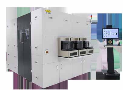
EV Group Solutions for Compound Semiconductor Manufacturing
|
|
|
- Ruby Burke
- 6 years ago
- Views:
Transcription

1 EV Group Solutions for Compound Semiconductor Manufacturing

2 EV Group Solutions for Compound Semiconductor Manufacturing Introduction Compound semiconductor devices have been linked with airborne and military applications for a long time. More recently, with increasing requirements from consumer electronics, compound semiconductors found inroads to large-scale production. In particular, rising data volumes and transmission speeds for mobile devices enabled high growth rates of radio front-end devices, consisting of three basic building blocks, namely filter/duplexer, power amplifier and antenna switch. All of these parts are being manufactured to a large extent of compound semiconductors. Besides radio front-end application on GaAs substrates novel applications arise, increasing the importance of compound semiconductors for several applications. As an example, photonic interconnects for high speed, low State-of-the-art Die-Sized SAW package (DSSP ) Copyright EPCOS AG 2013 loss and largely improved bandwidth is one of them. These devices are mostly indium phosphide (InP) based. Since InP is difficult to grow on low cost wafers and with large size, wafer bonding considerably gains importance. In general, wafer bonding and more specifically direct wafer bonding with the aid of plasma activation, levels the ground for compound semiconductors to be implemented in a complementary metal oxide semiconductor (CMOS) production scale. With the maturing market position of compound semiconductors, common processing and packaging technologies from advanced CMOS and micro electro mechanical systems (MEMS) are paving its way. Advanced packaging is one prominent example, where CMOS and compound semiconductor design and processing blend together. EV Group is a recognized leader of processing technology for wafer bonding, optical lithography, nanoimprint lithography and wafer level packaging. EVG's Process Portfolio...etc. EVG Processes Wafer & Template Fabrication Substrate Bonding for SOI Substrate Cleaning Plasma Activation Resist Coating Spin/Spray Alignment Verification Proximity Lithography Nanoimprint Lithography Resist Developing Metallization RIE, DRIE Wet Etching Resist Lift-Off CVD, LPCVD, PVD,... Thermal Oxide Growing Bond Alignment Thinning, CMP Wafer Bonding Temporary Bonding/ Debonding Wafer Dicing Stress Relief Etching Electroplating Chip-to- Wafer Bonding Wafer Bumping & Redistribution 2

 or for selective area growth of nanowires.")

 is an ideally suited replication method for such nanometer")


 Working stamp can be used multiple times before disposal Imprint nanostructures UV curing")
3 Nano Imprint Lithography Nano patterns are a novel topic for most parts of the compound semiconductor applications. Recently, nano patterns spurred a lot of attention for growth substrates, such as nano patterned sapphire substrates (npss) or for selective area growth of nanowires. However, these are not the only solutions. Photonic elements, such as wire grid polarizers, color filters or gratings, are frequently used applications, facilitating nano patterns in compound semiconductors. Nano imprint lithography (NIL) is an ideally suited replication method for such nanometer structures. The typical properties of compound semiconductor substrates high bow, varying TTV and defects after epitaxial growth have been shown to be challenging for conventional lithography methods. Same is true for high resolution capability of less than 50 nm, which is needed for many photonic applications. EVG s lineup of NIL tools fulfills all above requirements, in order to provide a cost effective, high quality, full-field nano patterning. Advantages of EVG s nano imprint lithography solution: Same tool for imprinting and stamp replication Mask lifetime comparable to lithography masks Room-temperature process without run-out or alignment issues due to thermal expansion in stamp manufacturing and imprinting Control of stamp material (Young s modulus, surface energy...) Working stamp can be used multiple times before disposal Imprint nanostructures UV curing Detach Stamp Reuse stamp Dispense liquid resin Parallel alignment of stamp and substrate Imprint at low pressure Expose with UV light through stamp and crosslink Photonic structures on the top surface greatly enhance the LED light output Detach stamp from substrate Reuse soft stamp SEM image of a photonic crystal fabricated by nanoimprint lithography 3 Micro contact printing tool in the EVG 620 EVG 7200 Automated UV-NIL System up to 200 mm EVG SmartNIL full area imprinted 150 mm Si substrate 3


4 EV Group Solutions for Compound Semiconductor Manufacturing Wafer Bonding for Compound Semiconductors Direct wafer bonding for heterogeneous integration of compound semiconductors Several applications as power, RF, biosensing, photovoltaic and photonic devices will benefit from improvements in power efficiency, performance, size, weight, reliability and cost driven by the integration of compound semiconductor materials. These improvements are often referred to as More than Moore, since they are not directly related to lithographic scaling, and they are enabling an ever increasing array of electronic devices and applications. Today s plasma-activated direct bonding processes give additional freedom for the device design and process implementation. It has been proven for several years that most compound semiconductors can be directly bonded on different substrates. This was enabled by plasma-activated fusion bonding, which lowers the required anneal temperatures below critical temperature levels that can cause wafers to break because of the stress induced by differences in the thermal expansion coefficients. This method incorporates a SiO 2 bond interface, which can be as thin as the native oxide. Some devices can benefit from this oxide layer as it reduces parasitic effects like leakage current or cross talk to the substrate. Advantages of fusion bonding for compound semiconductors: Direct stacking of heterogenous compound semiconductors Use of inexpensive carrier substrates for processing and re-use of expensive epitaxial growth wafers Generation of advanced, complex and novel devices stacks by direct wafer bonding Recent technology developments such as EVG s ComBond technology, can provide a covalent oxide-free bond interface. Furthermore, this new approach enables the joining of different materials at very low or room temperature, which keeps the thermally induced stress between the wafers to a minimum. EVG 580 ComBond Automated High-Vacuum wafer Bonding System - Enabling oxide free electrically conductive interfaces The EVG580 ComBond adds a new milestone to EVG s unique portfolio of wafer bonding equipment and technology in response to market needs for more sophisticated integration processes to combine materials with different lattice constant and coefficient of thermal expansion (CTE). Wafer bonding can combine different substrate materials while avoiding defects due to lattice and CTE mismatch that are associated with traditional epitaxial processes. Room-temperature covalent bonding, in particular, is an ideal choice since it eliminates the need for annealing processes, which generate high temperatures that can add additional stress due to CTE mismatch. However, a key limitation of room-temperature covalent bonding has been the inability to maintain tight control of the thickness and uniformity of the bond interface, including effective removal of particle contaminants and the native oxide layers. These are necessary in order to achieve an interface that has both sufficient bond strength and electrical conductivity between the bonded materials. The EVG580 ComBond wafer bonding platform combines several technology breakthroughs to enable the formation of bond interfaces between heterogeneous materials at room temperature while achieving excellent bond strength and electrical conductivity. GaAs 200mm LowTemp plasma activation chamber EVG 580 ComBond Automated High-Vacuum Wafer Bonding System 2 nm InP GaAs InP Bond Interface* *Courtesy of Fraunhofer ISE 4


5 Wafer Level Die Bonding The wafer level die transfer bonding concept separates the two processes of chip placement on the wafer and the actual chip-to-wafer bonding process. Nonetheless, a wafer level approach still has several key advantages, such as collective pre-processing of the dies and high bonding throughput. This cannot be provided easily with die-to-die bonding. However, a wafer-level die transfer process combines the best of both worlds, which is the fast distribution of the known good die (KGD) and high-quality direct bonding at the wafer level. Furthermore, this easily allows tuning of bonding conditions as it enables collective bonding at elevated temperatures or even in vacuum conditions. A key requirement to enable such a process is to apply uniform pressure on every single die, not just generally over the whole wafer. As shown in the figure on the right hand side, several issues can occur that inhibit a homogenous pressure distribution. Thus, the process has to be set up to comply with bow and warpage, unevenness of the substrate as well as die height variations. Introducing a compliant layer can compensate for these challenges and enable the application of similar force on the different die, thus providing optimal transfer rates and high bonding yield. In this way, heterogeneous integration can be scaled up to larger substrates and multiple functions can be added to the device wafer even in volume production. Multi-Substrate Bonding EV Group has implemented multi-substrate bonding in combination with a high system throughput. The unique design of EVG s multi-substrate wafer bonders maintain high system flexibility to bond different substrate sizes on the same equipment with minimal changeover time. Field proven compliant layer technology avoids chipping and breakage of valuable wafers. EVG s fully automated wafer bonding system for LED manufacturing offers flexible tool support for metal, adhesive and fusion bonds of various substrate types. Cassette-to-cassette operation, multisubstrate bonding capability and a modular design with up to four swap-in process modules make the EVG500 series the perfect solution for LED manufacturing from R&D to HVM needs. EVG s field proven wafer bonding technology, as well as the unique approach to low temperature metal wafer bonding, results in high throughput and yields. Multi-substrate bonding systems for LEDs High throughput up to 160 bonds/h (50 mm wafer equivalents) Optimized pressure and temperature uniformity for highest possible yield Automatic handling of bowed and warped wafers Low temperature metal wafer bonding Integrated pre-processing modules for low-temperature metal wafer bonding Eutectic, Transient-Liquid-Phase (TLP) and thermo-compression bonding E.g. Au-Au, Au-In, Au-Sn, Cu-Sn, Cu-Cu,... Cross section SEM image of Au:Sn bonded wafers C-SAM image of a patterned wafer pair bonded with Au:Sn EVG 500 Series Bond Module Fully Automated Wafer Bonding System for High-Volume Manufacturing 5


, especially important for expensive encapsulates such as PBO, BCB or polyimide Universal")
 Spray")

6 EV Group Solutions for Compound Semiconductor Manufacturing Back End Wafer Processing EVG OmniSpray for polymeric and photoresist coatings Polymer coatings enable improved functionality for compound semiconductor devices. Besides their use as insulating layers, polymer coatings exhibit advantages for other applications. The low dielectric constant (low-k) of polymers facilitated higher switching frequencies of compound semiconductor devices. In turn, this enables faster data standards. On the other hand, elevated on-chip interconnects called air bridges, are used for the same reason. To cope with reliability demands, these fragile gold structures need rigid support. In addition, polymers such as PBO or BCB are standard for scratch protection layers, as an overcoat to protect the wafer front side for the following back side processing. EVG s OmniSpray technology is a universal coating technology that accomplishes such demanding coating applications. Depending on the application, different types of polymer compounds are available on the market, such as epoxies, polyimides, BCB, PBO or silicones. Varying material characteristics, hence varying process requirements, recommend OmniSpray as universal coating technology. In addition, OmniSpray helps to reduce material usage up to 80%, considerably lowering the bill of material and working on an improved cost-of-ownership. Advantages of EVG s OmniSpray for Compound semiconductors: Reduced resist consumption (up to 80%), especially important for expensive encapsulates such as PBO, BCB or polyimide Universal technology to coat polymers with largely varying solids content and viscosities Ideal for planarization applications (spray / spin process combination) Uniform coating of deep trenches and high aspect ratio features Special setup for high viscosity polymers Ideal for thick resist coating applications Underfill Process with spray and spin coating (courtesy of Agilent Technologies) Spray coated cavities with high topography EVG proprietary OmniSpray resist atomization nozzle EVG 150 Fully-automated Resist Processing System: Coating of thick and thin resists such as required for optical lithography and adhesive packaging Spin and spray coating capability in the same bowl Spray Coating with X-Y Scanning or rotary motion Simplified operator usability and serviceability Reduced process qualification time Minimized footprint for highest fab utilization Fast changeover times for multiple substrate sizes Advanced handling and processing of bowed / warped wafers EVG 150 Fully-automated Resist Processing System up to 200mm EVG 150 Modular tool layout for highest flexibility EVG 150 Modular chemical storage units and advance tool access for optimized serviceabiliy 6

, are just a few of the most common applications.")


 High print resolution for homogenous current distribution Advanced handling and processing of bowed / warped")
7 Back End Wafer Processing Optical Lithography Optical lithography is still a work horse for multiple applications in compound semiconductor manufacturing. Device structures on the semiconductor wafer, encapsulation based wafer level packaging, bumping, patterning of through wafer vias (TWV), are just a few of the most common applications. Compound semiconductor specific requirements: Processing of bowed/warped as well as transparent substrates Image recognition of shallow etching-generated topography: Development of special optics to align such low-contrast structures is a key for highest overlay accuracy and maximum process yield. Customized wafer chuck designs for efficient flattening of compound semiconductor wafers and hence a constant print gap Non-contact processing of delicate and brittle compound semiconductor wafer for maximum yield Processing of thin wafers: Thin wafers with sufficient thickness to be self-supportive, can be directly being processed with special handling and process options. If this is not the case, thin wafers are typically carrier mounted and the thin wafers are processed on top. Both EVG aligner platforms the EVG620/EVG6200 series as well as the IQ Aligner are designed for compound semiconductor characteristic processing specifications. EVG 620 HBL Fully-automated mask aligner for compound semiconductors: Attractive Cost-of-Ownership and low CapEx High throughput (165 wafers/h in aligned mode / 220 wafers/h for first print applications) High overlay accuracy for multiple mask processing (front-to-front side, front-to-back side) High print resolution for homogenous current distribution Advanced handling and processing of bowed / warped wafers Fast changeover times for multiple substrate sizes Image based pre-aligner for transparent or sapphire mounted wafers Thin wafer and carrier mounted wafer processing EVG 620 HBL Fully-automated mask aligner for compound semiconductor manufacturing EVG 620 Mask Alignment System: easy access for manual loading for wafers and also wafer pieces EVG 620 Handling module with 5 cassette stations allows processing of 125 wafers per process run EVG 620NT Manual Mask/ Bond Alignment System 7


8 EV Group Solutions for Compound Semiconductor Manufacturing Back Side Wafer Processing Temporary Bonding and Debonding for advanced thin wafer handling Compound semiconductor materials such as GaAs, SiC, LiTaO 3 or InP offer distinct electrical advantages, but typically suffer from the low thermal conductivity. The most effective method for heat transfer is wafer thinning. Due to the brittleness of these materials, thin compound semiconductor wafers are temporarily bonded to a rigid carrier for thinning and back side processing. The bonded wafers can be processed in standard fabs with standard equipment. Thermal management of compound semiconductor devices was the primary driver for thin wafers and devices in the past. Recently, the reduced form factor has become the most important driver. The starting point is a device wafer with complete front-end processing on the front side of the wafer. This device wafer is bonded to a carrier wafer with its front side in the bond interface. After bonding the first step is back-thinning of the wafer. Usually back-thinning is a multistep process consisting of mechanical back-grinding and subsequent stress relief etching and polishing. After back-thinning the back side of the device wafer can be processed using standard wafer fab equipment. The carrier wafer gives mechanical support and stability and protects the fragile wafer edge of the thin wafer. Finally, when all back side processing is done, the wafer gets debonded, cleaned and transferred to a film frame or to other output formats. EV Group provides production equipment for temporary bonding and debonding since We have the largest install base and are the clear market share leader. EV Group has more than 20 years of experience in wafer bonding. Temporary Bonding / Debonding Principle Temporary Bonding Debonding Device Wafer Front-End Processing (Lithography, etching, etc.) Wafer Stack mounted on Film Frame Device Wafer Debonding Carrier Wafer with Adhesive Film Temporary Bonding Device Wafer bonded on Carrier Wafer Cleaning Back Thinning and further Processing Device Wafer (thinned) on Carrier Wafer Thin Wafer on Film Frame Double end effectors for rapid wafer handling EVG 820 Adhesive Tape Punch Module Thin 6" wafer mounted onto dicing tape 8


9 LowTEMP Debonding EVG ZoneBond Open Platform EVG LowTemp ZoneBOND is a revolutionary breakthrough in thin-wafer processing. It enables room temperature debonding, which is independent of the properties of the temporary adhesive, providing a versatile supply chain with multiple adhesive suppliers. EVG ZoneBond Debonding Technology Features: EVG ZoneBond Open Platform, including license for ZoneBond with multiple adhesives Breaking the link between the debonding method and adhesive properties Fully automated carrier preparation integrated into the high volume manufacturing EVG850TB/DB system Multilayer Adhesive Debonding EVG LowTemp debonding technology includes room temperature multilayer adhesive debonding, where the separation of the carrier and device wafer is initiated mechanically. Several temporary bonding adhesives are available for this debonding solution. EVG Multilayer Adhesive Debonding: Room temperature debonding by mechanical separation Universal equipment technology enabling all common mechanical debond adhesives and techniques Full control and monitoring of the mechanical debonding process Laser-Initiated Debonding The laser debonding process being developed at EVG is based on excimer lasers. For their spectral range, standard glass carriers offer high transmission, keeping carrier cost low. In contrast to laser induced thermal debonding, the ultraviolet light emitted by excimer lasers is absorbed within a few hundred nanometers of the glass/adhesive interface, thereby leaving the thin wafer entirely unaffected. EVG Laser Debonding Technology Features: No thermal stress subjected to the device wafer Lowest cumulative costs in virtue of single adhesive layer technology requiring no additional release layer application High throughput capability using field proven excimer laser technology High thermal resistance up to 350 C Thermal Debonding Thermal Slide-Off Debonding Thermoplastic adhesives are rigid at room temperature, but have reduced viscosity at elevated temperature. This drop in viscosity enables a unique debonding mechanism - thermal slide-off debonding. At the debonding temperature, the viscosity of the adhesive is reduced, which enables a controlled debonding of the thin device wafer from the carrier wafer. Slide-Off Debonding Technology Features: High volume, production proven technology Industry leading thin wafer handling and cleaning technology for highest yield without wafer breakage Market leading solutions in thermal sliding and thin wafer handling Thermal Lift-Off Debonding Multiple dry film adhesive tapes are available for temporary bonding. Dry film adhesive tapes usually consist of a backing foil with adhesive films plus protective liners on both sides. Both adhesive films are bondable, but different debonding mechanisms are used for either side. This allows controlled debonding, whereby the separation between thin device wafer and carrier wafer happens at the interface between device wafer and tape. Next, the tape is peeled off of the carrier wafer, which enables recycling of the carriers. EVG 850TB Spin Coat Module EVG 850DB Debond Module EVG 850DB Film Frame Mount Module 9
 is a mainstream technology in micro electro mechanical systems (MEMS) and advanced")


10 EV Group Solutions for Compound Semiconductor Manufacturing Wafer Level Packaging Introduction to Wafer Level Packaging (WLP) Today, wafer level packaging (WLP) is a mainstream technology in micro electro mechanical systems (MEMS) and advanced complementary metal oxide semiconductor (CMOS). Bringing this packaging technology to compound semiconductors enables more compact packages, imperative for consumer devices. The wafer-level approach furthermore helps for cost reduction and ramping to high production volumes. Major benefits for wafer level packaging of compound semiconductors are: Batch fabrication packaging processes Compact packaging possible Increased functional density Improved circuit performance Reduce higher order assembly cost, relax module assembly requirement Hermetic packaging possible These days, WLP is grouped into an cap-based and encapsulation-based packaging approach. Encapsulation-based Wafer Level Packages Encapsulation-based wafer level packaging (WLP) is besides capping-based WLP most prominent in the market right now. Major difference to prior discussed packages formed by wafer bonding is the creation of a protecting shell by thin film deposition. Depending on the requirements of the later package, either inorganic shell materials, for vacuum and hermetic packages, or polymer materials are used. For polymers, shielding is not gas-tight. However, for consumer electronics protection from environmental influences, moisture and dirt, gives sufficient durability. 1. Spin on UV curable resist 4. UV exposure of resist 2. UV exposure of resist 5. Development of resist 3. Vertical sidewalls within the resist 6. Sealing of the package in controlled atmosphere EVG s resist processing & mask aligner technology for encapsulation-based WLP features: Coating and patterning of sacrificial spacers, defining the cavity dimension and volume Etching mask generation for openings in inorganic films such as oxide or nitride based capping layers Direct patterning of photoactive polymer encapsulates, such as SU8, BCB or ShinEtsu SINR Wet chemical sacrificial layer removal of over coating and enclosure device cavities Etch mask patterning or lithographic opening of electrical contacts EVG GEMINI Fully Automated Wafer Bonding System EVG 500 Series Bond Module SmartView Align Module 10


11 Wafer Level Packaging Capping-based Wafer Level Packaging Wafer-level capping is already a common process for MEMS and CMOS packaging. However, standard processes from these markets are most of the time not directly applicable to compound semiconductor packaging. A generic manufacturing process is depicted below. Depending on the sealing material, the according bonding temperature is directly influenced, same as the sealing characteristics. Requirements for wafer bonding of compound semiconductor WLP are stringent. Deep know-how of various bonding techniques and decision factors for each of them is one of EVG s strengths. In the case of capping-based WLP, where interlayers in the form of sealing rings are patterned prior to bonding, the following techniques and materials are most prominent in the market right now: Eutectic Bonding Solder Bonding Thermally cured adhesive bonding EVG s extensive experience of more than 25 years in the wafer bonding market guarantees for best bonding results and highest yields. EVG s core competences comprise wafer to wafer alignment, temperature distortion management for lowest bow, strain engineering, leading planarity, bonding of brittle substrates, and many more. Direct Bonding Molecular Bonding Anodic Bonding Wafer Bonding Eutectic Bonding Metal Bonding Solder Bonding Bonding with Inter-Layers Glass Frit Bonding Adhesive Bonding Metal Thermocompression Bonding UV-Cured Polymer Thermally Cured Polymer Schematic wafer level capping process flow Flow chart covering all wafer bonding technologies featured on EVG bonders with prominent CS WLP techniques highlighted in red Source: EVG KMPR cavity sidewall produced on a EVG 150 and EVG 620 (Source: Triquint, presented at CSMantech 2012) EVG Logo in 400µm SU-8 on 6" Wafer IQ Aligner Topside mask alignment 11


 Debonding Wafer")
12 EV Group Solutions for Compound Semiconductor Manufacturing Nano Imprint Lithography Solutions EVG 620NT Semi-Automated UV-NIL, µ-cp System up to 150 mm UV Nano Imprinting Microcontact Printing EVG 720/7200 Automated UV-NIL System up to 150/200 mm UV Nano Imprinting EVG SmartNIL TM EVG 770 Automated NIL Stepper up to 300 mm UV Nano Imprinting Step-and-Repeat Imprinting Master Fabrication Cleaning and Metrology EVG 301 Semi-automated Single Wafer Cleaning System to 300 mm Megasonic Cleaning Brush cleaning DI-water / Diluted Chemicals EVG 40NT Semi-automated Measurement System up to 300 mm Overlay Alignment Verification Front-to-Backside Alignment Verification EVG 40NT Automated Measurement System up to 300 mm Overlay Alignment Verification Front-to-Backside Alignment Verification Advanced Wafer Handling Temporary Bonding Solutions EVG 805 Semi-automated Debonding System up to 300 mm EVG 820 Lamination System up to 300 mm EVG 850TB Automated Temporary Bonding System up to 300 mm EVG 850DB Automated Debonding System up to 300 mm Debonding Advanced Wafer Handling Integrated Dry Film Lamination from Temporary Bonding 50 mm mm Coat, Bake and Bond Precision Aligned Lamination on Modules Carrier Wafer Protective Film Remover (de-lamination) Debonding Wafer Cleaning Film Frame Mounting 12


 Lithography Solutions")


13 Resist Processing Solutions EVG 101 Advanced Resist Processing System up to 300 mm Spin Coating Spray Coating EVG 120 Automated Resist Processing System up to 300 mm Spin Coating Spray Coating Bake Advanced Wafer Handling EVG 150 Automated Resist Processing System up to 300 mm Spin Coating Spray Coating Bake Advanced Wafer Handling Lithography Solutions EVG 620NT Automated Mask Alignment System up to 150 mm Mask Alignment Bond Alignment Advanced Wafer Handling EVG 620 HBL Automated Mask Alignment System up to 150 mm Mask Alignment Bond Alignment Advanced Wafer Handling IQ Aligner Automated Mask Alignment System up to 300 mm Mask Alignment Bond Alignment Advanced Wafer Handling Integrated (Nanoimprint) Lithography Solutions HERCULES L Lithography Track System resist processing & expose configuration up to 300 mm Spin Coating Spray Coating Bake Mask Alignment Advanced Wafer Handling HERCULES Lithography Track System coat/align & expose/develop configuration up to 300 mm Spin Coating Spray Coating Bake Mask Alignment Advanced Wafer Handling Developing HERCULES NIL Integrated UV-NIL Track System up to 200 mm Cleaning Spin Coating Bake SmartNIL TM Nanoimprinting 13


14 EV Group Solutions for Compound Semiconductor Manufacturing Bond Alignment Solutions EVG 620 Semi-Automated Bond Alignment System up to 150 mm EVG 6200 Semi-Automated Bond Alignment System up to 200 mm SmartView NT Automated Bond Alignment System for Universal Alignment up to 300 mm Bond Alignment Bond Alignment Bond Alignment Wafer Bonding / Hot Embossing Solutions EVG 510HE Semi-automated Hot Embossing System up to 200 mm Hot Embossing High-Temperature Embossing EVG 520IS Semi-automated Wafer Bonding System up to 200 mm Permanent Bonding Multi-Substrate Bonding EVG 540 Automated Wafer Bonding System up to 300 mm Permanent Bonding Multi-Substrate Bonding Integrated Wafer Bonding Solutions EVG 560 Automated Wafer Bonding System up to 300 mm Mechanical Alignment Permanent Bonding Multi-substrate Bonding GEMINI Automated Production Wafer Bonding System up to 300 mm Optical Alignment Permanent Bonding Multi-substrate Bonding Plasma Activation Wafer Cleaning EVG 580 ComBond Automated High-Vacuum Wafer Bonding System up to 200 mm Covalent, Oxide-free Bonding Room Temperature Bonding High-Vacuum Bonding Optical Prealigner 14
15 Overview: EVG s Process Capabilities Cleaning Spin Coating Spray Coating Nano Spray Bake Mask Alignment UV Nano Imprinting Alignment Verification Developing Bond Alignment Wafer Bonding Plasma Activation Lens Molding Edge handling for double-side cleaning; Megasonic nozzles or area transducers; Scrubber brush; Compatible with solvents, removers and diluted chemicals Thin and thick resist processing; Programmable dispense arm for various dispense modes High topography coating; Deep etched cavities; Coating of square, irregular shaped and perforated substrates Through silicon via coating; Sidewall passivation High temperature uniformity; Proximity heating; Edge handling Optical pattern recognition of low contrast samples; Topside alignment; Bottomside alignment; Transmissive and reflective IR; Shadow mask alignment Full-field nano imprinting; Step and repeat master replication Overlay measurement; Top to bottom measurement Spray, stream and puddle dispensing; Fully programmable dispenser Through wafer alignment; Backside alignment; Transmissive and reflective IR; SmartView alignment Thermocompression bonding; Eutectic bonding; Transient liquid phase bonding; Fusion bonding; Anodic bonding; Adhesive bonding; Glass frit bonding Plasma activation for semiconductor direct bonding Wafer level optics for beam shaping; Step and repeat lens master fabrication; Temporary Bonding / Debonding Advanced Wafer Handling Processing of thin wafers, bow, warped or fragile substrates; Various bonding and debonding processes Handling of thin, warped or fragile wafers; Edge wafer handling; Special endeffectors 15
16 EV Global Group Locations Solutions for Compound Semiconductor Manufacturing Headquarters Worldwide Sales and Customer Support EV Group Europe & Asia/Pacific GmbH DI Erich Thallner Strasse St.Florian am Inn Austria Phone: Fax: Sales@EVGroup.com Germany EV Group E. Thallner GmbH Hartham Neuhaus Germany Phone: Fax: Sales@EVGroup.com Europe Tech Support Phone: TechSupportEU@EVGroup.com Japan EV Group Japan KK Yokohama Business Park East Tower 1F 134, Godo-cho, Hodogaya-ku, Yokohama-shi, Kanagawa, Phone: Fax: Sales@EVGroup.jp Japan Tech Support Phone: (Yokohama) Phone: (Fukuoka) TechSupportJP@EVGroup.com Korea EV Group Korea Ltd. Room 503, Seokun Tower, 178, Pangyoyeok-ro, Bundang-gu, Seongnam-si, Gyeonggi-do, , South Korea Phone: Fax: Sales@EVGroup.co.kr North America EV Group Inc South River Parkway Tempe, AZ Phone: Fax: SalesUS@EVGroup.com EV Group Inc. 100 Great Oaks Blvd; Suite #119 Albany, NY SalesUS@EVGroup.com North America Tech Support Phone: TechSupportUS@EVGroup.com Taiwan Sales EVG-JOINTECH CORP. No. 400, Hwang-Pei Road Chung-Li City, Phone: Fax: Sales@EVG-Jointech.com.tw Taiwan Customer Support EV Group Taiwan Ltd. North Office: No. 400, Hwang-Pei Road Chung-Li City, South Office: Rm203, NO.12, Nanke 2nd RD, Xinshi Dist., Tainan City, Phone: Fax: (North Office) Fax: (South Office) CustomerSupportTW@EVGroup.com China EV Group China Ltd. Room , Building No. 3, No. 498 Guo Shou Jing Road, Zhangjiang High-Tech Park, Pudong New Area, Shanghai, PR China, Shanghai Phone: Fax: Sales@EVGroup.cn ServiceCN@EVGroup.com Data, design and specifications may not simultaneously apply; or depend on individual equipment configuration, process conditions and materials and may vary accordingly. EVG reserves the right to change data, design and specifications without prior notice. All trademarks, logos, website addresses or equipment names that contain the letters or words EVG or EV Group or any combination thereof, as well as the following names and acronyms are registered trademarks and/or the property of EV Group: ComBond, CoverSpin, EZB, EZ Bond, EZD, EZ Debond, EZR, EZ Release, GEMINI, HERCULES, HyperIntegration, IQ Aligner, LowTemp, NanoAlign, NanoFill, NanoSpray, NIL-COM, NILPhotonics, OmniSpray, SmartEdge, SmartNIL, SmartView, The Triple i Company Invent-Innovate-Implement, Triple i. Other product and company names may be registered trademarks of their respective owners. ZoneBOND is a registered trademark of Brewer Science, Inc. Other product and company names may be registered trademarks of their respective owners. Printed on paper from sustainable sources EV Group (EVG). All rights reserved. V01/16 16
EVG 810LT Series LowTemp Plasma Activation Systems
 EVG 810LT Series LowTemp Plasma Activation Systems EVG 810LT Series LowTemp Plasma Activation Systems Introduction EV Group s LowTemp (LT) Plasma Activated Bonding is available for both R&D and high volume
XBC300 Gen2. Fully-automated debonder and Cleaner
 XBC300 Gen2 Fully-automated debonder and Cleaner XBC300 Gen2 FULLY AUTOMATED DEBONDER AND CLEANER The SUSS XBC300 Gen2 debonder and cleaner platform is designed for process development as well as high
1
 Process methodologies for temporary thin wafer handling solutions By Justin Furse, Technology Strategist, Brewer Science, Inc. Use of temporary bonding/debonding as part of thin wafer handling processes
EV Group. Enabling processes for 3D interposer. Dr. Thorsten Matthias EV Group
 EV Group Enabling processes for 3D interposer Dr. Thorsten Matthias EV Group EV Group in a Nutshell st Our philosophy Our mission in serving next generation application in semiconductor technology Equipment
Update in Material and Process Technologies for 2.5/3D IC Dr. Rainer Knippelmeyer CTO and VP R&D, SÜSS MicroTec AG
 Update in Material and Process Technologies for 2.5/3D IC Dr. Rainer Knippelmeyer CTO and VP R&D, SÜSS MicroTec AG TEMPORARY BONDING / DEBONDING AS THIN WAFER HANDLING SOLUTION FOR 3DIC & INTERPOSERS Device
EV Group. Engineered Substrates for future compound semiconductor devices
 EV Group Engineered Substrates for future compound semiconductor devices Engineered Substrates HB-LED: Engineered growth substrates GaN / GaP layer transfer Mobility enhancement solutions: III-Vs to silicon
Thin Wafer Handling Challenges and Emerging Solutions
 1 Thin Wafer Handling Challenges and Emerging Solutions Dr. Shari Farrens, Mr. Pete Bisson, Mr. Sumant Sood and Mr. James Hermanowski SUSS MicroTec, 228 Suss Drive, Waterbury Center, VT 05655, USA 2 Thin
SHRINK. STACK. INTEGRATE.
 SHRINK. STACK. INTEGRATE. SUSS MICROTEC PRODUCT PORTFOLIO SHAPING THE FUTURE With more than 60 years of engineering experience SUSS MicroTec is a leading supplier of process equipment for microstructuring
LATEST INSIGHTS IN MATERIAL AND PROCESS TECHNOLOGIES FOR INTERPOSER AND 3D STACKING
 LATEST INSIGHTS IN MATERIAL AND PROCESS TECHNOLOGIES FOR INTERPOSER AND 3D STACKING European 3D TSV Summit, January 22-23, 2013, Grenoble Dr. Rainer Knippelmeyer, CTO and VP of R&D, GM Product Line Bonder
Temporary Wafer Bonding - Key Technology for 3D-MEMS Integration
 Temporary Wafer Bonding - Key Technology for 3D-MEMS Integration 2016-06-15, Chemnitz Chemnitz University of Technology Basic Research Fraunhofer ENAS System-Packaging (SP) Back-End of Line (BEOL) Applied
Passionately Innovating With Customers To Create A Connected World
 Passionately Innovating With Customers To Create A Connected World Multi Die Integration Can Material Suppliers Meet the Challenge? Nov 14, 2012 Jeff Calvert - R&D Director, Advanced Packaging Technologies
CURRENT STATUS OF NANOIMPRINT LITHOGRAPHY DEVELOPMENT IN CNMM
 U.S. -KOREA Forums on Nanotechnology 1 CURRENT STATUS OF NANOIMPRINT LITHOGRAPHY DEVELOPMENT IN CNMM February 17 th 2005 Eung-Sug Lee,Jun-Ho Jeong Korea Institute of Machinery & Materials U.S. -KOREA Forums
A Temporary Bonding and Debonding Technology for TSV Fabrication
 A Temporary Bonding and Debonding Technology for TSV Fabrication Taku Kawauchi, Masatoshi Shiraishi, Satoshi Okawa, Masahiro Yamamoto Tokyo Electron Ltd, Japan Taku Kawauchi, Tokyo Electron Ltd./Slide
Structuring and bonding of glass-wafers. Dr. Anke Sanz-Velasco
 Structuring and bonding of glass-wafers Dr. Anke Sanz-Velasco Outline IMT Why glass? Components for life science Good bond requirements and evaluation Wafer bonding 1. Fusion bonding 2. UV-adhesive bonding
Hybrid Wafer Level Bonding for 3D IC
 Hybrid Wafer Level Bonding for 3D IC An Equipment Perspective Markus Wimplinger, Corporate Technology Development & IP Director History & Roadmap - BSI CIS Devices???? 2013 2 nd Generation 3D BSI CIS with
EE C245 ME C218 Introduction to MEMS Design Fall 2007
 EE C245 ME C218 Introduction to MEMS Design Fall 2007 Prof. Clark T.-C. Nguyen Dept. of Electrical Engineering & Computer Sciences University of California at Berkeley Berkeley, CA 94720 Lecture 12: Mechanics
Regents of the University of California
 Deep Reactive-Ion Etching (DRIE) DRIE Issues: Etch Rate Variance The Bosch process: Inductively-coupled plasma Etch Rate: 1.5-4 μm/min Two main cycles in the etch: Etch cycle (5-15 s): SF 6 (SF x+ ) etches
Page Films. we support your innovation
 Page Films we support your innovation Page Films SAES Thin Film Technology: the Evolution of the Getter Integration Pioneering the development of getter technology, the SAES Getters Group is the world
Self-study problems and questions Processing and Device Technology, FFF110/FYSD13
 Self-study problems and questions Processing and Device Technology, FFF110/FYSD13 Version 2016_01 In addition to the problems discussed at the seminars and at the lectures, you can use this set of problems
F R A U N H O F E R I N
 FRAUNHOFER Institute FoR Electronic NAno systems ENAS System Packaging 1 2 3 4 5 The actual developments of micro and nano technologies are fascinating. Undoubted they are playing a key role in today s
Thin Wafer Handling Debonding Mechanisms
 Thin Wafer Handling Debonding Mechanisms Jonathan Jeauneau, Applications Manager Alvin Lee, Technology Strategist Dongshun Bai, Scientist, 3-D IC R&D Materials Outline Requirements of Thin Wafer Handling
Lecture 14 Advanced Photolithography
 Lecture 14 Advanced Photolithography Chapter 14 Wolf and Tauber 1/74 Announcements Term Paper: You are expected to produce a 4-5 page term paper on a selected topic (from a list). Term paper contributes
Avatrel Dielectric Polymers for Electronic Packaging
 Avatrel Dielectric Polymers for Electronic Packaging R. A., Shick, S. K. Jayaraman, B. L. Goodall, L. F. Rhodes, W.C. McDougall Advanced Technology Group BF Goodrich Company 9921 Brecksville Road Cleveland,
Techniken der Oberflächenphysik (Techniques of Surface Physics)
") Techniken der Oberflächenphysik (Techniques of Surface Physics) Prof. Yong Lei & Dr. Yang Xu (& Liying Liang) Fachgebiet 3D-Nanostrukturierung, Institut für Physik Contact: yong.lei@tu-ilmenau.de; yang.xu@tu-ilmenau.de;
Techniken der Oberflächenphysik (Techniques of Surface Physics) Prof. Yong Lei & Dr. Yang Xu (& Liying Liang) Fachgebiet 3D-Nanostrukturierung, Institut für Physik Contact: yong.lei@tu-ilmenau.de; yang.xu@tu-ilmenau.de;
Chapter 3 : ULSI Manufacturing Technology - (c) Photolithography
 Photolithography") Chapter 3 : ULSI Manufacturing Technology - (c) Photolithography 1 Reference 1. Semiconductor Manufacturing Technology : Michael Quirk and Julian Serda (2001) 2. - (2004) 3. Semiconductor Physics and Devices-
Chapter 3 : ULSI Manufacturing Technology - (c) Photolithography 1 Reference 1. Semiconductor Manufacturing Technology : Michael Quirk and Julian Serda (2001) 2. - (2004) 3. Semiconductor Physics and Devices-
HSG-IMIT Application AG
 B4.1 Acceleration Sensors IP-Blocks for MEMS Foundry Surface Micromachining Process R. Knechtel, S. Dempwolf S. Hering X-FAB Semiconductor Foundries AG Haarberstraße 67 99097 Erfurt / Germany T. Link J.
Three Approaches for Nanopatterning
 Three Approaches for Nanopatterning Lithography allows the design of arbitrary pattern geometry but maybe high cost and low throughput Self-Assembly offers high throughput and low cost but limited selections
Wet Chemical Processing with Megasonics Assist for the Removal of Bumping Process Photomasks
 Wet Chemical Processing with Megasonics Assist for the Removal of Bumping Process Photomasks Hongseong Sohn and John Tracy Akrion Systems 6330 Hedgewood Drive, Suite 150 Allentown, PA 18106, USA Abstract
Technologies VII. Alternative Lithographic PROCEEDINGS OF SPIE. Douglas J. Resnick Christopher Bencher. Sponsored by. Cosponsored by.
 PROCEEDINGS OF SPIE Alternative Lithographic Technologies VII Douglas J. Resnick Christopher Bencher Editors 23-26 February 2015 San Jose, California, United States Sponsored by SPIE Cosponsored by DNS
ALIGNMENT ACCURACY IN A MA/BA8 GEN3 USING SUBSTRATE CONFORMAL IMPRINT LITHOGRAPHY (SCIL)
") ALIGNMENT ACCURACY IN A MA/BA8 GEN3 USING SUBSTRATE CONFORMAL IMPRINT LITHOGRAPHY (SCIL) Robert Fader Fraunhofer Institute for Integrated Systems and Device Technology (IISB) Germany Ulrike Schömbs SUSS
ALIGNMENT ACCURACY IN A MA/BA8 GEN3 USING SUBSTRATE CONFORMAL IMPRINT LITHOGRAPHY (SCIL) Robert Fader Fraunhofer Institute for Integrated Systems and Device Technology (IISB) Germany Ulrike Schömbs SUSS
MICRO AND NANOPROCESSING TECHNOLOGIES
 LECTURE 5 MICRO AND NANOPROCESSING TECHNOLOGIES Introduction Ion lithography X-ray lithography Soft lithography E-beam lithography Concepts and processes Lithography systems Masks and resists Chapt.9.
True Room Temperature Bonding a novel process for the creation of health tech consumables ATB. ir. Richard Bijlard Technogation - Invenios
 True Room Temperature Bonding a novel process for the creation of health tech consumables ATB ir. Richard Bijlard Technogation - Invenios Technogation Invenios Dec 2014 Presentation Overview Invenios Group
RS-C Flexible Reticle Stocker
 RS-C Flexible Reticle Stocker CONTAMINATION CONTROL SOLUTIONS Benefits Secure reticle storage Tec-Cell technology Prolongs the reticle lifetime Fast reticle access time Full Flexibility The RS-C is a fully
FRAUNHOFER INSTITUTE FOR SURFACE ENGINEERING AND THIN FILMS IST ATMOSPHERIC PRESSURE PLASMA PROCESSES
 FRAUNHOFER INSTITUTE FOR SURFACE ENGINEERING AND THIN FILMS IST ATMOSPHERIC PRESSURE PLASMA PROCESSES 1 2 ATMOSPHERIC PRESSURE PLASMA PROCESSES AT THE FRAUNHOFER IST Today, atmospheric pressure plasma
Fabrication Technology, Part I
 EEL5225: Principles of MEMS Transducers (Fall 2004) Fabrication Technology, Part I Agenda: Microfabrication Overview Basic semiconductor devices Materials Key processes Oxidation Thin-film Deposition Reading:
UNIT 3. By: Ajay Kumar Gautam Asst. Prof. Dev Bhoomi Institute of Technology & Engineering, Dehradun
 UNIT 3 By: Ajay Kumar Gautam Asst. Prof. Dev Bhoomi Institute of Technology & Engineering, Dehradun 1 Syllabus Lithography: photolithography and pattern transfer, Optical and non optical lithography, electron,
custom reticle solutions
 custom reticle solutions 01 special micro structures Pyser Optics has over 60 years experience in producing high quality micro structure products. These products are supplied worldwide to industries including
TCAD Modeling of Stress Impact on Performance and Reliability
 TCAD Modeling of Stress Impact on Performance and Reliability Xiaopeng Xu TCAD R&D, Synopsys March 16, 2010 SEMATECH Workshop on Stress Management for 3D ICs using Through Silicon Vias 1 Outline Introduction
Model 2300XP PSL & Process-Particle Wafer Deposition System
 Model 2300XP PSL & Process-Particle Wafer Deposition System Deposit PSL spheres on wafers to create NISTtraceable PSL size standards for - calibrating wafer inspection systems - providing fab-wide and
Nanostructure. Materials Growth Characterization Fabrication. More see Waser, chapter 2
 Nanostructure Materials Growth Characterization Fabrication More see Waser, chapter 2 Materials growth - deposition deposition gas solid Physical Vapor Deposition Chemical Vapor Deposition Physical Vapor
CUSTOM RETICLE SOLUTIONS
 CUSTOM RETICLE SOLUTIONS Special Micro Structures Pyser-SGI has over 60 years experience in producing high quality micro structure products. These products are supplied worldwide to industries including
A Cost and Yield Analysis of Wafer-to-wafer Bonding. Amy Palesko SavanSys Solutions LLC
 A Cost and Yield Analysis of Wafer-to-wafer Bonding Amy Palesko amyp@savansys.com SavanSys Solutions LLC Introduction When a product requires the bonding of two wafers or die, there are a number of methods
UHF-ECR Plasma Etching System for Dielectric Films of Next-generation Semiconductor Devices
 UHF-ECR Plasma Etching System for Dielectric Films of Next-generation Semiconductor Devices 1 UHF-ECR Plasma Etching System for Dielectric Films of Next-generation Semiconductor Devices Katsuya Watanabe
A New Dielectrophoretic Coating Process for Depositing Thin Uniform Coatings on Films and Fibrous Surfaces
 A New Dielectrophoretic Coating Process for Depositing Thin Uniform Coatings on Films and Fibrous Surfaces by Angelo Yializis Ph.D., Xin Dai Ph.D. Sigma Technologies International Tucson, AZ USA SIGMA
Nanoscale IR spectroscopy of organic contaminants
 The nanoscale spectroscopy company The world leader in nanoscale IR spectroscopy Nanoscale IR spectroscopy of organic contaminants Application note nanoir uniquely and unambiguously identifies organic
Introduction to Photolithography
 http://www.ichaus.de/news/72 Introduction to Photolithography Photolithography The following slides present an outline of the process by which integrated circuits are made, of which photolithography is
Photolithography 光刻 Part II: Photoresists
 微纳光电子材料与器件工艺原理 Photolithography 光刻 Part II: Photoresists Xing Sheng 盛兴 Department of Electronic Engineering Tsinghua University xingsheng@tsinghua.edu.cn 1 Photolithography 光刻胶 负胶 正胶 4 Photolithography
Chapter 3 Basics Semiconductor Devices and Processing
 Chapter 3 Basics Semiconductor Devices and Processing Hong Xiao, Ph. D. www2.austin.cc.tx.us/hongxiao/book.htm Hong Xiao, Ph. D. www2.austin.cc.tx.us/hongxiao/book.htm 1 Objectives Identify at least two
BONDING PARAMETERS OPTIMIZATION IN LOW TEMPERATURE ADHESIVE WAFER BONDING PROCESS USING SU-8 AS AN INTERMEDIATE ADHESIVE LAYER
 BONDING PARAMETERS OPTIMIZATION IN LOW TEMPERATURE ADHESIVE WAFER BONDING PROCESS USING SU-8 AS AN INTERMEDIATE ADHESIVE LAYER Srinivasulu Korrapati B.E., Anna University, India, 2005 PROJECT Submitted
1 INTRODUCTION 2 SAMPLE PREPARATIONS
 Chikage NORITAKE This study seeks to analyze the reliability of three-dimensional (3D) chip stacked packages under cyclic thermal loading. The critical areas of 3D chip stacked packages are defined using
VACUUM TECHNOLOGIES NEEDED FOR 3D DEVICE PROCESSING
 VACUUM TECHNOLOGIES NEEDED FOR 3D DEVICE PROCESSING Future ICs will use more 3D device structures such as finfets and gate-all-around (GAA) transistors, and so vacuum deposition processes are needed that
Marcus Klein, SURAGUS GmbH
 RPGR2017 21.09.2017 Singapore Marcus Klein, SURAGUS GmbH SURAGUS as company and as EU Gladiator Challenges for industrial Graphene applications Example application graphene as TCM Quality characteristics
Sensors and Metrology. Outline
 Sensors and Metrology A Survey 1 Outline General Issues & the SIA Roadmap Post-Process Sensing (SEM/AFM, placement) In-Process (or potential in-process) Sensors temperature (pyrometry, thermocouples, acoustic
Supporting Information. Fast Synthesis of High-Performance Graphene by Rapid Thermal Chemical Vapor Deposition
 1 Supporting Information Fast Synthesis of High-Performance Graphene by Rapid Thermal Chemical Vapor Deposition Jaechul Ryu, 1,2, Youngsoo Kim, 4, Dongkwan Won, 1 Nayoung Kim, 1 Jin Sung Park, 1 Eun-Kyu
Ultrasonic Anisotropic Conductive Films (ACFs) Bonding of Flexible Substrates on Organic Rigid Boards at Room Temperature
 Bonding of Flexible Substrates on Organic Rigid Boards at Room Temperature") Ultrasonic Anisotropic Conductive Films (ACFs) Bonding of Flexible Substrates on Organic Rigid Boards at Room Temperature Kiwon Lee, Hyoung Joon Kim, Il Kim, and Kyung Wook Paik Nano Packaging and Interconnect
Ultrasonic Anisotropic Conductive Films (ACFs) Bonding of Flexible Substrates on Organic Rigid Boards at Room Temperature Kiwon Lee, Hyoung Joon Kim, Il Kim, and Kyung Wook Paik Nano Packaging and Interconnect
RS 1700/1900/2300/2900 High Density Reticle Stockers
 RS 1700/1900/2300/2900 High Density Reticle Stockers CONTAMINATION CONTROL SOLUTIONS Benefits Secure reticle storage Tec-Cell technology Prolongs the reticle lifetime Fast reticle access time High storage
Nanostructures Fabrication Methods
 Nanostructures Fabrication Methods bottom-up methods ( atom by atom ) In the bottom-up approach, atoms, molecules and even nanoparticles themselves can be used as the building blocks for the creation of
Alternative deposition solution for cost reduction of TSV integration
 Alternative deposition solution for cost reduction of TSV integration J. Vitiello, F. Piallat, L. Bonnet KOBUS 611 rue Aristide Bergès, Z.A. de Pré Millet, Montbonnot-Saint-Martin, 38330 France Ph: +33
Top down and bottom up fabrication
 Lecture 24 Top down and bottom up fabrication Lithography ( lithos stone / graphein to write) City of words lithograph h (Vito Acconci, 1999) 1930 s lithography press Photolithography d 2( NA) NA=numerical
SCB10H Series Pressure Elements PRODUCT FAMILY SPEFICIFATION. Doc. No B
 PRODUCT FAMILY SPEFICIFATION SCB10H Series Pressure Elements SCB10H Series Pressure Elements Doc. No. 82 1250 00 B Table of Contents 1 General Description... 3 1.1 Introduction... 3 1.2 General Description...
Advances in Back-side Via Etching of SiC for GaN Device Applications
 Advances in Back-side Via Etching of SiC for GaN Device Applications Anthony Barker, Kevin Riddell, Huma Ashraf & Dave Thomas SPTS Technologies, Ringland Way, Newport NP18 2TA, UK, dave.thomas@spts.com,
UNIVERSITY OF CALIFORNIA College of Engineering Department of Electrical Engineering and Computer Sciences. Fall Exam 1
 UNIVERSITY OF CALIFORNIA College of Engineering Department of Electrical Engineering and Computer Sciences EECS 143 Fall 2008 Exam 1 Professor Ali Javey Answer Key Name: SID: 1337 Closed book. One sheet
Nanotechnology Fabrication Methods.
 Nanotechnology Fabrication Methods. 10 / 05 / 2016 1 Summary: 1.Introduction to Nanotechnology:...3 2.Nanotechnology Fabrication Methods:...5 2.1.Top-down Methods:...7 2.2.Bottom-up Methods:...16 3.Conclusions:...19
Slide 1 Raymond Jin, Adcon Lab, Inc.
 Volume Production Proven Advanced Nanometer Slurries for CMP Applications, Capable of Recycling and Extendable to Larger Si Wafer Sizes and Future IC Technology Nodes Raymond R. Jin, X. L. Song, S. M.
Lecture 8. Photoresists and Non-optical Lithography
 Lecture 8 Photoresists and Non-optical Lithography Reading: Chapters 8 and 9 and notes derived from a HIGHLY recommended book by Chris Mack, Fundamental Principles of Optical Lithography. Any serious student
A Novel Approach to TSV Metallization based on Electrografted Copper Nucleation Layers. Claudio Truzzi, PhD Chief Technology Officer Alchimer
 A Novel Approach to TSV Metallization based on Electrografted Copper Nucleation Layers Claudio Truzzi, PhD Chief Technology Officer Alchimer Overview Introduction Electrografting (eg) Technology Description
Defining quality standards for the analysis of solid samples
 Defining quality standards for the analysis of solid samples Thermo Scientific Element GD Plus Glow Discharge Mass Spectrometer Redefine your quality standards for the elemental analysis of solid samples
SEMATECH Knowledge Series 2010
 SEMATECH Knowledge Series 2010 Summary of the SEMATECH Workshop on Directed Self Assembly Lloyd Litt SEMATECH/GF Bill Hinsberg - IBM 20 October 2010 Kobe, Japan Copyright 2010 Advanced Materials Research
Case Study of Electronic Materials Packaging with Poor Metal Adhesion and the Process for Performing Root Cause Failure Analysis
 Case Study of Electronic Materials Packaging with Poor Metal Adhesion and the Process for Performing Root Cause Failure Analysis Dr. E. A. Leone BACKGRUND ne trend in the electronic packaging industry
Device 3D. 3D Device Simulator. Nano Scale Devices. Fin FET
 Device 3D 3D Device Simulator Device 3D is a physics based 3D device simulator for any device type and includes material properties for the commonly used semiconductor materials in use today. The physical
Multilayer Wiring Technology with Grinding Planarization of Dielectric Layer and Via Posts
 Tani et al.: Multilayer Wiring Technology with Grinding Planarization (1/6) [Technical Paper] Multilayer Wiring Technology with Grinding Planarization of Dielectric Layer and Via Posts Motoaki Tani, Kanae
Pattern Transfer- photolithography
 Pattern Transfer- photolithography DUV : EUV : 13 nm 248 (KrF), 193 (ArF), 157 (F 2 )nm H line: 400 nm I line: 365 nm G line: 436 nm Wavelength (nm) High pressure Hg arc lamp emission Ref: Campbell: 7
Ultrafast Nano Imprint Lithography
 Ultrafast Nano Imprint Lithography Imprint in less than 1 sec Logos Anti-counterfeiting nanostructures Miniaturized QRs Customized designs 2 Pulsed-NIL technology enables printing times in less than 100
ORION NanoFab: An Overview of Applications. White Paper
 ORION NanoFab: An Overview of Applications White Paper ORION NanoFab: An Overview of Applications Author: Dr. Bipin Singh Carl Zeiss NTS, LLC, USA Date: September 2012 Introduction With the advancement
2D MBE Activities in Sheffield. I. Farrer, J. Heffernan Electronic and Electrical Engineering The University of Sheffield
 2D MBE Activities in Sheffield I. Farrer, J. Heffernan Electronic and Electrical Engineering The University of Sheffield Outline Motivation Van der Waals crystals The Transition Metal Di-Chalcogenides
OPTI510R: Photonics. Khanh Kieu College of Optical Sciences, University of Arizona Meinel building R.626
 OPTI510R: Photonics Khanh Kieu College of Optical Sciences, University of Arizona kkieu@optics.arizona.edu Meinel building R.626 Announcements HW#3 is assigned due Feb. 20 st Mid-term exam Feb 27, 2PM
Film Deposition Part 1
 1 Film Deposition Part 1 Chapter 11 : Semiconductor Manufacturing Technology by M. Quirk & J. Serda Spring Semester 2013 Saroj Kumar Patra Semidonductor Manufacturing Technology, Norwegian University of
Prediction of Encapsulant Performance Toward Fatigue Properties of Flip Chip Ball Grid Array (FC-BGA) using Accelerated Thermal Cycling (ATC)
 using Accelerated Thermal Cycling (ATC)") Prediction of Encapsulant Performance Toward Fatigue Properties of Flip Chip Ball Grid Array (FC-BGA) using Accelerated Thermal Cycling (ATC) ZAINUDIN KORNAIN 1, AZMAN JALAR 2,3, SHAHRUM ABDULLAH 3, NOWSHAD
Prediction of Encapsulant Performance Toward Fatigue Properties of Flip Chip Ball Grid Array (FC-BGA) using Accelerated Thermal Cycling (ATC) ZAINUDIN KORNAIN 1, AZMAN JALAR 2,3, SHAHRUM ABDULLAH 3, NOWSHAD
Microfabrication for MEMS: Part I
 Microfabrication for MEMS: Part I Carol Livermore Massachusetts Institute of Technology * With thanks to Steve Senturia, from whose lecture notes some of these materials are adapted. CL: 6.777J/2.372J
SEMICONDUCTOR PROCESSING With ONTOS ATMOSPHERIC PLASMA. Eric Schulte, February 2017
 SEMICONDUCTOR PROCESSING With ONTOS ATMOSPHERIC PLASMA Eric Schulte, February 2017 eschulte@set-na.com CONTENT General Overview Physical Chemistry Insights 11 Specific Applications in Semiconductor Manufacturing
Fiducial Marks for EUV mask blanks. Jan-Peter Urbach, James Folta, Cindy Larson, P.A. Kearney, and Thomas White
 Fiducial Marks for EUV mask blanks Jan-Peter Urbach, James Folta, Cindy Larson, P.A. Kearney, and Thomas White Fiducial marks are laser scribed on 200 mm wafers to enable defect registration on metrology
Supplementary Figure 1 Detailed illustration on the fabrication process of templatestripped
 Supplementary Figure 1 Detailed illustration on the fabrication process of templatestripped gold substrate. (a) Spin coating of hydrogen silsesquioxane (HSQ) resist onto the silicon substrate with a thickness
Lecture 0: Introduction
 Lecture 0: Introduction Introduction q Integrated circuits: many transistors on one chip q Very Large Scale Integration (VLSI): bucketloads! q Complementary Metal Oxide Semiconductor Fast, cheap, low power
Low Pressure Sensor Amplified Analog Output SM6295-BCM-S
 Low Pressure Sensor Amplified Analog Output SM6295-BCM-S-040-000 FEATURES Pressure range from 0 to 40 cmh 2 O 5.0 V operation Amplified analog output (10 to 90%Vdd) Compensated temperature range: 0 to
Introduction. Photoresist : Type: Structure:
 Photoresist SEM images of the morphologies of meso structures and nanopatterns on (a) a positively nanopatterned silicon mold, and (b) a negatively nanopatterned silicon mold. Introduction Photoresist
Carrier Transport by Diffusion
 Carrier Transport by Diffusion Holes diffuse ÒdownÓ the concentration gradient and carry a positive charge --> hole diffusion current has the opposite sign to the gradient in hole concentration dp/dx p(x)
Fluxless Soldering in Activated Hydrogen Atmosphere
 Fluxless Soldering in Activated Hydrogen Atmosphere C. Christine Dong1*, Richard E. Patrick1, Russell A. Siminski 1, and Tim Bao 2 1 Air Products and Chemicals, Allentown, PA 18195-1501, USA 2 Air Products
Low-Temperature Bonding for Silicon-Based Micro-Optical Systems
 Photonics 2015, 2, 1164-1201; doi:10.3390/photonics2041164 Review OPEN ACCESS photonics ISSN 2304-6732 www.mdpi.com/journal/photonics Low-Temperature Bonding for Silicon-Based Micro-Optical Systems Yiheng
Competitive Advantages of Ontos7 Atmospheric Plasma
 Competitive Advantages of Ontos7 Atmospheric Plasma Eric Schulte Matt Phillips Keith Cooper SETNA Proprietary 1 Advantages of Ontos7 Atmospheric Plasma Process over Vacuum RIE Plasma for Die/Wafer Surface
Solliance. Perovskite based PV (PSC) Program. TKI Urban Energy Days l e d b y i m e c, E C N a n d T N O
 Program. TKI Urban Energy Days l e d b y i m e c, E C N a n d T N O") Solliance Perovskite based PV (PSC) Program TKI Urban Energy Days - 2017-06-21 l e d b y i m e c, E C N a n d T N O 2 Bringing together research and industry Providing insight and know-how to all partners
Solliance Perovskite based PV (PSC) Program TKI Urban Energy Days - 2017-06-21 l e d b y i m e c, E C N a n d T N O 2 Bringing together research and industry Providing insight and know-how to all partners
Thermo Scientific ELEMENT GD PLUS Glow Discharge Mass Spectrometer. Defining quality standards for the analysis of solid samples
 Thermo Scientific ELEMENT GD PLUS Glow Discharge Mass Spectrometer Defining quality standards for the analysis of solid samples Redefine your quality standards for the elemental analysis of solid samples
New Die Attach Adhesives Enable Low-Stress MEMS Packaging
 New Die Attach Adhesives Enable Low-Stress MEMS Packaging Dr. Tobias Königer DELO Industrial Adhesives DELO-Allee 1; 86949 Windach; Germany Tobias.Koeniger@DELO.de Phone +49 8193 9900 365 Abstract High
SUPPLEMENTARY FIGURES
 SUPPLEMENTARY FIGURES a b c Supplementary Figure 1 Fabrication of the near-field radiative heat transfer device. a, Main fabrication steps for the bottom Si substrate. b, Main fabrication steps for the
Lithography and Etching
 Lithography and Etching Victor Ovchinnikov Chapters 8.1, 8.4, 9, 11 Previous lecture Microdevices Main processes: Thin film deposition Patterning (lithography) Doping Materials: Single crystal (monocrystal)
MSN551 LITHOGRAPHY II
 MSN551 Introduction to Micro and Nano Fabrication LITHOGRAPHY II E-Beam, Focused Ion Beam and Soft Lithography Why need electron beam lithography? Smaller features are required By electronics industry:
Semi-Additive Process for Low Loss Build-Up Material in High Frequency Signal Transmission Substrates
 Semi-Additive Process for Low Loss Build-Up Material in High Frequency Signal Transmission Substrates Fei Peng 1, Naomi Ando 2, Roger Bernards 1, Bill Decesare 1 1 MacDermid Enthone Electronics Solutions,
FEM Analysis on Mechanical Stress of 2.5D Package Interposers
 Hisada et al.: FEM Analysis on Mechanical Stress of 2.5D Package Interposers (1/8) [Technical Paper] FEM Analysis on Mechanical Stress of 2.5D Package Interposers Takashi Hisada, Toyohiro Aoki, Junko Asai,
STANDARD: SPECIFICATION FOR PROTECTIVE ENCLOSURE AND CARRIER SYSTEMS USED TO TRANSPORT AND STORE ( INCH EUV RETICLES
 Entegris Edit -SEMI Draft Document (10-11-2006 Revision) NEW STANDARD: SPECIFICATION FOR PROTECTIVE ENCLOSURE AND CARRIER SYSTEMS USED TO TRANSPORT AND STORE 6 INCH EUV RETICLES This specification draft
Resonator Fabrication for Cavity Enhanced, Tunable Si/Ge Quantum Cascade Detectors
 Resonator Fabrication for Cavity Enhanced, Tunable Si/Ge Quantum Cascade Detectors M. Grydlik 1, P. Rauter 1, T. Fromherz 1, G. Bauer 1, L. Diehl 2, C. Falub 2, G. Dehlinger 2, H. Sigg 2, D. Grützmacher
Supplementary Information Our InGaN/GaN multiple quantum wells (MQWs) based one-dimensional (1D) grating structures
 based one-dimensional (1D) grating structures") Polarized white light from hybrid organic/iii-nitrides grating structures M. Athanasiou, R. M. Smith, S. Ghataora and T. Wang* Department of Electronic and Electrical Engineering, University of Sheffield,
Polarized white light from hybrid organic/iii-nitrides grating structures M. Athanasiou, R. M. Smith, S. Ghataora and T. Wang* Department of Electronic and Electrical Engineering, University of Sheffield,