Thin Wafer Handling Debonding Mechanisms
|
|
|
- Scott Wilkins
- 6 years ago
- Views:
Transcription

1 Thin Wafer Handling Debonding Mechanisms Jonathan Jeauneau, Applications Manager Alvin Lee, Technology Strategist Dongshun Bai, Scientist, 3-D IC R&D Materials
2 Outline Requirements of Thin Wafer Handling for 3-D IC Developments Hurdles & Achievements Path Forward Acknowledgement


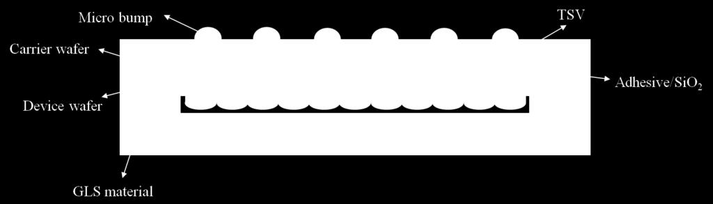
3 General Process Flow Coating/Bonding Backgrinding Stress relief etching Photolithography Plasma etching/rie Resist stripping 70-µm-thick wafer, 1:1-aspect-ratio vias, copper redistribution layer Dielectric deposition Seed layer deposition Electroplating Debonding Silicon interposer, RDL - Fuji

4 Development of Thin Wafer Handling Technology Brewer Science Bonding Material Carrier Thermal Bonding Thinning & Backside Processing Debonding Thermal Stability 300 C Heat 200 C 100 C Note. Carrier-less solutions are excluded
5 30 Development of Debonding Technologies WPH Gen 3 Gen 2 Gen 1 Gen 3 Thermal Stability 300 C Release Zone Stiction Zone 20 Slide Heat 200 C C


6 Brewer Science Thin Wafer Handling Technologies Carrier Preparation Coating Process Debonding BrewerBOND carrier preparation ZoneBOND carrier preparation Glass BrewerBOND materials ZoneBOND materials WaferBOND materials Glass Edge refortification Chemical resistance CVD stability Effective cleaning Carrier recycle Gen 3 tech ZoneBOND debonding Slide off Chemical release Sapphire Silicon Device


7 Requirements Temporary Bonding Must Meet Step Process Consideration Examples 1 Coating/ Carrier prep. 2 Bonding 3 Backside processes 4 Debonding TTV, coating uniformity, step coverage TTV, void free, alignment, squeeze out Void free, warpage With frame, room temperature debonding 5 Cleaning Residue free, high yield

8 Challenges Edge bead/ Uniformity Carrier TSV Wafer Bonding & Thinning Carrier In-film defect TSV Wafer Carrier Thinning Carrier Process compatibility Carrier Backside Processes Carrier


9 Coating Profile Spin Coating High edge bead from traditional spin coating Backgrinding performance is directly impacted For example, edge beads ~80 µm in height are typical Reduced by process and equipment advancements to 7 µm 80 µm 7 µm 14 mm from edge

10 Thinning with WaferBOND HT Bonding Material (IMEC)

11 Successful Thinning to 5 µm (ITRI Ad-STAC) 300-mm Blank Si 5-µm Si Glass Carrier


12 Process and Equipment Effect on Material Requirements Found stress pattern or wrinkling after PECVD Perceived as a material failure fixed by process and equipment changes Same bonding material, coating, and baking conditions PECVD at 160 C set point Wafer size: 300-mm Si
13 High Thermal Stability The newest formulation meets the high temperature requirements in backside process. - Decomposition temperature up to 363 C (2% weight loss measured by TGA in air) - Isothermal at 250 C for 30 minutes in air, no noticeable weight loss


14 High Thermal Stability Bonding at 200 C - No delamination after heat treatment at 260 C for 1 hour on a hot plate in air - No delamination after heat treatment at 300 C for 15 min under vacuum After bonding at 200 C After heat treatment at 260 C for 60 min After heat treatment at 300 C for 15 min


15 300-mm Wafer Bonding and Grinding Thickness: Devi 300-mm Si wafer µm Bonding material thickness µm Carrier µm Post-bonding TTV: 7.4 µm CSAM: as left image, no void Thinning: After Grinding Avg. Thickness of Si (µm) Pair Thickness (µm) Pair TTV (µm)
16 Summary Thin wafer handling is a necessity for advanced 3-D IC manufacturing Post-thinning TTV less than 2 µm can be achieved through selected bonding material and process control Optimization of bonding material and bonding process can eliminate defects Use of a proprietary BrewerBOND material with stability higher than 300 C can result in coating non-uniformity less than 5% and high WPH
17 Acknowledgements A special thank you to: IMEC ITRI Ad-STAC SUSS MicroTec SEMI Europa The Brewer Science development team

18 Where innovation takes flight! sm
Update in Material and Process Technologies for 2.5/3D IC Dr. Rainer Knippelmeyer CTO and VP R&D, SÜSS MicroTec AG
 Update in Material and Process Technologies for 2.5/3D IC Dr. Rainer Knippelmeyer CTO and VP R&D, SÜSS MicroTec AG TEMPORARY BONDING / DEBONDING AS THIN WAFER HANDLING SOLUTION FOR 3DIC & INTERPOSERS Device
1
 Process methodologies for temporary thin wafer handling solutions By Justin Furse, Technology Strategist, Brewer Science, Inc. Use of temporary bonding/debonding as part of thin wafer handling processes
Thin Wafer Handling Challenges and Emerging Solutions
 1 Thin Wafer Handling Challenges and Emerging Solutions Dr. Shari Farrens, Mr. Pete Bisson, Mr. Sumant Sood and Mr. James Hermanowski SUSS MicroTec, 228 Suss Drive, Waterbury Center, VT 05655, USA 2 Thin
LATEST INSIGHTS IN MATERIAL AND PROCESS TECHNOLOGIES FOR INTERPOSER AND 3D STACKING
 LATEST INSIGHTS IN MATERIAL AND PROCESS TECHNOLOGIES FOR INTERPOSER AND 3D STACKING European 3D TSV Summit, January 22-23, 2013, Grenoble Dr. Rainer Knippelmeyer, CTO and VP of R&D, GM Product Line Bonder
A Temporary Bonding and Debonding Technology for TSV Fabrication
 A Temporary Bonding and Debonding Technology for TSV Fabrication Taku Kawauchi, Masatoshi Shiraishi, Satoshi Okawa, Masahiro Yamamoto Tokyo Electron Ltd, Japan Taku Kawauchi, Tokyo Electron Ltd./Slide
Passionately Innovating With Customers To Create A Connected World
 Passionately Innovating With Customers To Create A Connected World Multi Die Integration Can Material Suppliers Meet the Challenge? Nov 14, 2012 Jeff Calvert - R&D Director, Advanced Packaging Technologies
Temporary Wafer Bonding - Key Technology for 3D-MEMS Integration
 Temporary Wafer Bonding - Key Technology for 3D-MEMS Integration 2016-06-15, Chemnitz Chemnitz University of Technology Basic Research Fraunhofer ENAS System-Packaging (SP) Back-End of Line (BEOL) Applied
EV Group. Enabling processes for 3D interposer. Dr. Thorsten Matthias EV Group
 EV Group Enabling processes for 3D interposer Dr. Thorsten Matthias EV Group EV Group in a Nutshell st Our philosophy Our mission in serving next generation application in semiconductor technology Equipment
XBC300 Gen2. Fully-automated debonder and Cleaner
 XBC300 Gen2 Fully-automated debonder and Cleaner XBC300 Gen2 FULLY AUTOMATED DEBONDER AND CLEANER The SUSS XBC300 Gen2 debonder and cleaner platform is designed for process development as well as high
A Novel Approach to TSV Metallization based on Electrografted Copper Nucleation Layers. Claudio Truzzi, PhD Chief Technology Officer Alchimer
 A Novel Approach to TSV Metallization based on Electrografted Copper Nucleation Layers Claudio Truzzi, PhD Chief Technology Officer Alchimer Overview Introduction Electrografting (eg) Technology Description
Hybrid Wafer Level Bonding for 3D IC
 Hybrid Wafer Level Bonding for 3D IC An Equipment Perspective Markus Wimplinger, Corporate Technology Development & IP Director History & Roadmap - BSI CIS Devices???? 2013 2 nd Generation 3D BSI CIS with
EV Group. Engineered Substrates for future compound semiconductor devices
 EV Group Engineered Substrates for future compound semiconductor devices Engineered Substrates HB-LED: Engineered growth substrates GaN / GaP layer transfer Mobility enhancement solutions: III-Vs to silicon
SHRINK. STACK. INTEGRATE.
 SHRINK. STACK. INTEGRATE. SUSS MICROTEC PRODUCT PORTFOLIO SHAPING THE FUTURE With more than 60 years of engineering experience SUSS MicroTec is a leading supplier of process equipment for microstructuring
OPTIMIZATION OF DIELECTRICS SURFACE PREPARATION FOR VACUUM COATING
 OPTIMIZATION OF DIELECTRICS SURFACE PREPARATION FOR VACUUM COATING Dr. Boris Statnikov Introduction Modern MICRO and NANO technologies in ultra- and high-frequency electronics are widely focused on application
Fiducial Marks for EUV mask blanks. Jan-Peter Urbach, James Folta, Cindy Larson, P.A. Kearney, and Thomas White
 Fiducial Marks for EUV mask blanks Jan-Peter Urbach, James Folta, Cindy Larson, P.A. Kearney, and Thomas White Fiducial marks are laser scribed on 200 mm wafers to enable defect registration on metrology
Advances in Back-side Via Etching of SiC for GaN Device Applications
 Advances in Back-side Via Etching of SiC for GaN Device Applications Anthony Barker, Kevin Riddell, Huma Ashraf & Dave Thomas SPTS Technologies, Ringland Way, Newport NP18 2TA, UK, dave.thomas@spts.com,
2017 IEEE 67th Electronic Components and Technology Conference
 2017 IEEE 67th Electronic Components and Technology Conference A Unique Temporary Bond Solution Based on a Polymeric Material Tacky at Room Temperature and Highly Thermally Resistant Application Extension
TCAD Modeling of Stress Impact on Performance and Reliability
 TCAD Modeling of Stress Impact on Performance and Reliability Xiaopeng Xu TCAD R&D, Synopsys March 16, 2010 SEMATECH Workshop on Stress Management for 3D ICs using Through Silicon Vias 1 Outline Introduction
MICROCHIP MANUFACTURING by S. Wolf
 by S. Wolf Chapter 15 ALUMINUM THIN-FILMS and SPUTTER-DEPOSITION 2004 by LATTICE PRESS CHAPTER 15 - CONTENTS Aluminum Thin-Films Sputter-Deposition Process Steps Physics of Sputter-Deposition Magnetron-Sputtering
1 INTRODUCTION 2 SAMPLE PREPARATIONS
 Chikage NORITAKE This study seeks to analyze the reliability of three-dimensional (3D) chip stacked packages under cyclic thermal loading. The critical areas of 3D chip stacked packages are defined using
Wafer Scale Homogeneous Bilayer Graphene Films by. Chemical Vapor Deposition
 Supporting Information for Wafer Scale Homogeneous Bilayer Graphene Films by Chemical Vapor Deposition Seunghyun Lee, Kyunghoon Lee, Zhaohui Zhong Department of Electrical Engineering and Computer Science,
EE143 LAB. Professor N Cheung, U.C. Berkeley
 EE143 LAB 1 1 EE143 Equipment in Cory 218 2 Guidelines for Process Integration * A sequence of Additive and Subtractive steps with lateral patterning Processing Steps Si wafer Watch out for materials compatibility
Alternative deposition solution for cost reduction of TSV integration
 Alternative deposition solution for cost reduction of TSV integration J. Vitiello, F. Piallat, L. Bonnet KOBUS 611 rue Aristide Bergès, Z.A. de Pré Millet, Montbonnot-Saint-Martin, 38330 France Ph: +33
Superconducting Ti/TiN thin films for mm wave absorption
 Superconducting /N thin films for mm wave absorption A.Aliane 1, M. Solana 2, V. Goudon 1, C. Vialle 1, S. Pocas 1, E. Baghe 1, L. Carle 1, W. Rabaud 1, L. Saminadayar 2, L. Dussopt 1, P.Agnese 1, N. Lio
Figure 1: Graphene release, transfer and stacking processes. The graphene stacking began with CVD
 Supplementary figure 1 Graphene Growth and Transfer Graphene PMMA FeCl 3 DI water Copper foil CVD growth Back side etch PMMA coating Copper etch in 0.25M FeCl 3 DI water rinse 1 st transfer DI water 1:10
Film Deposition Part 1
 1 Film Deposition Part 1 Chapter 11 : Semiconductor Manufacturing Technology by M. Quirk & J. Serda Spring Semester 2013 Saroj Kumar Patra Semidonductor Manufacturing Technology, Norwegian University of
CURRENT STATUS OF NANOIMPRINT LITHOGRAPHY DEVELOPMENT IN CNMM
 U.S. -KOREA Forums on Nanotechnology 1 CURRENT STATUS OF NANOIMPRINT LITHOGRAPHY DEVELOPMENT IN CNMM February 17 th 2005 Eung-Sug Lee,Jun-Ho Jeong Korea Institute of Machinery & Materials U.S. -KOREA Forums
ALIGNMENT ACCURACY IN A MA/BA8 GEN3 USING SUBSTRATE CONFORMAL IMPRINT LITHOGRAPHY (SCIL)
") ALIGNMENT ACCURACY IN A MA/BA8 GEN3 USING SUBSTRATE CONFORMAL IMPRINT LITHOGRAPHY (SCIL) Robert Fader Fraunhofer Institute for Integrated Systems and Device Technology (IISB) Germany Ulrike Schömbs SUSS
ALIGNMENT ACCURACY IN A MA/BA8 GEN3 USING SUBSTRATE CONFORMAL IMPRINT LITHOGRAPHY (SCIL) Robert Fader Fraunhofer Institute for Integrated Systems and Device Technology (IISB) Germany Ulrike Schömbs SUSS
Self-study problems and questions Processing and Device Technology, FFF110/FYSD13
 Self-study problems and questions Processing and Device Technology, FFF110/FYSD13 Version 2016_01 In addition to the problems discussed at the seminars and at the lectures, you can use this set of problems
Carrier Transport by Diffusion
 Carrier Transport by Diffusion Holes diffuse ÒdownÓ the concentration gradient and carry a positive charge --> hole diffusion current has the opposite sign to the gradient in hole concentration dp/dx p(x)
FRAUNHOFER INSTITUTE FOR SURFACE ENGINEERING AND THIN FILMS IST ATMOSPHERIC PRESSURE PLASMA PROCESSES
 FRAUNHOFER INSTITUTE FOR SURFACE ENGINEERING AND THIN FILMS IST ATMOSPHERIC PRESSURE PLASMA PROCESSES 1 2 ATMOSPHERIC PRESSURE PLASMA PROCESSES AT THE FRAUNHOFER IST Today, atmospheric pressure plasma
Superconducting Through-Silicon Vias for Quantum Integrated Circuits
 Superconducting Through-Silicon Vias for Quantum Integrated Circuits Mehrnoosh Vahidpour, William O Brien, Jon Tyler Whyland, Joel Angeles, Jayss Marshall, Diego Scarabelli, Genya Crossman, Kamal Yadav,
CVD-3 LFSIN SiN x Process
 CVD-3 LFSIN SiN x Process Top Electrode, C Bottom Electrode, C Pump to Base Time (s) SiH 4 Flow Standard LFSIN Process NH 3 Flow N 2 HF (watts) LF (watts) Pressure (mtorr Deposition Time min:s.s Pump to
UNIVERSITY OF CALIFORNIA College of Engineering Department of Electrical Engineering and Computer Sciences. Fall Exam 1
 UNIVERSITY OF CALIFORNIA College of Engineering Department of Electrical Engineering and Computer Sciences EECS 143 Fall 2008 Exam 1 Professor Ali Javey Answer Key Name: SID: 1337 Closed book. One sheet
VACUUM TECHNOLOGIES NEEDED FOR 3D DEVICE PROCESSING
 VACUUM TECHNOLOGIES NEEDED FOR 3D DEVICE PROCESSING Future ICs will use more 3D device structures such as finfets and gate-all-around (GAA) transistors, and so vacuum deposition processes are needed that
Case Study of Electronic Materials Packaging with Poor Metal Adhesion and the Process for Performing Root Cause Failure Analysis
 Case Study of Electronic Materials Packaging with Poor Metal Adhesion and the Process for Performing Root Cause Failure Analysis Dr. E. A. Leone BACKGRUND ne trend in the electronic packaging industry
SCI. Scientific Computing International. Scientific Computing International. FilmTek. Raising Thin Film Metrology Performance to a New Level
 FilmTek Raising Thin Film Metrology Performance to a New Level 1 Through Silicon Via (TSV) Metrology FilmTek TM TM TSV TSV Metrology Advantages Measure high aspect ratio TSV structures (up to 30:1) Measure
Multilayer Wiring Technology with Grinding Planarization of Dielectric Layer and Via Posts
 Tani et al.: Multilayer Wiring Technology with Grinding Planarization (1/6) [Technical Paper] Multilayer Wiring Technology with Grinding Planarization of Dielectric Layer and Via Posts Motoaki Tani, Kanae
A Cost and Yield Analysis of Wafer-to-wafer Bonding. Amy Palesko SavanSys Solutions LLC
 A Cost and Yield Analysis of Wafer-to-wafer Bonding Amy Palesko amyp@savansys.com SavanSys Solutions LLC Introduction When a product requires the bonding of two wafers or die, there are a number of methods
A Temporary Bonding and Debonding Technology for TSV Fabrication. Masahiro Yamamoto TEL 3DI Dept. ATS BU
 A Temporary Bonding and Debonding Technology for TSV Fabrication Masahiro Yamamoto TEL 3DI Dept. ATS BU Contents About TEL Temporary Bonder Debonder Process Trends Bonder/Debonder System Outlook Summary
Micro/nano and precision manufacturing technologies and applications
 The 4th China-American Frontiers of Engineering Symposium Micro/nano and precision manufacturing technologies and applications Dazhi Wang School of Mechanical Engineering Dalian University of Technology
IC Fabrication Technology
 IC Fabrication Technology * History: 1958-59: J. Kilby, Texas Instruments and R. Noyce, Fairchild * Key Idea: batch fabrication of electronic circuits n entire circuit, say 10 7 transistors and 5 levels
CVD-3 SIO-HU SiO 2 Process
 CVD-3 SIO-HU SiO 2 Process Top Electrode, C Bottom Electrode, C Pump to Base Time (s) SiH 4 Flow Standard SIO-HU Process N 2 O Flow N 2 HF (watts) LF (watts) Pressure (mtorr Deposition Time min:s.s Pump
TEST REPORT (Self-Tested Data)
") TEST REPORT (Self-Tested Data) CLIENT: IPC Validation Services 3000 Lakeside Drive Suite 105N Bannockburn, IL 60015 USA Attention: Mr. Randy Cherry +1-847-597-5606 TEST ITEMS: Peel Strength, Volume Resistivity,
TEST REPORT (Self-Tested Data) CLIENT: IPC Validation Services 3000 Lakeside Drive Suite 105N Bannockburn, IL 60015 USA Attention: Mr. Randy Cherry +1-847-597-5606 TEST ITEMS: Peel Strength, Volume Resistivity,
CVD: General considerations.
 CVD: General considerations. PVD: Move material from bulk to thin film form. Limited primarily to metals or simple materials. Limited by thermal stability/vapor pressure considerations. Typically requires
Chapter 10 3D Integration Based upon Dielectric Adhesive Bonding
 Chapter 10 3D Integration Based upon Dielectric Adhesive Bonding Jian-Qiang Lu, Timothy S. Cale, and Ronald J. Gutmann 10.1 Introduction Wafer bonding with intermediate polymer adhesives is one of the
percolating nanotube networks
 Supporting Information for: A highly elastic, capacitive strain gauge based on percolating nanotube networks 0.2 0.18 0.16 0.14 Force (kgf) 0.12 0.1 0.08 0.06 0.04 0.02 Raw Data Mooney-Rivlin (R 2 =0.996)
Fast Bonding of Substrates for the Formation of Microfluidic Channels at Room Temperature
 Supplementary Material (ESI) for Lab on a Chip This journal is The Royal Society of Chemistry 2005 Supporting Information Fast Bonding of Substrates for the Formation of Microfluidic Channels at Room Temperature
Thermo-structural Model of Stacked Field-programmable Gate Arrays (FPGAs) with Through-silicon Vias (TSVs)
 with Through-silicon Vias (TSVs)") Manuscript for Review Thermo-structural Model of Stacked Field-programmable Gate Arrays (FPGAs) with Through-silicon Vias (TSVs) Journal: Electronics Letters Manuscript ID: draft Manuscript Type: Letter
Manuscript for Review Thermo-structural Model of Stacked Field-programmable Gate Arrays (FPGAs) with Through-silicon Vias (TSVs) Journal: Electronics Letters Manuscript ID: draft Manuscript Type: Letter
Plasma Deposition (Overview) Lecture 1
 Lecture 1") Plasma Deposition (Overview) Lecture 1 Material Processes Plasma Processing Plasma-assisted Deposition Implantation Surface Modification Development of Plasma-based processing Microelectronics needs (fabrication
Plasma Deposition (Overview) Lecture 1 Material Processes Plasma Processing Plasma-assisted Deposition Implantation Surface Modification Development of Plasma-based processing Microelectronics needs (fabrication
Research and Development of Parylene Thin-Film Deposition and Application for Water-Proofing
 Advanced Materials Research Online: 2012-06-14 ISSN: 1662-8985, Vols. 538-541, pp 23-28 doi:10.4028/www.scientific.net/amr.538-541.23 2012 Trans Tech Publications, Switzerland Research and Development
CVD-3 MFSIN-HU-2 SiN x Mixed Frequency Process
 CVD-3 MFSIN-HU-2 SiN x Mixed Frequency Process Standard MFSIN-HU-2 Process Top C Bottom C Pump to Base Time (s) SiH 4 Flow HF/ LF NH 3 Flow HF/LF N 2 HF/LF HF (watts) LF (watts) HF Time LF Time Pressure
Supporting Information
 Supporting Information Real-Time Monitoring of Insulin Using a Graphene Field-Effect Transistor Aptameric Nanosensor Zhuang Hao, a,b Yibo Zhu, a Xuejun Wang, a Pavana G. Rotti, c,d Christopher DiMarco,
Chapter 3 : ULSI Manufacturing Technology - (c) Photolithography
 Photolithography") Chapter 3 : ULSI Manufacturing Technology - (c) Photolithography 1 Reference 1. Semiconductor Manufacturing Technology : Michael Quirk and Julian Serda (2001) 2. - (2004) 3. Semiconductor Physics and Devices-
Chapter 3 : ULSI Manufacturing Technology - (c) Photolithography 1 Reference 1. Semiconductor Manufacturing Technology : Michael Quirk and Julian Serda (2001) 2. - (2004) 3. Semiconductor Physics and Devices-
Electrografted insulator layer as copper diffusion barrier for TSV interposers
 Electrografted insulator layer as copper diffusion barrier for TSV interposers V. Mevellec, D. Suhr, T. Dequivre, P. Blondeau, L. Religieux and F. Raynal Scottsdale/Fountain Hills March 12-14, 2013 3D
CVD-3 MFSIN-HU-1 SiN x Mixed Frequency Process
 CVD-3 MFSIN-HU-1 SiN x Mixed Frequency Process Standard MFSIN-HU-1 Process Top C Bottom C Pump to Base Time (s) SiH 4 Flow HF/ LF NH 3 Flow HF/LF N 2 HF/LF HF (watts) LF (watts) HF Time LF Time Pressure
A Novel Approach to the Layer Number-Controlled and Grain Size- Controlled Growth of High Quality Graphene for Nanoelectronics
 Supporting Information A Novel Approach to the Layer Number-Controlled and Grain Size- Controlled Growth of High Quality Graphene for Nanoelectronics Tej B. Limbu 1,2, Jean C. Hernández 3, Frank Mendoza
ELECTROMAGNETIC MODELING OF THREE DIMENSIONAL INTEGRATED CIRCUITS MENTOR GRAPHICS
 ELECTROMAGNETIC MODELING OF THREE DIMENSIONAL INTEGRATED CIRCUITS MENTOR GRAPHICS H I G H S P E E D D E S I G N W H I T E P A P E R w w w. m e n t o r. c o m / p c b INTRODUCTION Three Dimensional Integrated
Chapter 7 Plasma Basic
 Chapter 7 Plasma Basic Hong Xiao, Ph. D. hxiao89@hotmail.com www2.austin.cc.tx.us/hongxiao/book.htm Hong Xiao, Ph. D. www2.austin.cc.tx.us/hongxiao/book.htm 1 Objectives List at least three IC processes
Fabrication Technology, Part I
 EEL5225: Principles of MEMS Transducers (Fall 2004) Fabrication Technology, Part I Agenda: Microfabrication Overview Basic semiconductor devices Materials Key processes Oxidation Thin-film Deposition Reading:
Recent Advances and Challenges in Nanoparticle Monitoring for the Semiconductor Industry. December 12, 2013
 Recent Advances and Challenges in Nanoparticle Monitoring for the Semiconductor Industry December 12, 2013 Agenda Introduction Wafer Environment Nano-Contamination Requirements State-of-the-Art Monitoring
Y. C. Lee. Micro-Scale Engineering I Microelectromechanical Systems (MEMS)
") Micro-Scale Engineering I Microelectromechanical Systems (MEMS) Y. C. Lee Department of Mechanical Engineering University of Colorado Boulder, CO 80309-0427 leeyc@colorado.edu January 15, 2014 1 Contents
Micro-Scale Engineering I Microelectromechanical Systems (MEMS) Y. C. Lee Department of Mechanical Engineering University of Colorado Boulder, CO 80309-0427 leeyc@colorado.edu January 15, 2014 1 Contents
Supplementary Information
 ature anotechnology reference number: AO-06110617A Growth and alignment of polyaniline nanofibres with superhydrophobic, superhydrophilic and other properties an-rong Chiou 1,2,3, Chunmeng Lu 1, Jingjiao
Lecture 0: Introduction
 Lecture 0: Introduction Introduction q Integrated circuits: many transistors on one chip q Very Large Scale Integration (VLSI): bucketloads! q Complementary Metal Oxide Semiconductor Fast, cheap, low power
CHARACTERIZATION OF DEEP REACTIVE ION ETCHING (DRIE) PROCESS FOR ELECTRICAL THROUGH-WAFER INTERCONNECTS FOR PIEZORESISTIVE INERTIAL SENSORS
 PROCESS FOR ELECTRICAL THROUGH-WAFER INTERCONNECTS FOR PIEZORESISTIVE INERTIAL SENSORS") CHARACTERIZATION OF DEEP REACTIVE ION ETCHING (DRIE) PROCESS FOR ELECTRICAL THROUGH-WAFER INTERCONNECTS FOR PIEZORESISTIVE INERTIAL SENSORS Maria Suggs, Physics Major, Southern Polytechnic State University
CHARACTERIZATION OF DEEP REACTIVE ION ETCHING (DRIE) PROCESS FOR ELECTRICAL THROUGH-WAFER INTERCONNECTS FOR PIEZORESISTIVE INERTIAL SENSORS Maria Suggs, Physics Major, Southern Polytechnic State University
BONDING PARAMETERS OPTIMIZATION IN LOW TEMPERATURE ADHESIVE WAFER BONDING PROCESS USING SU-8 AS AN INTERMEDIATE ADHESIVE LAYER
 BONDING PARAMETERS OPTIMIZATION IN LOW TEMPERATURE ADHESIVE WAFER BONDING PROCESS USING SU-8 AS AN INTERMEDIATE ADHESIVE LAYER Srinivasulu Korrapati B.E., Anna University, India, 2005 PROJECT Submitted
Graphene films on silicon carbide (SiC) wafers supplied by Nitride Crystals, Inc.
 wafers supplied by Nitride Crystals, Inc.") 9702 Gayton Road, Suite 320, Richmond, VA 23238, USA Phone: +1 (804) 709-6696 info@nitride-crystals.com www.nitride-crystals.com Graphene films on silicon carbide (SiC) wafers supplied by Nitride Crystals,
9702 Gayton Road, Suite 320, Richmond, VA 23238, USA Phone: +1 (804) 709-6696 info@nitride-crystals.com www.nitride-crystals.com Graphene films on silicon carbide (SiC) wafers supplied by Nitride Crystals,
Supplementary Figure 1 Detailed illustration on the fabrication process of templatestripped
 Supplementary Figure 1 Detailed illustration on the fabrication process of templatestripped gold substrate. (a) Spin coating of hydrogen silsesquioxane (HSQ) resist onto the silicon substrate with a thickness
Supplementary Figure 1: Micromechanical cleavage of graphene on oxygen plasma treated Si/SiO2. Supplementary Figure 2: Comparison of hbn yield.
 1 2 3 4 Supplementary Figure 1: Micromechanical cleavage of graphene on oxygen plasma treated Si/SiO 2. Optical microscopy images of three examples of large single layer graphene flakes cleaved on a single
Scaling up Chemical Vapor Deposition Graphene to 300 mm Si substrates
 Scaling up Chemical Vapor Deposition Graphene to 300 mm Si substrates Co- Authors Aixtron Alex Jouvray Simon Buttress Gavin Dodge Ken Teo The work shown here has received partial funding from the European
Wireless Sensor Networks. Picocube
 Wireless Sensor Networks Low Power Radio Power Storage Sensor Renewable Power Picocube Supply Vibrational Energy Scavenging Nathan Emley DRETD TAC Meeting February 19, 2008 Vibrational Scavenger Team:
Supporting Information. Direct Growth of Graphene Films on 3D Grating. Structural Quartz Substrates for High-performance. Pressure-Sensitive Sensor
 Supporting Information Direct Growth of Graphene Films on 3D Grating Structural Quartz Substrates for High-performance Pressure-Sensitive Sensor Xuefen Song, a,b Tai Sun b Jun Yang, b Leyong Yu, b Dacheng
Pattern Transfer- photolithography
 Pattern Transfer- photolithography DUV : EUV : 13 nm 248 (KrF), 193 (ArF), 157 (F 2 )nm H line: 400 nm I line: 365 nm G line: 436 nm Wavelength (nm) High pressure Hg arc lamp emission Ref: Campbell: 7
Taurus-Topography. Topography Modeling for IC Technology
 SYSTEMS PRODUCTS LOGICAL PRODUCTS PHYSICAL IMPLEMENTATION SIMULATION AND ANALYSIS LIBRARIES TCAD Aurora DFM WorkBench Davinci Medici Raphael Raphael-NES Silicon Early Access TSUPREM-4 Taurus-Device Taurus-Lithography
Supplementary Information Our InGaN/GaN multiple quantum wells (MQWs) based one-dimensional (1D) grating structures
 based one-dimensional (1D) grating structures") Polarized white light from hybrid organic/iii-nitrides grating structures M. Athanasiou, R. M. Smith, S. Ghataora and T. Wang* Department of Electronic and Electrical Engineering, University of Sheffield,
Polarized white light from hybrid organic/iii-nitrides grating structures M. Athanasiou, R. M. Smith, S. Ghataora and T. Wang* Department of Electronic and Electrical Engineering, University of Sheffield,
An Investigation on NEG Thick Film for Vacuum packaging of MEMS
 An Investigation on NEG Thick Film for Vacuum packaging of MEMS Y.F. Jin* 1,3, Z.P. Wang 1, L. Zhao 2, P.C. Lim 1, J. Wei 1 1) Singapore Institute of Manufacturing Technology, 71 Nanyang Drive, Singapore
Technology for Micro- and Nanostructures Micro- and Nanotechnology
 Lecture 10: Deposition Technology for Micro- and Nanostructures Micro- and Nanotechnology Peter Unger mailto: peter.unger @ uni-ulm.de Institute of Optoelectronics University of Ulm http://www.uni-ulm.de/opto
Carbon Nanotubes for Interconnect Applications Franz Kreupl, Andrew P. Graham, Maik Liebau, Georg S. Duesberg, Robert Seidel, Eugen Unger
 Carbon Nanotubes for Interconnect Applications Franz Kreupl, Andrew P. Graham, Maik Liebau, Georg S. Duesberg, Robert Seidel, Eugen Unger Infineon Technologies Corporate Research Munich, Germany Outline
Microfabrication for MEMS: Part I
 Microfabrication for MEMS: Part I Carol Livermore Massachusetts Institute of Technology * With thanks to Steve Senturia, from whose lecture notes some of these materials are adapted. CL: 6.777J/2.372J
EE C245 ME C218 Introduction to MEMS Design Fall 2007
 EE C245 ME C218 Introduction to MEMS Design Fall 2007 Prof. Clark T.-C. Nguyen Dept. of Electrical Engineering & Computer Sciences University of California at Berkeley Berkeley, CA 94720 Lecture 4: Film
All-Chemical-Solution Coated Conductors at Deutsche Nanoschicht GmbH
 chemistry meets energy All-Chemical-Solution Coated Conductors at Deutsche Nanoschicht GmbH Michael Baecker; Martina Falter; Ron Feenstra; Brygida Wojtyniak; Jan Bennewitz; Jan Kunert; Mark O. Rikel Deutsche
custom reticle solutions
 custom reticle solutions 01 special micro structures Pyser Optics has over 60 years experience in producing high quality micro structure products. These products are supplied worldwide to industries including
Nanocarbon Interconnects - From 1D to 3D
 Nanocarbon Interconnects - From 1D to 3D Cary Y. Yang Santa Clara University Outline Introduction CNT as 1D interconnect structure CNT-graphene as all-carbon 3D interconnect Summary Device Scaling driven
Wet Chemical Processing with Megasonics Assist for the Removal of Bumping Process Photomasks
 Wet Chemical Processing with Megasonics Assist for the Removal of Bumping Process Photomasks Hongseong Sohn and John Tracy Akrion Systems 6330 Hedgewood Drive, Suite 150 Allentown, PA 18106, USA Abstract
Objective: Competitive Low-Cost Thin-Film Varactor Technology. Integrated Monolithic Capacitors using Sputtered/MOCVD material on low-cost substrates
 Overview of Program Objective: Competitive Low-Cost Thin-Film Varactor Technology coplanar waveguide (CPW) capacitor ground signal ground Si substrate etched troughs Focus of Our Program! Reproducibility!
EN2912C: Future Directions in Computing Lecture 08: Overview of Near-Term Emerging Computing Technologies
 EN2912C: Future Directions in Computing Lecture 08: Overview of Near-Term Emerging Computing Technologies Prof. Sherief Reda Division of Engineering Brown University Fall 2008 1 Near-term emerging computing
Technology Brief 9: Capacitive Sensors
 218 TEHNOLOGY BRIEF 9: APAITIVE SENSORS Technology Brief 9: apacitive Sensors To sense is to respond to a stimulus. (See Tech Brief 7 on resistive sensors.) A capacitor can function as a sensor if the
Dan Smith 2016 EUV Mask Pellicle TWG San Jose CA 21 Feb 2016
 ASML NXE Pellicle progress update Dan Smith 2016 EUV Mask Pellicle TWG San Jose CA 21 Feb 2016 Contents Slide 2 Introduction: a look back at 2015 NXE Pellicle update Pellicle film development NXE Scanner
Immersed diffraction gratings for the Sentinel-5 earth observation mission. Ralf Kohlhaas
 Immersed diffraction gratings for the Sentinel-5 earth observation mission Ralf Kohlhaas 10-10-2017 Introduction SRON supports earth observation satellite missions with the delivery of immersed diffraction
Supporting Information
 Electronic Supplementary Material (ESI) for ChemComm. This journal is The Royal Society of Chemistry 2014 Supporting Information Controllable Atmospheric Pressure Growth of Mono-layer, Bi-layer and Tri-layer
F R A U N H O F E R I N
 FRAUNHOFER Institute FoR Electronic NAno systems ENAS System Packaging 1 2 3 4 5 The actual developments of micro and nano technologies are fascinating. Undoubted they are playing a key role in today s
MEEN Nanoscale Issues in Manufacturing. Lithography Lecture 1: The Lithographic Process
 MEEN 489-500 Nanoscale Issues in Manufacturing Lithography Lecture 1: The Lithographic Process 1 Discuss Reading Assignment 1 1 Introducing Nano 2 2 Size Matters 3 3 Interlude One-The Fundamental Science
Lithography and Etching
 Lithography and Etching Victor Ovchinnikov Chapters 8.1, 8.4, 9, 11 Previous lecture Microdevices Main processes: Thin film deposition Patterning (lithography) Doping Materials: Single crystal (monocrystal)
SUPPLEMENTARY FIGURES
 SUPPLEMENTARY FIGURES a b c Supplementary Figure 1 Fabrication of the near-field radiative heat transfer device. a, Main fabrication steps for the bottom Si substrate. b, Main fabrication steps for the
EE 527 MICROFABRICATION. Lecture 25 Tai-Chang Chen University of Washington
 EE 527 MICROFABRICATION Lecture 25 Tai-Chang Chen University of Washington ION MILLING SYSTEM Kaufmann source Use e-beam to strike plasma A magnetic field applied to increase ion density Drawback Low etch
Lecture 150 Basic IC Processes (10/10/01) Page ECE Analog Integrated Circuits and Systems P.E. Allen
 Page ECE Analog Integrated Circuits and Systems P.E. Allen") Lecture 150 Basic IC Processes (10/10/01) Page 1501 LECTURE 150 BASIC IC PROCESSES (READING: TextSec. 2.2) INTRODUCTION Objective The objective of this presentation is: 1.) Introduce the fabrication of
Lecture 150 Basic IC Processes (10/10/01) Page 1501 LECTURE 150 BASIC IC PROCESSES (READING: TextSec. 2.2) INTRODUCTION Objective The objective of this presentation is: 1.) Introduce the fabrication of
Supporting Information. Fast Synthesis of High-Performance Graphene by Rapid Thermal Chemical Vapor Deposition
 1 Supporting Information Fast Synthesis of High-Performance Graphene by Rapid Thermal Chemical Vapor Deposition Jaechul Ryu, 1,2, Youngsoo Kim, 4, Dongkwan Won, 1 Nayoung Kim, 1 Jin Sung Park, 1 Eun-Kyu
Post Tungsten CMP Cleaner Development with Improved Organic and Particle Residue Removal on Silicon Nitride and Excellent Tungsten Compatibility
 Post Tungsten CMP Cleaner Development with Improved Organic and Particle Residue Removal on Silicon Nitride and Excellent Tungsten Compatibility Ching-Hsun Chao, Chi Yen, Ping Hsu, Eugene Lee, Paul Bernatis
Reliability of 3D IC with Via-Middle TSV: Characterization and Modeling
 Reliability of 3D IC with Via-Middle TSV: Characterization and Modeling Victor Moroz *, Munkang Choi *, Geert Van der Plas, Paul Marchal, Kristof Croes, and Eric Beyne * Motivation: Build Reliable 3D IC