True Room Temperature Bonding a novel process for the creation of health tech consumables ATB. ir. Richard Bijlard Technogation - Invenios
|
|
|
- Elijah Blake
- 5 years ago
- Views:
Transcription

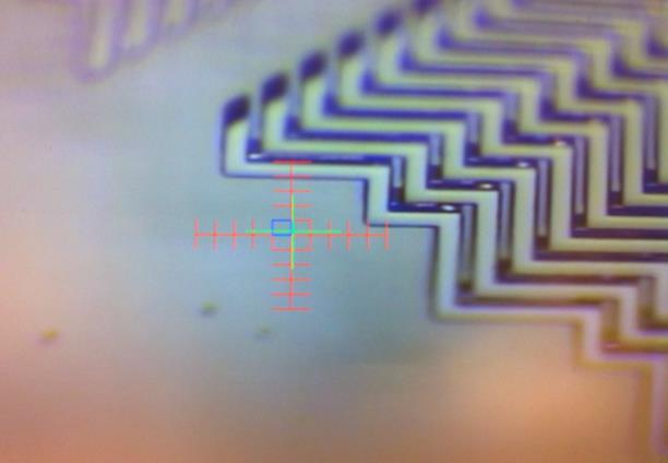
1 True Room Temperature Bonding a novel process for the creation of health tech consumables ATB ir. Richard Bijlard Technogation - Invenios Technogation Invenios Dec 2014
2 Presentation Overview Invenios Group From Lab to POC Challenges at creating advanced consumables ATB (True Room Temperature Bonding) Applications

")


3 Invenios Worldwide Langen (Hessen) Germany Santa Barbara, California, USA Eindhoven Netherlands


4 Health Tech Trends: from Lab to POC Laboratory: Large degree of freedom, versatile, high-end Stationary, expensive, specialist-use..


5 Lab-On-a-Chip Select necessary functionalities for test Shrink in size and in price! possible to scale down? absolutely necessary? combination possible? controllable -> pre-programmed! inputs and outputs? unambiguous interpretation of results! reproducible? mass-producible? low cost?

6 Some necessary L-O-C functions I/O sample intake: capillary, active pump, process sequence control: valves,.. reagent availability: pre-loaded / externally connected Heating/cooling electrodes? fluid? Measurement / readout sample processing: separation? chemical / electical / optical on-chip, external display,


7 And if you do it right, you get a solution that is: Very portable! (true Point-of-care solution) Cheap (uses less reagents, sample..) Fast Easy-to-use Safe

8 Design & Construction of Consumables Base material: Paper: very cheap! Plastic: cheap, easy to process Glass: transparancy, low autofluorescence, thermally stable, resistant against solvents Silicon: very mature semiconductor processes and tools available Construction: depends on material(s) ideal situation: combine materials! application dictates formfactor. the smaller, the better! (cheaper, portable,..!) FOTURAN PSGC


9 Pre-loaded Consumables / Sensors Problem - Need to have locally coated/functionalised structures but chip needs to be hermetically closed - Glueing introduces toxicity - Anodic Bonding and Diffusion Bonding are NOT options:
 Thin film blocking layer on interface No glue or high temperatures Appropriate wavelength laser Very locally created plasma, so bulk of the material stays")
10 Ambient (Room) Temperature Bonding (patented) (->2) True Room temperature < 30 o C (->1) Two or more substrates (different CTEs possible!) Thin film blocking layer on interface No glue or high temperatures Appropriate wavelength laser Very locally created plasma, so bulk of the material stays at room temperature
11 Room Temperature Bonding - Characteristics High bond strength > strength of the base material Low temperatures, heat impacted zone < 1 µm of bond joint Possible to create electrical leads in the same process step Embed fluids or biomaterial/-coatings (Fibronectin, Poly-acrylamide gel, PFTE / Teflon, ) Seals hermetically and in a vacuum, inert gas or even under water, if required Scalable process, designed for operating in clean room production lines

12 What can you bond? The following substrates can be bonded together in any combination: Several types of Glasses Quartz/Fuzed Silica Sapphire Silicon Silicon Nitride Silicon Oxide Metals (Gold, Titanium, ) Several plastics
13 Properties Comparison DIFFUSION ANODIC ADHESIVE Ambient Temperature (ATB ) High bond stability X X X Simple, low-cost process Surface Prep X X? X Applicable for materials with mismatched CTE s X X Chemically resistant? X Hermetically seals X X High transparency X X Temperature stable X Proprietary X Bonds in a vacuum X X X
14 DNA sequencing Chips, Lab-on-a-chip Dispensing Cancer Research Chip Electrofluidic lens

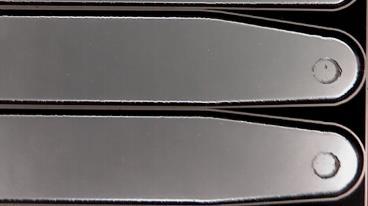
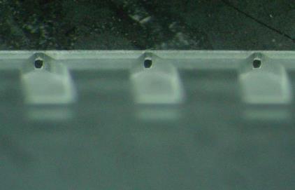
15 Application: Pressure Control Valve Made of glass Opening controlled by reference pressure Wavefront guides prevent bubbles Passive, implantable Very durable


16 Pressure Control Valve
17 Conclusions Trend towards Point Of Care requires small, smart and dedicated solutions All materials have pros and cons. advanced consumables combine best properties ATB enables connection of multiple materials on room temperature and does not harm biocoatings or materials
 phone: 06-4759 4741 email:")
18 Thank you for your attention! Richard Bijlard Business Development Europe Technogation (an Invenios company) phone: Technogation Invenios Dec 2014
Hybrid Wafer Level Bonding for 3D IC
 Hybrid Wafer Level Bonding for 3D IC An Equipment Perspective Markus Wimplinger, Corporate Technology Development & IP Director History & Roadmap - BSI CIS Devices???? 2013 2 nd Generation 3D BSI CIS with
Lecture 18: Microfluidic MEMS, Applications
 MECH 466 Microelectromechanical Systems University of Victoria Dept. of Mechanical Engineering Lecture 18: Microfluidic MEMS, Applications 1 Overview Microfluidic Electrokinetic Flow Basic Microfluidic
Nanotechnology Fabrication Methods.
 Nanotechnology Fabrication Methods. 10 / 05 / 2016 1 Summary: 1.Introduction to Nanotechnology:...3 2.Nanotechnology Fabrication Methods:...5 2.1.Top-down Methods:...7 2.2.Bottom-up Methods:...16 3.Conclusions:...19
Page Films. we support your innovation
 Page Films we support your innovation Page Films SAES Thin Film Technology: the Evolution of the Getter Integration Pioneering the development of getter technology, the SAES Getters Group is the world
The solution for all of your
 The solution for all of your nanoparticle sizing and zeta potential needs. DelsaNano Series Blood Banking Capillary Electrophoresis Cell Analysis Centrifugation Genomics Lab Automation Lab Tools Particle
White Paper: Transparent High Dielectric Nanocomposite
 Zhiyun (Gene) Chen, Ph.D., Vice President of Engineering Pixelligent Technologies 64 Beckley Street, Baltimore, Maryland 2224 Email: zchen@pixelligent.com February 205 Abstract High dielectric constant
SurPASS. Electrokinetic Analyzer for Solid Samples. ::: Innovation in Materials Science
 SurPASS Electrokinetic Analyzer for Solid Samples ::: Innovation in Materials Science SurPASS For Solid Surface Analysis The SurPASS electrokinetic analyzer helps material scientists to improve surface
OPTI510R: Photonics. Khanh Kieu College of Optical Sciences, University of Arizona Meinel building R.626
 OPTI510R: Photonics Khanh Kieu College of Optical Sciences, University of Arizona kkieu@optics.arizona.edu Meinel building R.626 Announcements HW#3 is assigned due Feb. 20 st Mid-term exam Feb 27, 2PM
Accelerated Neutral Atom Beam (ANAB)
") Accelerated Neutral Atom Beam (ANAB) Development and Commercialization July 2015 1 Technological Progression Sometimes it is necessary to develop a completely new tool or enabling technology to meet future
Accelerated Neutral Atom Beam (ANAB) Development and Commercialization July 2015 1 Technological Progression Sometimes it is necessary to develop a completely new tool or enabling technology to meet future
An Investigation on NEG Thick Film for Vacuum packaging of MEMS
 An Investigation on NEG Thick Film for Vacuum packaging of MEMS Y.F. Jin* 1,3, Z.P. Wang 1, L. Zhao 2, P.C. Lim 1, J. Wei 1 1) Singapore Institute of Manufacturing Technology, 71 Nanyang Drive, Singapore
SCB10H Series Pressure Elements PRODUCT FAMILY SPEFICIFATION. Doc. No B
 PRODUCT FAMILY SPEFICIFATION SCB10H Series Pressure Elements SCB10H Series Pressure Elements Doc. No. 82 1250 00 B Table of Contents 1 General Description... 3 1.1 Introduction... 3 1.2 General Description...
Plasma Deposition (Overview) Lecture 1
 Lecture 1") Plasma Deposition (Overview) Lecture 1 Material Processes Plasma Processing Plasma-assisted Deposition Implantation Surface Modification Development of Plasma-based processing Microelectronics needs (fabrication
Plasma Deposition (Overview) Lecture 1 Material Processes Plasma Processing Plasma-assisted Deposition Implantation Surface Modification Development of Plasma-based processing Microelectronics needs (fabrication
Biochemistry. Biochemical Techniques HPLC
 Description of Module Subject Name Paper Name 12 Module Name/Title 13 1. Objectives 1.1. To understand the basic concept and principle of 1.2. To understand the components and techniques of 1.3. To know
DEPOSITION OF THIN TiO 2 FILMS BY DC MAGNETRON SPUTTERING METHOD
 Chapter 4 DEPOSITION OF THIN TiO 2 FILMS BY DC MAGNETRON SPUTTERING METHOD 4.1 INTRODUCTION Sputter deposition process is another old technique being used in modern semiconductor industries. Sputtering
AC-829A. Issued on Apr. 15 th 2013 (Version 1.0)
") Hitachi Chemical Co., Ltd. Hitachi Anisotropic Conductive Film ANISOLM AC-829A Issued on Apr. 15 th 2013 (Version 1.0) 1. Standard specification, bonding condition, storage condition and characteristic.....1
Hitachi Chemical Co., Ltd. Hitachi Anisotropic Conductive Film ANISOLM AC-829A Issued on Apr. 15 th 2013 (Version 1.0) 1. Standard specification, bonding condition, storage condition and characteristic.....1
Chemie en Technologie van Materialen (Materials Science and Technology)
") ST module 8b Chemie en Technologie van Materialen (Materials Science and Technology) 2018-19 201600135 Module coordinator: dr.ir. Evert Houwman Chemie en Technologie van Materialen Materials Science and
ST module 8b Chemie en Technologie van Materialen (Materials Science and Technology) 2018-19 201600135 Module coordinator: dr.ir. Evert Houwman Chemie en Technologie van Materialen Materials Science and
The molecules that will be studied with this device will have an overall charge of
 The Basics of the Rotation of Polarized Light The molecules that will be studied with this device will have an overall charge of zero but will have localized polarities that can be used to orient the molecule.
Temporary Wafer Bonding - Key Technology for 3D-MEMS Integration
 Temporary Wafer Bonding - Key Technology for 3D-MEMS Integration 2016-06-15, Chemnitz Chemnitz University of Technology Basic Research Fraunhofer ENAS System-Packaging (SP) Back-End of Line (BEOL) Applied
Update in Material and Process Technologies for 2.5/3D IC Dr. Rainer Knippelmeyer CTO and VP R&D, SÜSS MicroTec AG
 Update in Material and Process Technologies for 2.5/3D IC Dr. Rainer Knippelmeyer CTO and VP R&D, SÜSS MicroTec AG TEMPORARY BONDING / DEBONDING AS THIN WAFER HANDLING SOLUTION FOR 3DIC & INTERPOSERS Device
Photo-Thermal Engineering for Clean Energy and Water Applications
 Photo-Thermal Engineering for Clean Energy and Water Applications Ravi Prasher Associate Lab Director Energy Technology Area Lawrence Berkeley National Lab Adjunct Professor Department of Mechanical Engineering
Prototype 16: 3-omega thermal characterization chip (Device C )
") Prototype 16: 3-omega thermal characterization chip (Device C ) Lead Partners: Berliner Nanotest und Design GmbH, Germany and VTT-Technical research Centre of Finland This measurement system is suitable
Prototype 16: 3-omega thermal characterization chip (Device C ) Lead Partners: Berliner Nanotest und Design GmbH, Germany and VTT-Technical research Centre of Finland This measurement system is suitable
Technology offer: Environmentally friendly holographic recording material
 Technology offer: Environmentally friendly holographic recording material Technology offer: Environmentally friendly holographic recording material SUMMARY Our research group has developed a new photopolymer
XBC300 Gen2. Fully-automated debonder and Cleaner
 XBC300 Gen2 Fully-automated debonder and Cleaner XBC300 Gen2 FULLY AUTOMATED DEBONDER AND CLEANER The SUSS XBC300 Gen2 debonder and cleaner platform is designed for process development as well as high
Silicone elastomers : from fast curing to biomedical applications
 Silicone elastomers : from fast curing to biomedical applications Khai D. Q. Nguyen, Dexu Kong, William V. Megone, Lihui Peng, Julien Gautrot RIEG afternoon meeting 23 rd March 2018 Biomaterials designs
Pure Chromatography Consumables Pure flexibility. Pure specialization. Pure convenience.
 Pure Chromatography Consumables Pure flexibility. Pure specialization. Pure convenience. Pure Consumables More focus on your application The Pure consumable portfolio offers an unrivaled range of products
3URGXFWLQIRUPDWLRQ 5HVHUYDWLRQRISURSHUW\ULJKWV
 3URGXFWLQIRUPDWLRQ +\URSKLO Š '7W\SH 5HVHUYDWLRQRISURSHUW\ULKWV 7KHFRQWHQWRIWKLVGRFXPHQWLVWKHLQWHOOHFWXDOSURSHUW\RI%$57(&DQGPXVWQHLWKHUEHFRSLHGQRUPDGHDYDLO DEOHWRWKLUGSDUWLHVQRWHYHQLQH[WUDFWVZLWKRXWRXUH[SUHVVDSSURYDOLQZULWLQ$Q\LQIULQHPHQWZLOOUHVXOWLQD
Surface Engineering of Nanomaterials Dr. Kaushik Pal Department of Mechanical and Industrial Engineering Indian Institute of Technology, Roorkee
 Surface Engineering of Nanomaterials Dr. Kaushik Pal Department of Mechanical and Industrial Engineering Indian Institute of Technology, Roorkee Lecture 11 Deposition and Surface Modification Methods So,
Institute for Electron Microscopy and Nanoanalysis Graz Centre for Electron Microscopy
 Institute for Electron Microscopy and Nanoanalysis Graz Centre for Electron Microscopy Micromechanics Ass.Prof. Priv.-Doz. DI Dr. Harald Plank a,b a Institute of Electron Microscopy and Nanoanalysis, Graz
UNIT 3. By: Ajay Kumar Gautam Asst. Prof. Dev Bhoomi Institute of Technology & Engineering, Dehradun
 UNIT 3 By: Ajay Kumar Gautam Asst. Prof. Dev Bhoomi Institute of Technology & Engineering, Dehradun 1 Syllabus Lithography: photolithography and pattern transfer, Optical and non optical lithography, electron,
LABOTRON EXTRACTION & SYNTHESIS 2450 MHz
 LABOTRON EXTRACTION & SYNTHESIS 2450 MHz The LABOTRON TM series is the generic name for a ground breaking range of integrated reactor and microwave transmission systems especially designed to carry out
New Die Attach Adhesives Enable Low-Stress MEMS Packaging
 New Die Attach Adhesives Enable Low-Stress MEMS Packaging Dr. Tobias Königer DELO Industrial Adhesives DELO-Allee 1; 86949 Windach; Germany Tobias.Koeniger@DELO.de Phone +49 8193 9900 365 Abstract High
Single Nano Particle Size Analyzer
 Single Nano Particle Size Analyzer IG-000 Plus C060-E008 Voyaging into the Single Nano Region IG-000 Plus IG-000 Plus Single Nano Particle Size Analyzer High-Sensitivity Analysis of Single Nanoparticles
Advances in Polymer Hermetic Seal (PHS) Tantalum Capacitors
 Tantalum Capacitors") Advances in Polymer Hermetic Seal (PHS) Tantalum Capacitors Y. Freeman, S. Hussey, P. Lessner, J. Chen, T. Kinard, E. Jones, H. Bishop, H. Perkins, K. Tempel, E. Reed and J. Paulsen KEMET Electronics Corporation,
Advances in Polymer Hermetic Seal (PHS) Tantalum Capacitors Y. Freeman, S. Hussey, P. Lessner, J. Chen, T. Kinard, E. Jones, H. Bishop, H. Perkins, K. Tempel, E. Reed and J. Paulsen KEMET Electronics Corporation,
e - Galvanic Cell 1. Voltage Sources 1.1 Polymer Electrolyte Membrane (PEM) Fuel Cell
 Fuel Cell") Galvanic cells convert different forms of energy (chemical fuel, sunlight, mechanical pressure, etc.) into electrical energy and heat. In this lecture, we are interested in some examples of galvanic cells.
Galvanic cells convert different forms of energy (chemical fuel, sunlight, mechanical pressure, etc.) into electrical energy and heat. In this lecture, we are interested in some examples of galvanic cells.
Pros and Cons of Water Analysis Methods
 Water Lens, LLC 4265 San Felipe, Suite 1100 Houston, Texas 77027 Office: (844) 987-5367 www.waterlensusa.com Pros and Cons of Water Analysis Methods Prepared by: Adam Garland, CTO Water Lens, LLC ICP-MS/OES
A Transparent Perovskite Light Emitting Touch-
 Supporting Information for A Transparent Perovskite Light Emitting Touch- Responsive Device Shu-Yu Chou, Rujun Ma, Yunfei Li,, Fangchao Zhao, Kwing Tong, Zhibin Yu, and Qibing Pei*, Department of Materials
SHRINK. STACK. INTEGRATE.
 SHRINK. STACK. INTEGRATE. SUSS MICROTEC PRODUCT PORTFOLIO SHAPING THE FUTURE With more than 60 years of engineering experience SUSS MicroTec is a leading supplier of process equipment for microstructuring
Device 3D. 3D Device Simulator. Nano Scale Devices. Fin FET
 Device 3D 3D Device Simulator Device 3D is a physics based 3D device simulator for any device type and includes material properties for the commonly used semiconductor materials in use today. The physical
Atmospheric Analysis Gases. Sampling and analysis of gaseous compounds
 Atmospheric Analysis Gases Sampling and analysis of gaseous compounds Introduction - External environment (ambient air) ; global warming, acid rain, introduction of pollutants, etc - Internal environment
Competitive Advantages of Ontos7 Atmospheric Plasma
 Competitive Advantages of Ontos7 Atmospheric Plasma Eric Schulte Matt Phillips Keith Cooper SETNA Proprietary 1 Advantages of Ontos7 Atmospheric Plasma Process over Vacuum RIE Plasma for Die/Wafer Surface
Plasma polymers can be used to modify the surface chemistries of materials in a controlled fashion (without effecting bulk chemistry).
.") Plasma polymers can be used to modify the surface chemistries of materials in a controlled fashion (without effecting bulk chemistry). An example used here is the modification of the alumina surface of
Plasma polymers can be used to modify the surface chemistries of materials in a controlled fashion (without effecting bulk chemistry). An example used here is the modification of the alumina surface of
Some optical properties of hydroxide catalysis bonds
 Some optical properties of hydroxide catalysis bonds Mariëlle van Veggel on behalf Jessica Steinlechner and Valentina Mangano and the rest of the Glasgow bonding research team 0 Contents Introduction How
UNIVERSITY OF CALIFORNIA College of Engineering Department of Electrical Engineering and Computer Sciences. Professor Ali Javey. Spring 2009.
 UNIVERSITY OF CALIFORNIA College of Engineering Department of Electrical Engineering and Computer Sciences EE143 Professor Ali Javey Spring 2009 Exam 1 Name: SID: Closed book. One sheet of notes is allowed.
High Temperature Strain Measurements Using Fiber Optic Sensors
 High Temperature Strain Measurements Using Fiber Optic Sensors Paul J. Gloeckner, Ph.D. Cummins, Inc. 1900 McKinley Ave. Columbus, IN 47201 ABSTRACT Strain gage measurements at elevated temperatures (>
Thin Wafer Handling Challenges and Emerging Solutions
 1 Thin Wafer Handling Challenges and Emerging Solutions Dr. Shari Farrens, Mr. Pete Bisson, Mr. Sumant Sood and Mr. James Hermanowski SUSS MicroTec, 228 Suss Drive, Waterbury Center, VT 05655, USA 2 Thin
(PT-A6) Visible Light Detector for Security Lighting
 Visible Light Detector for Security Lighting") Version: July 31, 2017 Electronics Tech. (PT-A6) Visible Light Detector for Security Lighting Web: www.direct-token.com Email: rfq@direct-token.com Direct Electronics Industry Co., Ltd. China: 12F, Zhong
Version: July 31, 2017 Electronics Tech. (PT-A6) Visible Light Detector for Security Lighting Web: www.direct-token.com Email: rfq@direct-token.com Direct Electronics Industry Co., Ltd. China: 12F, Zhong
Sapphire Fiber-Optic Temperature Sensor Based on Black-Body Radiation Law
 Available online at www.sciencedirect.com ScienceDirect Procedia Engineering 00 (2014) 000 000 www.elsevier.com/locate/procedia APISAT2014, 2014 Asia-Pacific International Symposium on Aerospace Technology,
Structuring and bonding of glass-wafers. Dr. Anke Sanz-Velasco
 Structuring and bonding of glass-wafers Dr. Anke Sanz-Velasco Outline IMT Why glass? Components for life science Good bond requirements and evaluation Wafer bonding 1. Fusion bonding 2. UV-adhesive bonding
Effects of Size, Humidity, and Aging on Particle Removal
 LEVITRONIX Ultrapure Fluid Handling and Wafer Cleaning Conference 2009 February 10, 2009 Effects of Size, Humidity, and Aging on Particle Removal Jin-Goo Park Feb. 10, 2009 Department t of Materials Engineering,
Coatings for CO Laser Optics
 Coatings for CO Laser Optics ULO Optics is the leading European manufacturer of CO laser optics, a position it has held for more than two decades. The optics manufactured by ULO Optics are often used in
ION CHROMATOGRAPHY SYSTEM S 150
 ION CHROMATOGRAPHY SYSTEM S 150 WATER ANALYSIS ENVIRONMENTAL ANALYSIS ANION & CATION ANALYSIS ION CHROMATOGRAPHY IIon Chromatography is an analytical separation technique based on ionic interactions. Dissolved
Self-study problems and questions Processing and Device Technology, FFF110/FYSD13
 Self-study problems and questions Processing and Device Technology, FFF110/FYSD13 Version 2016_01 In addition to the problems discussed at the seminars and at the lectures, you can use this set of problems
Wafer-scale fabrication of graphene
 Wafer-scale fabrication of graphene Sten Vollebregt, MSc Delft University of Technology, Delft Institute of Mircosystems and Nanotechnology Delft University of Technology Challenge the future Delft University
Biomedical Instrumentation
 Biomedical Instrumentation Michael R. Neuman, PhD, MD Memphis Joint Program in Biomedical Engineering E-mail: mneuman@memphis.edu Orhan Soykan, PhD Medtronic, Inc. and Michigan Tech E-mail: osoykan@mtu.edu
Abstract. The principles and applicability of surface structure and hydrophobicity of polymers (PS, PDMS),
,") Contact Angle Goniometer: Hydrophobicity of Biomaterial Surfaces and Protein Coatings Eman Mousa Alhajji North Carolina State University Department of Materials Science and Engineering MSE 255 Lab Report
Contact Angle Goniometer: Hydrophobicity of Biomaterial Surfaces and Protein Coatings Eman Mousa Alhajji North Carolina State University Department of Materials Science and Engineering MSE 255 Lab Report
Introduction. Energy Generation with the Piezo Effect
 Introduction The term Energy Harvesting is popularly used when electricity is generated from sources such as ambient temperature, vibrations or air flows. Since there are now electronic circuits whose
Ultrasonic Anisotropic Conductive Films (ACFs) Bonding of Flexible Substrates on Organic Rigid Boards at Room Temperature
 Bonding of Flexible Substrates on Organic Rigid Boards at Room Temperature") Ultrasonic Anisotropic Conductive Films (ACFs) Bonding of Flexible Substrates on Organic Rigid Boards at Room Temperature Kiwon Lee, Hyoung Joon Kim, Il Kim, and Kyung Wook Paik Nano Packaging and Interconnect
Ultrasonic Anisotropic Conductive Films (ACFs) Bonding of Flexible Substrates on Organic Rigid Boards at Room Temperature Kiwon Lee, Hyoung Joon Kim, Il Kim, and Kyung Wook Paik Nano Packaging and Interconnect
Lecture 2. Introduction to semiconductors Structures and characteristics in semiconductors. Fabrication of semiconductor sensor
 Lecture 2 Introduction to semiconductors Structures and characteristics in semiconductors Semiconductor p-n junction Metal Oxide Silicon structure Semiconductor contact Fabrication of semiconductor sensor
Outline. 1 Introduction. 2 Basic IC fabrication processes. 3 Fabrication techniques for MEMS. 4 Applications. 5 Mechanics issues on MEMS MDL NTHU
 Outline 1 Introduction 2 Basic IC fabrication processes 3 Fabrication techniques for MEMS 4 Applications 5 Mechanics issues on MEMS 2. Basic IC fabrication processes 2.1 Deposition and growth 2.2 Photolithography
Graphene films on silicon carbide (SiC) wafers supplied by Nitride Crystals, Inc.
 wafers supplied by Nitride Crystals, Inc.") 9702 Gayton Road, Suite 320, Richmond, VA 23238, USA Phone: +1 (804) 709-6696 info@nitride-crystals.com www.nitride-crystals.com Graphene films on silicon carbide (SiC) wafers supplied by Nitride Crystals,
9702 Gayton Road, Suite 320, Richmond, VA 23238, USA Phone: +1 (804) 709-6696 info@nitride-crystals.com www.nitride-crystals.com Graphene films on silicon carbide (SiC) wafers supplied by Nitride Crystals,
Lecture 0: Introduction
 Lecture 0: Introduction Introduction q Integrated circuits: many transistors on one chip q Very Large Scale Integration (VLSI): bucketloads! q Complementary Metal Oxide Semiconductor Fast, cheap, low power
Multilayer Ceramic Chip Capacitors
 HIGH VOLTAGE SERIES JARO high voltage series Multilayer Ceramic Capacitors are constructed by depositing alternative layers of ceramic dielectric materials and internal metallic electrodes, by using advanced
 IMG: CORE-Materials Graphene tubes can be added into all three battery parts; anode, cathode and electrolyte. It improves different attributes of the device including speed of charging and discharging
1
 Process methodologies for temporary thin wafer handling solutions By Justin Furse, Technology Strategist, Brewer Science, Inc. Use of temporary bonding/debonding as part of thin wafer handling processes
SEMICONDUCTOR PROCESSING With ONTOS ATMOSPHERIC PLASMA. Eric Schulte, February 2017
 SEMICONDUCTOR PROCESSING With ONTOS ATMOSPHERIC PLASMA Eric Schulte, February 2017 eschulte@set-na.com CONTENT General Overview Physical Chemistry Insights 11 Specific Applications in Semiconductor Manufacturing
Model TS105-10L5.5mm Thermopile Sensor
 Thermopile IR-Sensor For Contactless Temperature Measurement Single Element For Industrial Pyrometers Silicon Lens Accurate Reference Sensor DESCRIPTION Thermopiles are mainly used for contactless temperature
Deposition of polymeric thin films by PVD process. Hachet Dorian 09/03/2016
 Deposition of polymeric thin films by PVD process Hachet Dorian 09/03/2016 Polymeric Thin Films nowadays The evaporation of polymers Ionization-Assisted Method Vacuum deposition 0,055eV/molecule at 1000
Cut-and-Paste Organic FET Customized ICs for Application to Artificial Skin
 Cut-and-Paste Organic FET Customized ICs for Application to Artificial Skin Takao Someya 1, Hiroshi Kawaguchi 2, Takayasu Sakurai 3 1 School of Engineering, University of Tokyo, Tokyo, JAPAN 2 Institute
Dispensers/Dilutors REPIPET DISPENSERS REPIPET DILUTORS PIPETS OUR BEST ALL GLASS DISPENSERS! OUR LOWEST PRICED DISPENSERS! VIRTUALLY UNBREAKABLE!
 S E L E C T I O N G U I D E Dispensers/Dilutors OUR BEST DISPENSERS! REPIPET DISPENSERS VIRTUALLY UNBREAKABLE! OUR BEST ALL GLASS DISPENSERS! OUR LOWEST PRICED DISPENSERS! Dispenser Reagent Product Volume
ALIGNMENT ACCURACY IN A MA/BA8 GEN3 USING SUBSTRATE CONFORMAL IMPRINT LITHOGRAPHY (SCIL)
") ALIGNMENT ACCURACY IN A MA/BA8 GEN3 USING SUBSTRATE CONFORMAL IMPRINT LITHOGRAPHY (SCIL) Robert Fader Fraunhofer Institute for Integrated Systems and Device Technology (IISB) Germany Ulrike Schömbs SUSS
ALIGNMENT ACCURACY IN A MA/BA8 GEN3 USING SUBSTRATE CONFORMAL IMPRINT LITHOGRAPHY (SCIL) Robert Fader Fraunhofer Institute for Integrated Systems and Device Technology (IISB) Germany Ulrike Schömbs SUSS
Enhanced lateral drift sensors: concept and development. TIPP2017, Beijing
 Enhanced lateral drift sensors: concept and development. TIPP2017, Beijing Anastasiia Velyka, Hendrik Jansen DESY Hamburg How to achieve a high resolution? > Decrease the size of the read-out cell, i.e.
RESEARCH ON BENZENE VAPOR DETECTION USING POROUS SILICON
 Section Micro and Nano Technologies RESEARCH ON BENZENE VAPOR DETECTION USING POROUS SILICON Assoc. Prof. Ersin Kayahan 1,2,3 1 Kocaeli University, Electro-optic and Sys. Eng. Umuttepe, 41380, Kocaeli-Turkey
Organic solar cells with inverted layer sequence incorporating optical spacers - simulation and experiment.
 Organic solar cells with inverted layer sequence incorporating optical spacers - simulation and experiment. Birger Zimmermann a, Markus Glatthaar a, Michael Niggemann Author3 a,b, Moritz Kilian Riede b,
(PT-A6) Visible Light Detector for Security Lighting
 Visible Light Detector for Security Lighting") Version: July 4, 2017 (PT-A6) Visible Light Detector for Security Lighting Token Electronics Industry Co., Ltd. Web: www.token.com.tw Email: rfq@token.com.tw Taiwan: No.137, Sec. 1, Zhongxing Rd., Wugu
Version: July 4, 2017 (PT-A6) Visible Light Detector for Security Lighting Token Electronics Industry Co., Ltd. Web: www.token.com.tw Email: rfq@token.com.tw Taiwan: No.137, Sec. 1, Zhongxing Rd., Wugu
Chapter 3 : ULSI Manufacturing Technology - (c) Photolithography
 Photolithography") Chapter 3 : ULSI Manufacturing Technology - (c) Photolithography 1 Reference 1. Semiconductor Manufacturing Technology : Michael Quirk and Julian Serda (2001) 2. - (2004) 3. Semiconductor Physics and Devices-
Chapter 3 : ULSI Manufacturing Technology - (c) Photolithography 1 Reference 1. Semiconductor Manufacturing Technology : Michael Quirk and Julian Serda (2001) 2. - (2004) 3. Semiconductor Physics and Devices-
Oxford Advanced Surfaces
 Oxford Advanced Surfaces The Practical Uses of Chemical Adhesion In Interlayer Bonding AIMCAL Europe 2012 Web Coating Conference www.oxfordsurfaces.com 1 Adhesion is important! In use and in process Adhesion
Diamond in Nanoscale Biosensing
 Czech Nano-Team Workshop 2006 Diamond in Nanoscale Biosensing Bohuslav Rezek Institute of Physics AS CR Acknowledgements Dr. Christoph Nebel Dr. Dongchan Shin Dr. Hideyuki Watanabe Diamond Research Center
The Thermal Challenge
 The Thermal Challenge Benefits of thermal interface materials (TIM) especially dedicated to power electronics The enhancements of semiconductors throughout the last decades targeted the improvement of
I. TEMPERATURE DEPENDENCE OF VAPOUR PRESSURE. THEORETICAL INTRODUCTION.
 25 DETERMINATION OF THE VAPOUR PRESSURE OF A PURE LIQUID SUBSTANCE BY THE SIMPLE STATIC METHOD AS A FUNCTION OF TEMPERATURE. DETERMINATION OF THE ENTHALPY CHANGE OF EVAPORATION. The necessary theoretical
Surface Functionalization by Atomic Layer Deposition
 Surface Functionalization by Atomic Layer Deposition Christophe Detavernier SIM User Forum - Gent 27/10/2015 CoCooN Conformal Coating of Nanomaterials Atomic layer deposition (ALD) Gas-phase thin film
Self-assembled nanostructures for antireflection optical coatings
 Self-assembled nanostructures for antireflection optical coatings Yang Zhao 1, Guangzhao Mao 2, and Jinsong Wang 1 1. Deaprtment of Electrical and Computer Engineering 2. Departmentof Chemical Engineering
X-Ray Photoelectron Spectroscopy (XPS) Prof. Paul K. Chu
 Prof. Paul K. Chu") X-Ray Photoelectron Spectroscopy (XPS) Prof. Paul K. Chu X-ray Photoelectron Spectroscopy Introduction Qualitative analysis Quantitative analysis Charging compensation Small area analysis and XPS imaging
X-Ray Photoelectron Spectroscopy (XPS) Prof. Paul K. Chu X-ray Photoelectron Spectroscopy Introduction Qualitative analysis Quantitative analysis Charging compensation Small area analysis and XPS imaging
Optical Sensing for a Changing Planet. Smart Cuvettes!
 Optical Sensing for a Changing Planet Smart Cuvettes! phuvettes for optical ph measurements foxyvette for optical po 2 measurements phoxyvettes for both ph and po 2 727.230.1697 727.230.6845 fax info@spectrecology.com
Chemistry Instrumental Analysis Lecture 31. Chem 4631
 Chemistry 4631 Instrumental Analysis Lecture 31 High Performance Liquid Chromatography (HPLC) High Performance Liquid Chromatography (HPLC) High Performance Liquid Chromatography (HPLC) Solvent Delivery
Instrumental Technique: Cuvette. Md Rabiul Islam
 Instrumental Technique: Cuvette Md Rabiul Islam 16-7-2016 What is cuvette? A cuvette is a small tube of circular or square cross section, sealed at one end, made of plastic, glass, or fused quartz (for
Soluble Precursor of Hexacene and its Application on Thin Film Transistor
 Soluble Precursor of Hexacene and its Application on Thin Film Transistor Supplementary Information Motonori Watanabe, a Wei-Ting Su, b Kew-Yu Chen,* c Ching-Ting Chien, a Ting-Han Chao, a Yuan Jay Chang,
Chapter 3 Engineering Science for Microsystems Design and Fabrication
 Lectures on MEMS and MICROSYSTEMS DESIGN and MANUFACTURE Chapter 3 Engineering Science for Microsystems Design and Fabrication In this Chapter, we will present overviews of the principles of physical and
LC III: HPLC. Originally referred to as High-Pressure Liquid Chromatography. Now more commonly called High Performance Liquid Chromatography
 LC III: HPLC What is HPLC? Originally referred to as High-Pressure Liquid Chromatography Now more commonly called High Performance Liquid Chromatography In general: The instrument controlled version of
Thermo Scientific K-Alpha + XPS Spectrometer. Fast, powerful and accessible chemical analysis for surface and thin film characterization
 Thermo Scientific K-Alpha + XPS Spectrometer Fast, powerful and accessible chemical analysis for surface and thin film characterization X-ray Photoelectron Spectroscopy Quantitative, chemical identification
Marcus Klein, SURAGUS GmbH
 RPGR2017 21.09.2017 Singapore Marcus Klein, SURAGUS GmbH SURAGUS as company and as EU Gladiator Challenges for industrial Graphene applications Example application graphene as TCM Quality characteristics
Innovative. Technologies. Chemie des Klebens Chemistry of Adhesives. Dr. Jochen Stock, Laboratory Manager CRL Germany: Neuss, November 27 th, 2013
 Chemie des Klebens Chemistry of Adhesives Dr. Jochen Stock, Laboratory Manager CRL Germany: Neuss, November 27 th, 2013 Innovative Technologies 1 Overview Chemie des Klebens Chemistry of Adhesives Introduction
High Performance Liquid Chromatography
 Updated: 3 November 2014 Print version High Performance Liquid Chromatography David Reckhow CEE 772 #18 1 HPLC System David Reckhow CEE 772 #18 2 Instrument Basics PUMP INJECTION POINT DETECTOR COLUMN
High Performance Liquid Chromatography
 Updated: 3 November 2014 Print version High Performance Liquid Chromatography David Reckhow CEE 772 #18 1 HPLC System David Reckhow CEE 772 #18 2 1 Instrument Basics PUMP INJECTION POINT DETECTOR COLUMN
Development of active inks for organic photovoltaics: state-of-the-art and perspectives
 Development of active inks for organic photovoltaics: state-of-the-art and perspectives Jörg Ackermann Centre Interdisciplinaire de Nanoscience de Marseille (CINAM) CNRS - UPR 3118, MARSEILLE - France
REAL-TIME MONITORING OF STRIATION DEVELOPMENT DURING SPIN-ON-GLASS DEPOSITION
 REAL-TIME MONITORING OF STRIATION DEVELOPMENT DURING SPIN-ON-GLASS DEPOSITION Dylan E. Haas and Dunbar P. Birnie III Department of Materials Science and Engineering University of Arizona Tucson AZ, 85721
UNIVERSITY OF CALIFORNIA College of Engineering Department of Electrical Engineering and Computer Sciences. Fall Exam 1
 UNIVERSITY OF CALIFORNIA College of Engineering Department of Electrical Engineering and Computer Sciences EECS 143 Fall 2008 Exam 1 Professor Ali Javey Answer Key Name: SID: 1337 Closed book. One sheet
Status of the Knudsen Compressor for Use in Distributed and Autonomous Sampling Systems
 Status of the Knudsen Compressor for Use in Distributed and Autonomous Sampling Systems M. Young, Y.- L. Han, E. P. Muntz, G. Shiflett University of Southern California A. Green, S. Jones, Jet Propulsion
Lecture 6: Individual nanoparticles, nanocrystals and quantum dots
 Lecture 6: Individual nanoparticles, nanocrystals and quantum dots Definition of nanoparticle: Size definition arbitrary More interesting: definition based on change in physical properties. Size smaller
Paolo Bondavalli NANOCARB Unité mixte de Recherche Thales/CNRS
 Gas Sensor based on CNTFETs fabricated using an Original Dynamic Air-Brush technique for SWCNTs deposition 10/09/2010 Paolo Bondavalli NANOCARB Unité mixte de Recherche Thales/CNRS Thales Research and
Supplementary Information for Mid-Infrared Optical Frequency Combs at 2.5 µm based on Crystalline Microresonators
 1 Supplementary Information for Mid-Infrared Optical Frequency Combs at 2.5 µm based on Crystalline Microresonators C. Y. Wang 1,2,3,, T. Herr 1,2,, P. Del Haye 1,3,7, A. Schliesser 1,2, J. Hofer 1,6,