Wafer-scale fabrication of graphene
|
|
|
- Carmella Beatrice Conley
- 5 years ago
- Views:
Transcription

1 Wafer-scale fabrication of graphene Sten Vollebregt, MSc Delft University of Technology, Delft Institute of Mircosystems and Nanotechnology Delft University of Technology Challenge the future


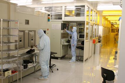
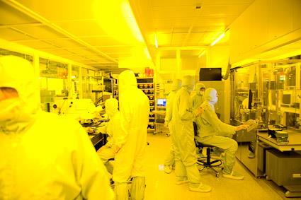
2 Delft University of Technology Delft Institute of Microsystems and Nanoelectronics Class 100, 100 mm wafer size Full IC & MEMS processing line 2
3 Overview Graphene Properties Applications: chemical and Hall sensors Approaches of graphene manufacturing Towards wafer-scale fabrication Graphene layer transfer Integration aspects Conclusion 3

 First 2D material 4")
4 Graphene Single atom layer of graphite Theoretically known since 1947 First isolated in 2004 by Geim and Novoselov (Noble price 2010) First 2D material 4
5 Graphene properties Single-atom thickness: 0.34 nm Strongest material (> 1 Tpa), while extremely flexible Stainless steel 200 GPa Huge electron mobility (theoretically 200,000 cm K) Silicon 1400 cm 2 /Vs Optically transparent (2.3% absorption per layer) High thermal conductivity (>4800 W/mK) Copper 400 W/mK 2D: only surface, no bulk: extremely sensitive to interaction with surroundings Planar technology 5


")
6 Potential applications Field effect transistors Chemical sensors Hall sensors (magnetic field) Supercapacitors Interconnects Transparant electrodes Flexible electronics Thermal management Quantum dots Nanopores (DNA sequencing) Resistance standard 6

7 Graphene FET High mobility No bandgap! Bandgap engineering possible Nano-ribbons Bi-layer graphene Resulting bandgap low Worse: reduces mobility Other new 2D materials have intrinsic bandgap (e.g. MoS 2 ) Y.-M. Lin et al, Sciene vol. 327 p. 662 (2010) 7

8 Graphene for chemical sensors No bulk: sensitivity Low noise Adsorption of molecules onto surface changes resistance, or FET transfer characteristics Possible to detect single molecules Can be functionalized F. Schedin et al. Nature 6, p. 652 (2007) 8
 High mobility Large Hall sensitivity Thin material Low noise Simple")
9 Graphene for Hall sensors Xu et al. Scientific Reports 3, 1207 (2013) High mobility Large Hall sensitivity Thin material Low noise Simple design Highly linear 1500 V/AT sensitivity demonstrated (Si 100 V/AT) 9
10 Graphene market predictions (transparent conductive films) March,

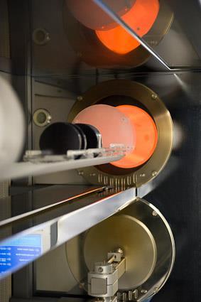
11 Graphene fabrication 11

12 Industrial up scaling? 12


13 Alternatives? Exfoliation using tape Exfoliation using ultrasonic Highest quality, flakes Never fit for industry SiC: ablation High quality, suspension Not suitable for wafer fabrication Chemical vapour deposition (CVD) 13

 No 8 or 12 substrates")
14 Epitaxial growth from SiC By heating up crystalline (4H or 6H) SiC to ~1500 C in high vacuum Si ablates, leaving C Large area (cm 2 ) High quality On top of semiconductor layer Extremely expensive substrate (2 wafer: ~$ 1000) No 8 or 12 substrates available? 14


15 Chemical vapour deposition Mono-layer: Cu Multi-layer: Ni, Co 15


 2 n B ~ e L Vgate Magnetic field (T)")

16 Back gate voltage (V) High quality CVD graphene Group at TU Delft demonstrated CVD graphene on Cu films with 1 µm ballistic conduction at 4K by transverse magnetic focusing Mobility up to 20,000 cm K, mm-size graphene flakes (in press) 2 n B ~ e L Vgate Magnetic field (T) V/I bias (kω) Shou-En Zhu, Victor Calado, Lieven Vandersypen, Guido Janssen. Graphene 2013, Bilbao, Spain 16


17 Direct growth on wafers Scalability of thin metal foils to > 4 wafer size poor Direct growth on wafers required: catalyst on oxidized wafer First 300 mm tool installed in AIST, Japan 17
 Difficult to see graphene, spectroscopy techniques")
18 Analysing graphene 3.5 2D 3.0 Normalized intensity (a.u.) D G Raman shift (cm -1 ) Difficult to see graphene, spectroscopy techniques required 18

19 Transfer process Growth on wafers is scaling up fast However, layer still has to be transferred 19

20 Transfer results Wafer scale transfer still problematic Mobility low, although material is of good quality: polymer residues after transfer Tao et al. J. Phys. Chem. C 116, (2012) 20
21 Alternative transfer methods? Circumvent use of polymer? Etching away Cu to release graphene problematic for large wafers No etching: peal-off graphene film by promoting adhesion to target? Demonstrated for multi-layer graphene using PDMS Wafer-to-wafer direct transfer? Graphene layer transfer biggest challenge in graphene wafer-scale manufacturing 21
 Graphene integration Graphene likely first a back-end material Contamination issues Low resistance contact formation Au Ti Layer quality after transfer is key For Hall sensors & transistors")
22 Watanabe et al, Diam. Relat. Mater. 24 (2012) Graphene integration Graphene likely first a back-end material Contamination issues Low resistance contact formation Au Ti Layer quality after transfer is key For Hall sensors & transistors high mobility required For chemical sensors quality demands less strict (but need functionalization) Most demonstrators single-shot devices: manufacturability hardly investigated. 22
23 Graphene: the next carbon nanotubes? After 20+ years or research on carbon nanotubes (CNT) still hardly any commercial application Properties of CNT very similar to graphene Fabrication issues holding back application of CNT: overhyped? Could the same happen to graphene? Advantage graphene: planar Investigation of manufacturability and scalability Use graphene where it has the advantage: sensors, transparent electrodes, flexible electronics, etc. Graphene FET? Maybe another 2D material will do better (MoS 2 ) 23
24 Conclusion Graphene is attractive material for sensors, transparent and flexible electronics Industrial production material holding back implementation CVD graphene most attractive method Scalable to 30 cm wafers Quality as good as exfoliated graphene Wafer transfer key: no transfer no practical use Manufacturability and uniformity have to be studied in detail 24
Graphene films on silicon carbide (SiC) wafers supplied by Nitride Crystals, Inc.
 wafers supplied by Nitride Crystals, Inc.") 9702 Gayton Road, Suite 320, Richmond, VA 23238, USA Phone: +1 (804) 709-6696 info@nitride-crystals.com www.nitride-crystals.com Graphene films on silicon carbide (SiC) wafers supplied by Nitride Crystals,
9702 Gayton Road, Suite 320, Richmond, VA 23238, USA Phone: +1 (804) 709-6696 info@nitride-crystals.com www.nitride-crystals.com Graphene films on silicon carbide (SiC) wafers supplied by Nitride Crystals,
Overview. Carbon in all its forms. Background & Discovery Fabrication. Important properties. Summary & References. Overview of current research
 Graphene Prepared for Solid State Physics II Pr Dagotto Spring 2009 Laurene Tetard 03/23/09 Overview Carbon in all its forms Background & Discovery Fabrication Important properties Overview of current
A. Optimizing the growth conditions of large-scale graphene films
 1 A. Optimizing the growth conditions of large-scale graphene films Figure S1. Optical microscope images of graphene films transferred on 300 nm SiO 2 /Si substrates. a, Images of the graphene films grown
Scaling up Chemical Vapor Deposition Graphene to 300 mm Si substrates
 Scaling up Chemical Vapor Deposition Graphene to 300 mm Si substrates Co- Authors Aixtron Alex Jouvray Simon Buttress Gavin Dodge Ken Teo The work shown here has received partial funding from the European
Graphene Novel Material for Nanoelectronics
 Graphene Novel Material for Nanoelectronics Shintaro Sato Naoki Harada Daiyu Kondo Mari Ohfuchi (Manuscript received May 12, 2009) Graphene is a flat monolayer of carbon atoms with a two-dimensional honeycomb
Graphene. Tianyu Ye November 30th, 2011
 Graphene Tianyu Ye November 30th, 2011 Outline What is graphene? How to make graphene? (Exfoliation, Epitaxial, CVD) Is it graphene? (Identification methods) Transport properties; Other properties; Applications;
CVD growth of Graphene. SPE ACCE presentation Carter Kittrell James M. Tour group September 9 to 11, 2014
 CVD growth of Graphene SPE ACCE presentation Carter Kittrell James M. Tour group September 9 to 11, 2014 Graphene zigzag armchair History 1500: Pencil-Is it made of lead? 1789: Graphite 1987: The first
Nanostrukturphysik (Nanostructure Physics)
") Nanostrukturphysik (Nanostructure Physics) Prof. Yong Lei & Dr. Yang Xu Fachgebiet 3D-Nanostrukturierung, Institut für Physik Contact: yong.lei@tu-ilmenau.de; yang.xu@tu-ilmenau.de Office: Unterpoerlitzer
Nanostrukturphysik (Nanostructure Physics) Prof. Yong Lei & Dr. Yang Xu Fachgebiet 3D-Nanostrukturierung, Institut für Physik Contact: yong.lei@tu-ilmenau.de; yang.xu@tu-ilmenau.de Office: Unterpoerlitzer
Carbon Nanomaterials: Nanotubes and Nanobuds and Graphene towards new products 2030
 Carbon Nanomaterials: Nanotubes and Nanobuds and Graphene towards new products 2030 Prof. Dr. Esko I. Kauppinen Helsinki University of Technology (TKK) Espoo, Finland Forecast Seminar February 13, 2009
Graphene Fundamentals and Emergent Applications
 Graphene Fundamentals and Emergent Applications Jamie H. Warner Department of Materials University of Oxford Oxford, UK Franziska Schaffel Department of Materials University of Oxford Oxford, UK Alicja
Session V: Graphene. Matteo Bruna CAMBRIDGE UNIVERSITY DEPARTMENT OF ENGINEERING
 Session V: Graphene Matteo Bruna Graphene: Material in the Flatland Graphite Graphene Properties: Thinnest imaginable material Good(and tunable) electrical conductor Strongest ever measured Stiffest known
Graphene devices and integration: A primer on challenges
 Graphene devices and integration: A primer on challenges Archana Venugopal (TI) 8 Nov 2016 Acknowledgments: Luigi Colombo (TI) UT Dallas and UT Austin 1 Outline Where we are Issues o Contact resistance
Supplementary Figure 1: Micromechanical cleavage of graphene on oxygen plasma treated Si/SiO2. Supplementary Figure 2: Comparison of hbn yield.
 1 2 3 4 Supplementary Figure 1: Micromechanical cleavage of graphene on oxygen plasma treated Si/SiO 2. Optical microscopy images of three examples of large single layer graphene flakes cleaved on a single
Exceptional ballistic transport in epigraphene. Walt de Heer Georgia Institute of Technology
 Exceptional ballistic transport in epigraphene Walt de Heer Georgia Institute of Technology Program Objective First formulated in 2001 and patented in 2003, our objective is to develop nanoelectronics
Supplementary Figure S1. AFM images of GraNRs grown with standard growth process. Each of these pictures show GraNRs prepared independently,
 Supplementary Figure S1. AFM images of GraNRs grown with standard growth process. Each of these pictures show GraNRs prepared independently, suggesting that the results is reproducible. Supplementary Figure
Initial Stages of Growth of Organic Semiconductors on Graphene
 Initial Stages of Growth of Organic Semiconductors on Graphene Presented by: Manisha Chhikara Supervisor: Prof. Dr. Gvido Bratina University of Nova Gorica Outline Introduction to Graphene Fabrication
Nanotechnology in Consumer Products
 Nanotechnology in Consumer Products June 17, 2015 October 31, 2014 The webinar will begin at 1pm Eastern Time Perform an audio check by going to Tools > Audio > Audio Setup Wizard Chat Box Chat Box Send
TRANSVERSE SPIN TRANSPORT IN GRAPHENE
 International Journal of Modern Physics B Vol. 23, Nos. 12 & 13 (2009) 2641 2646 World Scientific Publishing Company TRANSVERSE SPIN TRANSPORT IN GRAPHENE TARIQ M. G. MOHIUDDIN, A. A. ZHUKOV, D. C. ELIAS,
SUPPLEMENTARY INFORMATION
 SUPPLEMENTARY INFORMATION Facile Synthesis of High Quality Graphene Nanoribbons Liying Jiao, Xinran Wang, Georgi Diankov, Hailiang Wang & Hongjie Dai* Supplementary Information 1. Photograph of graphene
Nanostrukturphysik Übung 2 (Class 3&4)
") Nanostrukturphysik Übung 2 (Class 3&4) Prof. Yong Lei & Dr. Yang Xu 2017.05.03 Fachgebiet 3D-Nanostrukturierung, Institut für Physik Contact: yong.lei@tu-ilmenau.de (3748), yang.xu@tuilmenau.de (4902)
Nanostrukturphysik Übung 2 (Class 3&4) Prof. Yong Lei & Dr. Yang Xu 2017.05.03 Fachgebiet 3D-Nanostrukturierung, Institut für Physik Contact: yong.lei@tu-ilmenau.de (3748), yang.xu@tuilmenau.de (4902)
Supplementary Figure 1 Experimental setup for crystal growth. Schematic drawing of the experimental setup for C 8 -BTBT crystal growth.
 Supplementary Figure 1 Experimental setup for crystal growth. Schematic drawing of the experimental setup for C 8 -BTBT crystal growth. Supplementary Figure 2 AFM study of the C 8 -BTBT crystal growth
EN2912C: Future Directions in Computing Lecture 08: Overview of Near-Term Emerging Computing Technologies
 EN2912C: Future Directions in Computing Lecture 08: Overview of Near-Term Emerging Computing Technologies Prof. Sherief Reda Division of Engineering Brown University Fall 2008 1 Near-term emerging computing
Graphene FETs EE439 FINAL PROJECT. Yiwen Meng Su Ai
 Graphene FETs EE439 FINAL PROJECT Yiwen Meng Su Ai Introduction What is Graphene? An atomic-scale honeycomb lattice made of carbon atoms Before 2004, Hypothetical Carbon Structure Until 2004, physicists
Supplementary Information for
 Supplementary Information for Highly Stable, Dual-Gated MoS 2 Transistors Encapsulated by Hexagonal Boron Nitride with Gate-Controllable Contact Resistance and Threshold Voltage Gwan-Hyoung Lee, Xu Cui,
Transparent Electrode Applications
 Transparent Electrode Applications LCD Solar Cells Touch Screen Indium Tin Oxide (ITO) Zinc Oxide (ZnO) - High conductivity - High transparency - Resistant to environmental effects - Rare material (Indium)
Conference Return Seminar- NANO2014,Moscow State University,Moscow,Russia Date: th July 2014
 Conference Return Seminar- NANO2014,Moscow State University,Moscow,Russia Date:13-1818 th July 2014 An electrochemical method for the synthesis of single and few layers graphene sheets for high temperature
A BIT OF MATERIALS SCIENCE THEN PHYSICS
 GRAPHENE AND OTHER D ATOMIC CRYSTALS Andre Geim with many thanks to K. Novoselov, S. Morozov, D. Jiang, F. Schedin, I. Grigorieva, J. Meyer, M. Katsnelson A BIT OF MATERIALS SCIENCE THEN PHYSICS CARBON
Carbon Nanotubes in Interconnect Applications
 Carbon Nanotubes in Interconnect Applications Page 1 What are Carbon Nanotubes? What are they good for? Why are we interested in them? - Interconnects of the future? Comparison of electrical properties
.Fritjaf Capra, The Tao of Physics
 Probing inside the atom and investigating its structure, science transcended the limits of our sensory imagination. From this point on, it could no longer rely with absolute certainty on logic and common
Intrinsic Electronic Transport Properties of High. Information
 Intrinsic Electronic Transport Properties of High Quality and MoS 2 : Supporting Information Britton W. H. Baugher, Hugh O. H. Churchill, Yafang Yang, and Pablo Jarillo-Herrero Department of Physics, Massachusetts
Supporting Information Available:
 Supporting Information Available: Photoresponsive and Gas Sensing Field-Effect Transistors based on Multilayer WS 2 Nanoflakes Nengjie Huo 1, Shengxue Yang 1, Zhongming Wei 2, Shu-Shen Li 1, Jian-Bai Xia
Supporting Online Material for
 www.sciencemag.org/cgi/content/full/327/5966/662/dc Supporting Online Material for 00-GHz Transistors from Wafer-Scale Epitaxial Graphene Y.-M. Lin,* C. Dimitrakopoulos, K. A. Jenkins, D. B. Farmer, H.-Y.
Grpahene Synthesis by CVD. QingkaiYu Ingram School of Engineering Texas State University at San Marcos
 Grpahene Synthesis by CVD QingkaiYu Ingram School of Engineering Texas State University at San Marcos @ Applied Nanotech Inc, July 25 th, 2011 Acknowledgement Texas State University Dr. Zhihong Liu Austin
Carbon based Nanoscale Electronics
 Carbon based Nanoscale Electronics 09 02 200802 2008 ME class Outline driving force for the carbon nanomaterial electronic properties of fullerene exploration of electronic carbon nanotube gold rush of
Carbon Nanotubes for Interconnect Applications Franz Kreupl, Andrew P. Graham, Maik Liebau, Georg S. Duesberg, Robert Seidel, Eugen Unger
 Carbon Nanotubes for Interconnect Applications Franz Kreupl, Andrew P. Graham, Maik Liebau, Georg S. Duesberg, Robert Seidel, Eugen Unger Infineon Technologies Corporate Research Munich, Germany Outline
Supporting Information. Fast Synthesis of High-Performance Graphene by Rapid Thermal Chemical Vapor Deposition
 1 Supporting Information Fast Synthesis of High-Performance Graphene by Rapid Thermal Chemical Vapor Deposition Jaechul Ryu, 1,2, Youngsoo Kim, 4, Dongkwan Won, 1 Nayoung Kim, 1 Jin Sung Park, 1 Eun-Kyu
1. Nanotechnology & nanomaterials -- Functional nanomaterials enabled by nanotechnologies.
 Novel Nano-Engineered Semiconductors for Possible Photon Sources and Detectors NAI-CHANG YEH Department of Physics, California Institute of Technology 1. Nanotechnology & nanomaterials -- Functional nanomaterials
There's Plenty of Room at the Bottom
 There's Plenty of Room at the Bottom 12/29/1959 Feynman asked why not put the entire Encyclopedia Britannica (24 volumes) on a pin head (requires atomic scale recording). He proposed to use electron microscope
Application of Graphene to High-Speed Transistors: Expectations and Challenges
 5 Application of Graphene to High-Speed Transistors: Expectations and Challenges Yasushi IYECHIKA Nanotechnology and Materials Unit 1 Introduction 1-1 Discovery of Graphene; Potentiality of Breaking through
What are Carbon Nanotubes? What are they good for? Why are we interested in them?
 Growth and Properties of Multiwalled Carbon Nanotubes What are Carbon Nanotubes? What are they good for? Why are we interested in them? - Interconnects of the future? - our vision Where do we stand - our
The Low Temperature Physics of Thin Films Superconducting Tin and Monolayer Graphene
 The Low Temperature Physics of Thin Films Superconducting Tin and Monolayer Graphene Abstract: The aim of this project was to investigate how the electrical resistance of a conductor changes if it is deposited
Workshop II Nanomaterials Surfaces and Layers Commercialising Carbon Nanotubes
 Workshop II Nanomaterials Surfaces and Layers Commercialising Carbon Nanotubes Harry Swan, Carbon Nanomaterials Business Manager, Thomas Swan & Co. Ltd. Introduction Thomas Swan & Co. Ltd. Carbon Nanotubes
Commercial Graphene Applications: Current Research and Future Prospects
 Commercial Graphene Applications: Current Research and Future Prospects Overview History and Overview of Graphene Angstron Materials and Nanotek Instruments Applications of Graphene Thermal Management
2D Materials for Gas Sensing
 2D Materials for Gas Sensing S. Guo, A. Rani, and M.E. Zaghloul Department of Electrical and Computer Engineering The George Washington University, Washington DC 20052 Outline Background Structures of
Supplementary Figure 1 Dark-field optical images of as prepared PMMA-assisted transferred CVD graphene films on silicon substrates (a) and the one
 and the one") Supplementary Figure 1 Dark-field optical images of as prepared PMMA-assisted transferred CVD graphene films on silicon substrates (a) and the one after PBASE monolayer growth (b). 1 Supplementary Figure
Supplementary Figure 1 Dark-field optical images of as prepared PMMA-assisted transferred CVD graphene films on silicon substrates (a) and the one after PBASE monolayer growth (b). 1 Supplementary Figure
Graphene Transfer and Characterization
 Macalester Journal of Physics and Astronomy Volume 1 Issue 1 Spring 2013 Article 8 May 2013 Graphene Transfer and Characterization Rolan Manderson-Jones Macalester College, rbmandersonjones@gmail.com Abstract
SUPPLEMENTARY INFORMATION
 SUPPLEMENTARY INFORMATION Flexible, high-performance carbon nanotube integrated circuits Dong-ming Sun, Marina Y. Timmermans, Ying Tian, Albert G. Nasibulin, Esko I. Kauppinen, Shigeru Kishimoto, Takashi
Nanocarbon Technology for Development of Innovative Devices
 Nanocarbon Technology for Development of Innovative Devices Shintaro Sato Daiyu Kondo Shinichi Hirose Junichi Yamaguchi Graphene, a one-atom-thick honeycomb lattice made of carbon, and a carbon nanotube,
Optimizing Graphene Morphology on SiC(0001)
") Optimizing Graphene Morphology on SiC(0001) James B. Hannon Rudolf M. Tromp Graphene sheets Graphene sheets can be formed into 0D,1D, 2D, and 3D structures Chemically inert Intrinsically high carrier mobility
Optimizing Graphene Morphology on SiC(0001) James B. Hannon Rudolf M. Tromp Graphene sheets Graphene sheets can be formed into 0D,1D, 2D, and 3D structures Chemically inert Intrinsically high carrier mobility
Graphene: Plane and Simple Electrical Metrology?
 Graphene: Plane and Simple Electrical Metrology? R. E. Elmquist, F. L. Hernandez-Marquez, M. Real, T. Shen, D. B. Newell, C. J. Jacob, and G. R. Jones, Jr. National Institute of Standards and Technology,
SUPPLEMENTARY INFORMATION
 Hihly efficient ate-tunable photocurrent eneration in vertical heterostructures of layered materials Woo Jon Yu, Yuan Liu, Hailon Zhou, Anxian Yin, Zhen Li, Yu Huan, and Xianfen Duan. Schematic illustration
Figure 1: Graphene release, transfer and stacking processes. The graphene stacking began with CVD
 Supplementary figure 1 Graphene Growth and Transfer Graphene PMMA FeCl 3 DI water Copper foil CVD growth Back side etch PMMA coating Copper etch in 0.25M FeCl 3 DI water rinse 1 st transfer DI water 1:10
Transient Photocurrent Measurements of Graphene Related Materials
 Transient Photocurrent Measurements of Graphene Related Materials P. Srinivasa Rao Mentor: Prof. dr. Gvido Bratina Laboratory of Organic Matter Physics University of Nova Gorica 1 Contents: 1. Electrical
vapour deposition. Raman peaks of the monolayer sample grown by chemical vapour
 Supplementary Figure 1 Raman spectrum of monolayer MoS 2 grown by chemical vapour deposition. Raman peaks of the monolayer sample grown by chemical vapour deposition (S-CVD) are peak which is at 385 cm
SUPPLEMENTARY INFORMATION. Observation of tunable electrical bandgap in large-area twisted bilayer graphene synthesized by chemical vapor deposition
 SUPPLEMENTARY INFORMATION Observation of tunable electrical bandgap in large-area twisted bilayer graphene synthesized by chemical vapor deposition Jing-Bo Liu 1 *, Ping-Jian Li 1 *, Yuan-Fu Chen 1, Ze-Gao
Nanostrukturphysik (Nanostructure Physics)
") Nanostrukturphysik (Nanostructure Physics) Prof. Yong Lei & Dr. Yang Xu Fachgebiet 3D-Nanostrukturierung, Institut für Physik Contact: yong.lei@tu-ilmenau.de; yang.xu@tu-ilmenau.de Office: Unterpoerlitzer
Nanostrukturphysik (Nanostructure Physics) Prof. Yong Lei & Dr. Yang Xu Fachgebiet 3D-Nanostrukturierung, Institut für Physik Contact: yong.lei@tu-ilmenau.de; yang.xu@tu-ilmenau.de Office: Unterpoerlitzer
30-Inch Roll-Based Production of High-Quality Graphene Films for Flexible Transparent Electrodes
 30-Inch Roll-Based Production of High-Quality Graphene Films for Flexible Transparent Electrodes Sukang Bae, 1* Hyeong Keun Kim, 3* Xianfang Xu, 5 Jayakumar Balakrishnan, 5 Tian Lei, 1 Young Il Song, 6
Emerging Research Devices: A Study of CNTFET and SET as a replacement for SiMOSFET
 1 Emerging Research Devices: A Study of CNTFET and SET as a replacement for SiMOSFET Mahmoud Lababidi, Krishna Natarajan, Guangyu Sun Abstract Since the development of the Silicon MOSFET, it has been the
Nanoelectronics. Topics
 Nanoelectronics Topics Moore s Law Inorganic nanoelectronic devices Resonant tunneling Quantum dots Single electron transistors Motivation for molecular electronics The review article Overview of Nanoelectronic
Supporting information
 Supporting information Influence of electrolyte composition on liquid-gated carbon-nanotube and graphene transistors By: Iddo Heller, Sohail Chatoor, Jaan Männik, Marcel A. G. Zevenbergen, Cees Dekker,
NiCl2 Solution concentration. Etching Duration. Aspect ratio. Experiment Atmosphere Temperature. Length(µm) Width (nm) Ar:H2=9:1, 150Pa
 Width (nm) Ar:H2=9:1, 150Pa") Experiment Atmosphere Temperature #1 # 2 # 3 # 4 # 5 # 6 # 7 # 8 # 9 # 10 Ar:H2=9:1, 150Pa Ar:H2=9:1, 150Pa Ar:H2=9:1, 150Pa Ar:H2=9:1, 150Pa Ar:H2=9:1, 150Pa Ar:H2=9:1, 150Pa Ar:H2=9:1, 150Pa Ar:H2=9:1,
Experiment Atmosphere Temperature #1 # 2 # 3 # 4 # 5 # 6 # 7 # 8 # 9 # 10 Ar:H2=9:1, 150Pa Ar:H2=9:1, 150Pa Ar:H2=9:1, 150Pa Ar:H2=9:1, 150Pa Ar:H2=9:1, 150Pa Ar:H2=9:1, 150Pa Ar:H2=9:1, 150Pa Ar:H2=9:1,
SiC Graphene Suitable For Quantum Hall Resistance Metrology.
 SiC Graphene Suitable For Quantum Hall Resistance Metrology. Samuel Lara-Avila 1, Alexei Kalaboukhov 1, Sara Paolillo, Mikael Syväjärvi 3, Rositza Yakimova 3, Vladimir Fal'ko 4, Alexander Tzalenchuk 5,
Recap (so far) Low-Dimensional & Boundary Effects
 Low-Dimensional & Boundary Effects") Recap (so far) Ohm s & Fourier s Laws Mobility & Thermal Conductivity Heat Capacity Wiedemann-Franz Relationship Size Effects and Breakdown of Classical Laws 1 Low-Dimensional & Boundary Effects Energy
Recap (so far) Ohm s & Fourier s Laws Mobility & Thermal Conductivity Heat Capacity Wiedemann-Franz Relationship Size Effects and Breakdown of Classical Laws 1 Low-Dimensional & Boundary Effects Energy
Nanostructures. Lecture 13 OUTLINE
 Nanostructures MTX9100 Nanomaterials Lecture 13 OUTLINE -What is quantum confinement? - How can zero-dimensional materials be used? -What are one dimensional structures? -Why does graphene attract so much
2D MBE Activities in Sheffield. I. Farrer, J. Heffernan Electronic and Electrical Engineering The University of Sheffield
 2D MBE Activities in Sheffield I. Farrer, J. Heffernan Electronic and Electrical Engineering The University of Sheffield Outline Motivation Van der Waals crystals The Transition Metal Di-Chalcogenides
Carbon Nanotube Thin-Films & Nanoparticle Assembly
 Nanodevices using Nanomaterials : Carbon Nanotube Thin-Films & Nanoparticle Assembly Seung-Beck Lee Division of Electronics and Computer Engineering & Department of Nanotechnology, Hanyang University,
Wafer Scale Homogeneous Bilayer Graphene Films by. Chemical Vapor Deposition
 Supporting Information for Wafer Scale Homogeneous Bilayer Graphene Films by Chemical Vapor Deposition Seunghyun Lee, Kyunghoon Lee, Zhaohui Zhong Department of Electrical Engineering and Computer Science,
Graphene based FETs. Raghav Gupta ( )
") 1 Graphene based FETs Raghav Gupta (10327553) Abstract The extraordinary electronic properties along with excellent optical, mechanical, thermodynamic properties have led to a lot of interest in its possible
1 Graphene based FETs Raghav Gupta (10327553) Abstract The extraordinary electronic properties along with excellent optical, mechanical, thermodynamic properties have led to a lot of interest in its possible
Graphene and Carbon Nanotubes
 Graphene and Carbon Nanotubes 1 atom thick films of graphite atomic chicken wire Novoselov et al - Science 306, 666 (004) 100μm Geim s group at Manchester Novoselov et al - Nature 438, 197 (005) Kim-Stormer
ConceptGraphene. Small or medium-scale focused research project. WP1 Fabrication
 ConceptGraphene New Electronics Concept: Wafer-Scale Epitaxial Graphene Small or medium-scale focused research project WP1 Fabrication Deliverable 1.2 Quality comparison: epitaxial graphene vs graphene
2011 GCEP Report. Project title: Self-sorting of Carbon Nanotubes for High Performance Large Area Transparent Electrodes for Solar Cells
 2011 GCEP Report Project title: Self-sorting of Carbon Nanotubes for High Performance Large Area Transparent Electrodes for Solar Cells Investigators Zhenan Bao, Associate Professor, Chemical Engineering
Graphene Canada Montreal Oct. 16, 2015 (International Year of Light)
") Luminescence Properties of Graphene A. Beltaos 1,2,3, A. Bergren 1, K. Bosnick 1, N. Pekas 1, A. Matković 4, A. Meldrum 2 1 National Institute for Nanotechnology (NINT), 11421 Saskatchewan Drive, Edmonton,
Luminescence Properties of Graphene A. Beltaos 1,2,3, A. Bergren 1, K. Bosnick 1, N. Pekas 1, A. Matković 4, A. Meldrum 2 1 National Institute for Nanotechnology (NINT), 11421 Saskatchewan Drive, Edmonton,
Fermi Level Pinning at Electrical Metal Contacts. of Monolayer Molybdenum Dichalcogenides
 Supporting information Fermi Level Pinning at Electrical Metal Contacts of Monolayer Molybdenum Dichalcogenides Changsik Kim 1,, Inyong Moon 1,, Daeyeong Lee 1, Min Sup Choi 1, Faisal Ahmed 1,2, Seunggeol
XPS Depth Profiling of Epitaxial Graphene Intercalated with FeCl 3
 XPS Depth Profiling of Epitaxial Graphene Intercalated with FeCl 3 Mahdi Ibrahim Maynard H. Jackson High School Atlanta, GA. Faculty Advisor: Dr. Kristin Shepperd Research Group: Prof. Edward Conrad School
Engineered Flexible Conductive Barrier Films for Advanced Energy Devices
 The 13 th Korea-U.S. Forum on Nanotechnology Engineered Flexible Conductive Barrier Films for Advanced Energy Devices Jinsung Kwak 1, Yongsu Jo 1, Soon-Dong Park 2, Na Yeon Kim 1, Se-Yang Kim 1, Zonghoon
2D-2D tunneling field effect transistors using
 2D-2D tunneling field effect transistors using WSe 2 /SnSe 2 heterostructures Tania Roy, 1,2,3 Mahmut Tosun, 1,2,3 Mark Hettick, 1,2,3, Geun Ho Ahn, 1,2,3 Chenming Hu 1, and Ali Javey 1,2,3, 1 Electrical
Graphene-reinforced elastomers for demanding environments
 Graphene-reinforced elastomers for demanding environments Robert J Young, Ian A. Kinloch, Dimitrios G. Papageorgiou, J. Robert Innes and Suhao Li School of Materials and National Graphene Institute The
Solutions for Assignment-8
 Solutions for Assignment-8 Q1. The process of adding impurities to a pure semiconductor is called: [1] (a) Mixing (b) Doping (c) Diffusing (d) None of the above In semiconductor production, doping intentionally
STM and graphene. W. W. Larry Pai ( 白偉武 ) Center for condensed matter sciences, National Taiwan University NTHU, 2013/05/23
 Center for condensed matter sciences, National Taiwan University NTHU, 2013/05/23") STM and graphene W. W. Larry Pai ( 白偉武 ) Center for condensed matter sciences, National Taiwan University NTHU, 2013/05/23 Why graphene is important: It is a new form of material (two dimensional, single
STM and graphene W. W. Larry Pai ( 白偉武 ) Center for condensed matter sciences, National Taiwan University NTHU, 2013/05/23 Why graphene is important: It is a new form of material (two dimensional, single
Beyond silicon electronics-fets with nanostructured graphene channels with high on-off ratio and highmobility
 Beyond silicon electronics-fets with nanostructured graphene channels with high on-off ratio and highmobility M.Dragoman 1, A.Dinescu 1, and D.Dragoman 2 1 National Institute for Research and Development
Graphene Process and Device Options for Microelectronics Applications
 Graphene Process and Device Options for Microelectronics Applications Max Lemme KTH Royal Institute of Technology School of Information and Communication Technology lemme@kth.se 31 May 2012 Graphene Process
Multicolor Graphene Nanoribbon/Semiconductor Nanowire. Heterojunction Light-Emitting Diodes
 Multicolor Graphene Nanoribbon/Semiconductor Nanowire Heterojunction Light-Emitting Diodes Yu Ye, a Lin Gan, b Lun Dai, *a Hu Meng, a Feng Wei, a Yu Dai, a Zujin Shi, b Bin Yu, a Xuefeng Guo, b and Guogang
Plastic Electronics. Joaquim Puigdollers.
 Plastic Electronics Joaquim Puigdollers Joaquim.puigdollers@upc.edu Nobel Prize Chemistry 2000 Origins Technological Interest First products.. MONOCROMATIC PHILIPS Today Future Technological interest Low
Chemical Vapour Deposition of Large-area High-quality Graphene Films for Electronic Applications
 Chemical Vapour Deposition of Large-area High-quality Graphene Films for Electronic Applications Kai WANG A thesis submitted to Imperial College London In fulfilment of the requirements for the degree
Graphene conductivity mapping by terahertz time-domain reflection spectroscopy
 Graphene conductivity mapping by terahertz time-domain reflection spectroscopy Xiaodong Feng, Min Hu *, Jun Zhou, and Shenggang Liu University of Electronic Science and Technology of China Terahertz Science
Ph.D. students, postdocs, and young researchers, which need to absorb a lot of new knowledge, not taught at universities, in a rather short time.
 We have started to work in the area of graphene at the end of 2006, discovering that the fascinating Dirac equations could drive to new discoveries in solid-state physics. At that time, although the Dirac
Efficient Preparation of Large-Area Graphene Oxide Sheets for Transparent Conductive Films
 Supporting Information Efficient Preparation of Large-Area Graphene Oxide Sheets for Transparent Conductive Films Jinping Zhao, Songfeng Pei, Wencai Ren*, Libo Gao and Hui-Ming Cheng* Shenyang National
Investigation Report of Graphene
 Investigation Report of Graphene Reporter: Shao Xiaoru Superviser: Prof.Zhao & Dr. Hong 2014-4-14 Contents 1 Basic Knowledge 2 Synthesis Method 3 Research Progress 4 Future research directions 2 Omnipotent
NEM Relays Using 2-Dimensional Nanomaterials for Low Energy Contacts
 NEM Relays Using 2-Dimensional Nanomaterials for Low Energy Contacts Seunghyun Lee, Ji Cao 10/29/2013 A Science & Technology Professor H. -S. Philip Wong Electrical Engineering, Stanford University Center
SUPPLEMENTARY INFORMATION
 doi:.38/nature09979 I. Graphene material growth and transistor fabrication Top-gated graphene RF transistors were fabricated based on chemical vapor deposition (CVD) grown graphene on copper (Cu). Cu foil
Low Voltage Field Emission SEM (LV FE-SEM): A Promising Imaging Approach for Graphene Samples
: A Promising Imaging Approach for Graphene Samples") Low Voltage Field Emission SEM (LV FE-SEM): A Promising Imaging Approach for Graphene Samples Jining Xie Agilent Technologies May 23 rd, 2012 www.agilent.com/find/nano Outline 1. Introduction 2. Agilent
Low Voltage Field Emission SEM (LV FE-SEM): A Promising Imaging Approach for Graphene Samples Jining Xie Agilent Technologies May 23 rd, 2012 www.agilent.com/find/nano Outline 1. Introduction 2. Agilent
Introduction to Nanotechnology Chapter 5 Carbon Nanostructures Lecture 1
 Introduction to Nanotechnology Chapter 5 Carbon Nanostructures Lecture 1 ChiiDong Chen Institute of Physics, Academia Sinica chiidong@phys.sinica.edu.tw 02 27896766 Carbon contains 6 electrons: (1s) 2,
GRAPHENE the first 2D crystal lattice
 GRAPHENE the first 2D crystal lattice dimensionality of carbon diamond, graphite GRAPHENE realized in 2004 (Novoselov, Science 306, 2004) carbon nanotubes fullerenes, buckyballs what s so special about
DEPOSITION OF THIN TiO 2 FILMS BY DC MAGNETRON SPUTTERING METHOD
 Chapter 4 DEPOSITION OF THIN TiO 2 FILMS BY DC MAGNETRON SPUTTERING METHOD 4.1 INTRODUCTION Sputter deposition process is another old technique being used in modern semiconductor industries. Sputtering
Evolution of graphene growth on Cu and Ni studied by carbon isotope
 Evolution of graphene growth on Cu and Ni studied by carbon isotope labeling Xuesong Li a, Weiwei Cai a, Luigi Colombo b*, and Rodney S. Ruoff a* Large-area graphene is a new material with properties that
Cut-and-Paste Organic FET Customized ICs for Application to Artificial Skin
 Cut-and-Paste Organic FET Customized ICs for Application to Artificial Skin Takao Someya 1, Hiroshi Kawaguchi 2, Takayasu Sakurai 3 1 School of Engineering, University of Tokyo, Tokyo, JAPAN 2 Institute
Supplementary Figures
 Supplementary Figures 1500 Heating Annealing Growing Cooling 20 Temperature ( o C) 1000 500 Ar:H 2 = 5:1 Ar:H 2 = 5:1 15 10 5 Pressure(Pa) 0 Ar(SiH 4 (5%)):C 2 H 2 = 1:2 120 mins 5 mins 5 40 mins ~120
Impact of intrinsic deformations on the negative differential resistance of monolayer MoS 2 ultrashort channel MOSFET
 Impact of intrinsic deformations on the negative differential resistance of monolayer MoS 2 ultrashort channel MOSFET Amretashis Sengupta*, Santanu Mahapatra Nano-Scale Device Research Laboratory, Dept.
Supporting Information for: Electrical probing and tuning of molecular. physisorption on graphene
 Supporting Information for: Electrical probing and tuning of molecular physisorption on graphene Girish S. Kulkarni, Karthik Reddy #, Wenzhe Zang, Kyunghoon Lee, Xudong Fan *, and Zhaohui Zhong * Department
SUPPLEMENTARY INFORMATION
 SUPPLEMENTARY INFORMATION SUPPLEMENTARY INFORMATION Trilayer graphene is a semimetal with a gate-tuneable band overlap M. F. Craciun, S. Russo, M. Yamamoto, J. B. Oostinga, A. F. Morpurgo and S. Tarucha