VACUUM TECHNOLOGIES NEEDED FOR 3D DEVICE PROCESSING
|
|
|
- Collin Martin
- 5 years ago
- Views:
Transcription
1 VACUUM TECHNOLOGIES NEEDED FOR 3D DEVICE PROCESSING Future ICs will use more 3D device structures such as finfets and gate-all-around (GAA) transistors, and so vacuum deposition processes are needed that can produce conformal films on the tops, bottoms, and side-walls of features. New materials are needed as the commercial IC fabrication industry pushes the limits of device miniaturization, while industry consolidation drives the remaining players to use proprietary materials. Even lithography needs more vacuum processing when double-, triple-, and quadruple-patterning schemes need sidewall spacer and sacrificial hard-mask depositions. Materials deposited in these process steps may not remain on the final chip, but they are nonetheless essential in sub-22nm node process flows. All of this leads to a need for an unprecedented number of new chemical precursors for vacuum depositions to be simultaneously ramped into high-volume manufacturing (HVM) in fabs worldwide.
2 If you re trying to deposit a metal nitride, for example, four different fabs may use four different precursors sets, explained Kate Wilson, global applications director, Edwards Vacuum Ltd. in an exclusive interview with the Show Daily. With conformal processes, such as those used for finfets, there are a broad range of processes needed, continued Wilson. The solutions are diverging. For example, even if you re depositing silicon the number of precursors in use has probably tripled in the last three years. We re getting gas lists from end-users with practically every metal precursor possible, and if we ask which ones will be used we re told that all of them may be in use. Each molecular precursor has unique properties in terms of thermal stability, tendency to polymerize, reactivity with oxygen, toxicity to humans, and tendency to coat different material surfaces. So each molecular precursor calls for different solutions in vacuum processing and effluent abatement. However, the same precursor may be managed slightly differently by different fabs in HVM. Special Vacuum Challenges with ALD Atomic Layer Deposition (ALD) can be considered as a special sub-set of chemical vapor deposition (CVD), where the chemical precursors are alternately pulsed into the vacuum chamber.
3 The first ALD gas pulse coats device features with a single layer of molecules, then the second precursor pulse reacts with the molecules to leave behind a single layer of atoms. ALD precursors are somewhat magical molecules in terms of their properties. They must completely coat the desired wafer surfaces, yet neither decompose nor polymerize before reaching the wafer. They must remain completely stable until reaching the wafer surface, and then completely react to leave behind just the atoms of choice. One common property of the precursors molecules that include the atoms of choice: to ensure near perfect atomic coverage across 300mm diameter wafers they tend to stick to most other surfaces too. ALD processing is a broad topic, with known variations for oxides, nitrides, metals, and rare-earth elements. There are also variations between thermallyactivated and plasma-enhanced processes, but ALD generally occurs in two different tools types: tube furnaces for batch processing, and single-wafer chambers. Tube furnace have large internal volumes, and the alternating pulses of precursors occur on a time-scale of minutes such that only one of the two precursors flows through the tool at any given time.
4 However, single-wafer ALD tools have small internal volumes and precursor pulses occurring on a time-scale of mere seconds, such that the best process results derive from continuous flows of both precursors through the tool. Gas control manifolds are setup using high-speed valves to divert flows to either the vacuum chamber or directly to the exhaust stream. For such processes, half the precursors are shunted past the deposition chamber directly to the exhaust, and the vacuum pump and abatement system must handle not just process effluent but high flows of unreacted precursors that tend to stick to any surface. You have to consider dilution levels and side-reactions, cautioned Wilson. Working with the OEM and the end-users as they fine-tune these processes is key to success. For some ALD process there are conflicting challenges in configuring a vacuum solution, such as one using a MOCVD precursors and a chloride precursor. For the MOCVD molecule the general approach would be to lower temperatures to prevent decomposition, while for the chloride molecule it would be best to use high temperatures to prevent condensation. Some molecules polymerize more at higher temperatures, while condensing more at lower temperatures, so a strategic trade-off must be made.
5 Chlorine-based precursors, for example, are quite challenging to abate without creating toxic by-products, explained Wilson. Most of the things we abate become a powder, so we have to deal with that powder to ensure that we don t clog the system. When ALD and conformal CVD processes are used to form 3D structures in future sub-22nm node ICs, there will be different thicknesses for the final films and different precursors used in leading HVM lines. Consequently, any standardization in vacuum technology seems impossible, and a lot of customization using proven sub-systems will be essential for each end-user. Vacuum and abatement customization Different fabs rely upon different overall vacuum strategies. In some cases there may be a trade-off between capital costs and labor costs. In some situations the solution may require abatement of just perfluorocarbons (PFCs), or may also require the abatement of toxics. From fine-tuning of internal temperatures, to modification of purge cycles, vacuum system suppliers must work closely with OEMs and end-users to ensure that everything has been configured to work reliability in the final system. Edward Vacuum starts by creating a basic reference standard hardware-package that s flexible enough to work in general, and then tailors it to fit each individual situation.
6 The OEM involvement is becoming more key, confided Wilson. The differentiation of the process is more critical, and we re very involved with the OEM in providing a complete solution. We can t test everything fully at the OEM, but we establish performance benchmarks that carry on to the end-user. Since low cost-of-ownership is always desired, coordination with the OEM allows vacuum technologists to keep hardware and dilutants gas costs constrained by not over-designing the system. If the end-user works on an R&D line or with a tool that has to process multiple IC types, precursors in use may change from lot to lot or from day to day. ALD/CVD vacuum tools and abatement technologies must then be flexible enough to safely and reliably deal with a wide variety of precursors. With new materials in use, not just deposition tools but tools for etch and strip likewise need to be flexible enough to properly handle a wider variety of effluents than ever before. A Temperature Management System (TMS) on the foreline trap can be setup to take feed-forward information from the OEM tool, allowing for automated adjustment to different pre-set modes appropriate for different precursors.
7 We try not to use traps whenever possible, because it introduces another potential failure point and inevitable maintenance, but occasionally it s unavoidable, elaborated Wilson. Specifications from end-users for reliability and uptime only become more challenging in leading IC fabs. Consequently, Edwards Vacuum claims to have doubled the process flow capability of its vacuum systems, while increasing the mean time between service (MTBS) from six weeks to six months. It takes vacuum systems suppliers and OEMs and end-users working together to optimize the safe and reliable use of ALD and CVD processes needed to form the 3D IC devices of the near future. Fig. 1: Pulsed precursors in a vacuum system.
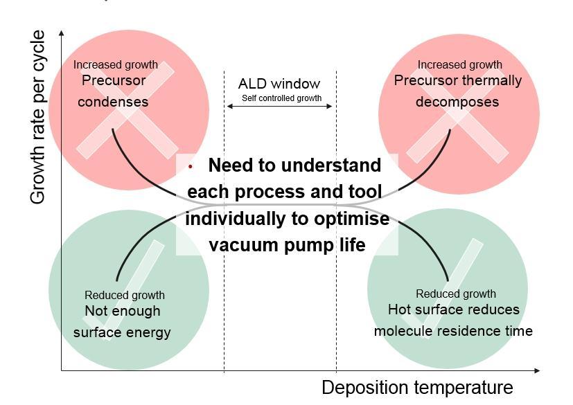
8 Fig. 2: Minimizing deposition in the tool. Source:
Plasma Etching: Atomic Scale Surface Fidelity and 2D Materials
 1 Plasma Etching: Atomic Scale Surface Fidelity and 2D Materials Thorsten Lill, Keren J. Kanarik, Samantha Tan, Meihua Shen, Alex Yoon, Eric Hudson, Yang Pan, Jeffrey Marks, Vahid Vahedi, Richard A. Gottscho
LECTURE 5 SUMMARY OF KEY IDEAS
 LECTURE 5 SUMMARY OF KEY IDEAS Etching is a processing step following lithography: it transfers a circuit image from the photoresist to materials form which devices are made or to hard masking or sacrificial
Competitive Advantages of Ontos7 Atmospheric Plasma
 Competitive Advantages of Ontos7 Atmospheric Plasma Eric Schulte Matt Phillips Keith Cooper SETNA Proprietary 1 Advantages of Ontos7 Atmospheric Plasma Process over Vacuum RIE Plasma for Die/Wafer Surface
Alternative deposition solution for cost reduction of TSV integration
 Alternative deposition solution for cost reduction of TSV integration J. Vitiello, F. Piallat, L. Bonnet KOBUS 611 rue Aristide Bergès, Z.A. de Pré Millet, Montbonnot-Saint-Martin, 38330 France Ph: +33
There's Plenty of Room at the Bottom
 There's Plenty of Room at the Bottom 12/29/1959 Feynman asked why not put the entire Encyclopedia Britannica (24 volumes) on a pin head (requires atomic scale recording). He proposed to use electron microscope
Self-study problems and questions Processing and Device Technology, FFF110/FYSD13
 Self-study problems and questions Processing and Device Technology, FFF110/FYSD13 Version 2016_01 In addition to the problems discussed at the seminars and at the lectures, you can use this set of problems
Dynamic Equipment and Process Simulation for Atomic Layer Deposition Technology
 Dynamic Equipment and Process Simulation for Atomic Layer Deposition Technology Wei Lei, Yuhong Cai, Laurent Henn-Lecordier and Gary W. Rubloff Department of Materials Science and Engineering and Institute
ALD & ALE Tutorial Speakers and Schedule
 ALD & ALE Tutorial Speakers and Schedule Sunday, July 29, 2018 1:00-1:05 Tutorial Welcome 1:05-1:50 1:50-2:35 2:35-3:20 Challenges of ALD Applications in Memory Semiconductor Devices, Choon Hwan Kim (SK
UHF-ECR Plasma Etching System for Dielectric Films of Next-generation Semiconductor Devices
 UHF-ECR Plasma Etching System for Dielectric Films of Next-generation Semiconductor Devices 1 UHF-ECR Plasma Etching System for Dielectric Films of Next-generation Semiconductor Devices Katsuya Watanabe
Film Deposition Part 1
 1 Film Deposition Part 1 Chapter 11 : Semiconductor Manufacturing Technology by M. Quirk & J. Serda Spring Semester 2013 Saroj Kumar Patra Semidonductor Manufacturing Technology, Norwegian University of
Introduction to Photolithography
 http://www.ichaus.de/news/72 Introduction to Photolithography Photolithography The following slides present an outline of the process by which integrated circuits are made, of which photolithography is
In today s lecture, we will cover:
 In today s lecture, we will cover: Chemical Vapour Deposition Atomic Layer Deposition Layer-by-Layer Polyelectrolyte Depositions 1 Nanofilms Goals for this section: Understand the chemistry of deposition
A Temporary Bonding and Debonding Technology for TSV Fabrication
 A Temporary Bonding and Debonding Technology for TSV Fabrication Taku Kawauchi, Masatoshi Shiraishi, Satoshi Okawa, Masahiro Yamamoto Tokyo Electron Ltd, Japan Taku Kawauchi, Tokyo Electron Ltd./Slide
Slide 1 Raymond Jin, Adcon Lab, Inc.
 Volume Production Proven Advanced Nanometer Slurries for CMP Applications, Capable of Recycling and Extendable to Larger Si Wafer Sizes and Future IC Technology Nodes Raymond R. Jin, X. L. Song, S. M.
EE C245 ME C218 Introduction to MEMS Design Fall 2007
 EE C245 ME C218 Introduction to MEMS Design Fall 2007 Prof. Clark T.-C. Nguyen Dept. of Electrical Engineering & Computer Sciences University of California at Berkeley Berkeley, CA 94720 Lecture 4: Film
UNIVERSITY OF CALIFORNIA College of Engineering Department of Electrical Engineering and Computer Sciences. Fall Exam 1
 UNIVERSITY OF CALIFORNIA College of Engineering Department of Electrical Engineering and Computer Sciences EECS 143 Fall 2008 Exam 1 Professor Ali Javey Answer Key Name: SID: 1337 Closed book. One sheet
Thin Film Deposition. Reading Assignments: Plummer, Chap 9.1~9.4
 Thin Film Deposition Reading Assignments: Plummer, Chap 9.1~9.4 Thermally grown Deposition Thin Film Formation Thermally grown SiO 2 Deposition SiO 2 Oxygen is from gas phase Silicon from substrate Oxide
Lecture 1: Vapour Growth Techniques
 PH3EC2 Vapour Growth and Epitaxial Growth Lecturer: Dr. Shinoj V K Lecture 1: Vapour Growth Techniques 1.1 Vapour growth The growth of single crystal materials from the vapour phase. Deposition from the
TMT4320 Nanomaterials November 10 th, Thin films by physical/chemical methods (From chapter 24 and 25)
") 1 TMT4320 Nanomaterials November 10 th, 2015 Thin films by physical/chemical methods (From chapter 24 and 25) 2 Thin films by physical/chemical methods Vapor-phase growth (compared to liquid-phase growth)
1 TMT4320 Nanomaterials November 10 th, 2015 Thin films by physical/chemical methods (From chapter 24 and 25) 2 Thin films by physical/chemical methods Vapor-phase growth (compared to liquid-phase growth)
Wafer Scale Homogeneous Bilayer Graphene Films by. Chemical Vapor Deposition
 Supporting Information for Wafer Scale Homogeneous Bilayer Graphene Films by Chemical Vapor Deposition Seunghyun Lee, Kyunghoon Lee, Zhaohui Zhong Department of Electrical Engineering and Computer Science,
ETCHING Chapter 10. Mask. Photoresist
 ETCHING Chapter 10 Mask Light Deposited Substrate Photoresist Etch mask deposition Photoresist application Exposure Development Etching Resist removal Etching of thin films and sometimes the silicon substrate
Patterning Challenges and Opportunities: Etch and Film
 Patterning Challenges and Opportunities: Etch and Film Ying Zhang, Shahid Rauf, Ajay Ahatnagar, David Chu, Amulya Athayde, and Terry Y. Lee Applied Materials, Inc. SEMICON, Taiwan 2016 Sept. 07-09, 2016,
Plasma Deposition (Overview) Lecture 1
 Lecture 1") Plasma Deposition (Overview) Lecture 1 Material Processes Plasma Processing Plasma-assisted Deposition Implantation Surface Modification Development of Plasma-based processing Microelectronics needs (fabrication
Plasma Deposition (Overview) Lecture 1 Material Processes Plasma Processing Plasma-assisted Deposition Implantation Surface Modification Development of Plasma-based processing Microelectronics needs (fabrication
Chemical Vapor Deposition (CVD)
") Chemical Vapor Deposition (CVD) source chemical reaction film substrate More conformal deposition vs. PVD t Shown here is 100% conformal deposition ( higher temp has higher surface diffusion) t step 1
Chemical Vapor Deposition (CVD) source chemical reaction film substrate More conformal deposition vs. PVD t Shown here is 100% conformal deposition ( higher temp has higher surface diffusion) t step 1
Importance of in situ Monitoring in MOCVD Process and Future Prospects
 G u e s t F o r u m Guest Forum Series of Lectures by Screening Committees of the Second Masao Horiba Awards Importance of in situ Monitoring in MOCVD Process and Future Prospects Hiroshi Funakubo Tokyo
Lecture 0: Introduction
 Lecture 0: Introduction Introduction q Integrated circuits: many transistors on one chip q Very Large Scale Integration (VLSI): bucketloads! q Complementary Metal Oxide Semiconductor Fast, cheap, low power
LEADING THE EVOLUTION OF COMPUTE MARK KACHMAREK HPC STRATEGIC PLANNING MANAGER APRIL 17, 2018
 LEADING THE EVOLUTION OF COMPUTE MARK KACHMAREK HPC STRATEGIC PLANNING MANAGER APRIL 17, 2018 INTEL S RESEARCH EFFORTS COMPONENTS RESEARCH INTEL LABS ENABLING MOORE S LAW DEVELOPING NOVEL INTEGRATION ENABLING
Thermo Scientific ICP-MS solutions for the semiconductor industry. Maximize wafer yields with ultralow elemental detection in chemicals and materials
 Thermo Scientific ICP-MS solutions for the semiconductor industry Maximize wafer yields with ultralow elemental detection in chemicals and materials Trace impurity analysis in chemicals an used in the
Process Development & Scale-Up of the AIR Technology
 Process Development & Scale-Up of the AIR Technology Lloyd Johnston, Ph.D. Vice President of Process Development & Manufacturing October 6, 2005 Pharmaceutical Industry o Delivering needed therapeutics
Gas utilization in remote plasma cleaning and stripping applications
 Gas utilization in remote plasma cleaning and stripping applications B. E. E. Kastenmeier IBM Semiconductor Research and Development Center, 2070 Rt. 52, Zip E40, Hopewell Junction, New York 12533 G. S.
EE 527 MICROFABRICATION. Lecture 25 Tai-Chang Chen University of Washington
 EE 527 MICROFABRICATION Lecture 25 Tai-Chang Chen University of Washington ION MILLING SYSTEM Kaufmann source Use e-beam to strike plasma A magnetic field applied to increase ion density Drawback Low etch
Critical Plasma Processing Parameters for Improved Strength of Wire Bonds
 Critical Plasma Processing Parameters for Improved Strength of Wire Bonds Plasma surface-treatment techniques can improve wire bonding and molding. J. Getty, L. Wood, and C. Fairfield Nordson MARCH Concord,
Modern Methods in Heterogeneous Catalysis Research: Preparation of Model Systems by Physical Methods
 Modern Methods in Heterogeneous Catalysis Research: Preparation of Model Systems by Physical Methods Methods for catalyst preparation Methods discussed in this lecture Physical vapour deposition - PLD
Agenda. 1. Atomic Layer Deposition Technology
 Agenda 1. Atomic Layer Deposition Technology 2. What is ALD? Atomic Layer Deposition is invented in 1977 by T. Suntola et al. - New Deposition Method for Electro-Luminescent Display (ZnS:Mn Thin Films)
FRAUNHOFER INSTITUTE FOR SURFACE ENGINEERING AND THIN FILMS IST ATMOSPHERIC PRESSURE PLASMA PROCESSES
 FRAUNHOFER INSTITUTE FOR SURFACE ENGINEERING AND THIN FILMS IST ATMOSPHERIC PRESSURE PLASMA PROCESSES 1 2 ATMOSPHERIC PRESSURE PLASMA PROCESSES AT THE FRAUNHOFER IST Today, atmospheric pressure plasma
Thin Wafer Handling Challenges and Emerging Solutions
 1 Thin Wafer Handling Challenges and Emerging Solutions Dr. Shari Farrens, Mr. Pete Bisson, Mr. Sumant Sood and Mr. James Hermanowski SUSS MicroTec, 228 Suss Drive, Waterbury Center, VT 05655, USA 2 Thin
Lecture 6 Plasmas. Chapters 10 &16 Wolf and Tauber. ECE611 / CHE611 Electronic Materials Processing Fall John Labram 1/68
 Lecture 6 Plasmas Chapters 10 &16 Wolf and Tauber 1/68 Announcements Homework: Homework will be returned to you on Thursday (12 th October). Solutions will be also posted online on Thursday (12 th October)
3.155J/6.152J Microelectronic Processing Technology Fall Term, 2004
 3.155J/6.152J Microelectronic Processing Technology Fall Term, 2004 Bob O'Handley Martin Schmidt Quiz Nov. 17, 2004 Ion implantation, diffusion [15] 1. a) Two identical p-type Si wafers (N a = 10 17 cm
Thin Wafer Handling Debonding Mechanisms
 Thin Wafer Handling Debonding Mechanisms Jonathan Jeauneau, Applications Manager Alvin Lee, Technology Strategist Dongshun Bai, Scientist, 3-D IC R&D Materials Outline Requirements of Thin Wafer Handling
Etching Issues - Anisotropy. Dry Etching. Dry Etching Overview. Etching Issues - Selectivity
 Etching Issues - Anisotropy Dry Etching Dr. Bruce K. Gale Fundamentals of Micromachining BIOEN 6421 EL EN 5221 and 6221 ME EN 5960 and 6960 Isotropic etchants etch at the same rate in every direction mask
4FNJDPOEVDUPS 'BCSJDBUJPO &UDI
 2010.5.4 1 Major Fabrication Steps in CMOS Process Flow UV light oxygen Silicon dioxide Silicon substrate Oxidation (Field oxide) photoresist Photoresist Coating Mask exposed photoresist Mask-Wafer Exposed
nmos IC Design Report Module: EEE 112
 nmos IC Design Report Author: 1302509 Zhao Ruimin Module: EEE 112 Lecturer: Date: Dr.Zhao Ce Zhou June/5/2015 Abstract This lab intended to train the experimental skills of the layout designing of the
1
 Process methodologies for temporary thin wafer handling solutions By Justin Furse, Technology Strategist, Brewer Science, Inc. Use of temporary bonding/debonding as part of thin wafer handling processes
EE C245 ME C218 Introduction to MEMS Design Fall 2007
 EE C245 ME C218 Introduction to MEMS Design Fall 2007 Prof. Clark T.-C. Nguyen Dept. of Electrical Engineering & Computer Sciences University of California at Berkeley Berkeley, CA 94720 Lecture 5: ALD,
MICROCHIP MANUFACTURING by S. Wolf
 by S. Wolf Chapter 15 ALUMINUM THIN-FILMS and SPUTTER-DEPOSITION 2004 by LATTICE PRESS CHAPTER 15 - CONTENTS Aluminum Thin-Films Sputter-Deposition Process Steps Physics of Sputter-Deposition Magnetron-Sputtering
IC Fabrication Technology
 IC Fabrication Technology * History: 1958-59: J. Kilby, Texas Instruments and R. Noyce, Fairchild * Key Idea: batch fabrication of electronic circuits n entire circuit, say 10 7 transistors and 5 levels
Dry Etching Zheng Yang ERF 3017, MW 5:15-6:00 pm
 Dry Etching Zheng Yang ERF 3017, email: yangzhen@uic.edu, MW 5:15-6:00 pm Page 1 Page 2 Dry Etching Why dry etching? - WE is limited to pattern sizes above 3mm - WE is isotropic causing underetching -
Supplementary materials for: Large scale arrays of single layer graphene resonators
 Supplementary materials for: Large scale arrays of single layer graphene resonators Arend M. van der Zande* 1, Robert A. Barton 2, Jonathan S. Alden 2, Carlos S. Ruiz-Vargas 2, William S. Whitney 1, Phi
Quantum Technology: Supplying the Picks and Shovels
 Quantum Technology: Supplying the Picks and Shovels Dr John Burgoyne Quantum Control Engineering: Mathematical Solutions for Industry Open for Business Event 7 th August 2014, 12.30-17.00, Isaac Newton
ISM Evolution. Elscolab. Nederland BV
 ISM Evolution Agenda Introduction Marketing Strategy ISM Concept & Technology Product Offering Applications Digital Communication and ISM Outlook 1 Agenda Introduction Marketing Strategy ISM Concept &
Microfabrication for MEMS: Part I
 Microfabrication for MEMS: Part I Carol Livermore Massachusetts Institute of Technology * With thanks to Steve Senturia, from whose lecture notes some of these materials are adapted. CL: 6.777J/2.372J
Semiconductor Technology
 Semiconductor Technology from A to Z Deposition www.halbleiter.org Contents Contents List of Figures II 1 Deposition 1 1.1 Plasma, the fourth aggregation state of a material............. 1 1.1.1 Plasma
Kavli Workshop for Journalists. June 13th, CNF Cleanroom Activities
 Kavli Workshop for Journalists June 13th, 2007 CNF Cleanroom Activities Seeing nm-sized Objects with an SEM Lab experience: Scanning Electron Microscopy Equipment: Zeiss Supra 55VP Scanning electron microscopes
Lecture 7 Oxidation. Chapter 7 Wolf and Tauber. ECE611 / CHE611 Electronic Materials Processing Fall John Labram 1/82
 Lecture 7 Oxidation Chapter 7 Wolf and Tauber 1/82 Announcements Homework: Homework will be returned to you today (please collect from me at front of class). Solutions will be also posted online on today
ORION NanoFab: An Overview of Applications. White Paper
 ORION NanoFab: An Overview of Applications White Paper ORION NanoFab: An Overview of Applications Author: Dr. Bipin Singh Carl Zeiss NTS, LLC, USA Date: September 2012 Introduction With the advancement
Taurus-Topography. Topography Modeling for IC Technology
 SYSTEMS PRODUCTS LOGICAL PRODUCTS PHYSICAL IMPLEMENTATION SIMULATION AND ANALYSIS LIBRARIES TCAD Aurora DFM WorkBench Davinci Medici Raphael Raphael-NES Silicon Early Access TSUPREM-4 Taurus-Device Taurus-Lithography
NECi Nitrate Kits FAQs
 Why use enzymes? Enzymes are catalysts that drive complex biological reactions. They happen to be excellent reagents for analytical chemistry because they are reliable, accurate, sensitive, selective,
Keywords. 1=magnetron sputtering, 2= rotatable cathodes, 3=substrate temperature, 4=anode. Abstract
 Managing Anode Effects and Substrate Heating from Rotatable Sputter Targets. F. Papa*, V. Bellido-Gonzalez**, Alex Azzopardi**, Dr. Dermot Monaghan**, *Gencoa Technical & Business Support in US, Davis,
Déposition séléctive le rêve reviens
 Willkommen Welcome Bienvenue Déposition séléctive le rêve reviens Patrik Hoffmann Michael Reinke, Yury Kuzminykh Ivo Utke, Carlos Guerra-Nunez, Ali Dabirian, Xavier Multone, Tristan Bret, Estelle Halary-Wagner,
Wafer holders. Mo- or Ta- made holders Bonding: In (Ga), or In-free (clamped) Quick and easy transfer
, or In-free (clamped) Quick and easy transfer") Wafer holders Mo- or Ta- made holders Bonding: In (Ga), or In-free (clamped) Quick and easy transfer Image: In-free, 3-inch sample holder fitting a quarter of a 2- inch wafer Reflection High Energy Electron
Wafer holders Mo- or Ta- made holders Bonding: In (Ga), or In-free (clamped) Quick and easy transfer Image: In-free, 3-inch sample holder fitting a quarter of a 2- inch wafer Reflection High Energy Electron
EE143 Fall 2016 Microfabrication Technologies. Lecture 6: Thin Film Deposition Reading: Jaeger Chapter 6
 EE143 Fall 2016 Microfabrication Technologies Lecture 6: Thin Film Deposition Reading: Jaeger Chapter 6 Prof. Ming C. Wu wu@eecs.berkeley.edu 511 Sutardja Dai Hall (SDH) 1 Vacuum Basics Units 1 atmosphere
THE APPLICATION OF PROCESS MASS SPECTROMETRY TO FUMED SILICA PRODUCTION
 JPACSM 5 Process Analytical Chemistry THE APPLICATION OF PROCESS MASS SPECTROMETRY TO FUMED SILICA PRODUCTION Peter Traynor and Steven Trimuar Thermo Electron Corporation Houston, TX Robert G. Wright Thermo
Defect management and control. Tsuyoshi Moriya, PhD Senior Manager Tokyo Electron Limited
 Defect management and control Tsuyoshi Moriya, PhD Senior Manager Tokyo Electron Limited Background Case study: A maintainer has good hands Only he achieved good yield for every maintenance But... He could
Layer-modulated synthesis of uniform tungsten disulfide nanosheet using gas-phase precursors.
 Layer-modulated synthesis of uniform tungsten disulfide nanosheet using gas-phase precursors. Jusang Park * Hyungjun Kim School of Electrical and Electronics Engineering, Yonsei University, 262 Seongsanno,
 Miniaturized Sensor for the Detection of Environmental Pollutants Alexander Graf 1, Ronald Stübner 1, Christian Kunath 1, Sebastian Meyer 1, Harald Schenk 1 1 Fraunhofer Institute for Photonic Microsystems
Equipment Innovation Team, Memory Fab. Center, Samsung Electronics Co. Ltd. San#16, Banwol, Taean, Hwansung, Kyungki, , Republic of Korea
 Solid State Phenomena Vols. 103-104 (2005) pp 63-66 Online available since 2005/Apr/01 at www.scientific.net (2005) Trans Tech Publications, Switzerland doi:10.4028/www.scientific.net/ssp.103-104.63 Development
Supporting Information for: Sustained sub-60 mv/decade switching via the negative capacitance effect in MoS 2 transistors
 Supporting Information for: Sustained sub-60 mv/decade switching via the negative capacitance effect in MoS 2 transistors Felicia A. McGuire 1, Yuh-Chen Lin 1, Katherine Price 1, G. Bruce Rayner 2, Sourabh
Device Fabrication: Etch
 Device Fabrication: Etch 1 Objectives Upon finishing this course, you should able to: Familiar with etch terminology Compare wet and dry etch processes processing and list the main dry etch etchants Become
Transistor and Integrated Circuits: History
 Course Objective Review and practice fundamental chemical engineering concepts (mass, energy, and momentum transport coupled with heterogeneous and homogeneous reactions and thermodynamics). Apply these
SUPPLEMENTARY INFORMATION
 doi:.38/nature09979 I. Graphene material growth and transistor fabrication Top-gated graphene RF transistors were fabricated based on chemical vapor deposition (CVD) grown graphene on copper (Cu). Cu foil
PLW2835ACC Series. Product Datasheet. Bulb Wall Light Floor Lamp Tube Lighting
 V.8/17 PLW2835ACC Series Product Datasheet Bulb Wall Light Floor Lamp Tube Lighting General Lighting Introduction The PLW2835ACC series offer ultra-high luminous efficacy combined with the flexibility
Chip-Scale Mass Spectrometers for Portable Gas Analyzers Luis Fernando Velásquez-García. A. I. Akinwande, K. Cheung, and L.-Y Chen.
 Chip-Scale Mass Spectrometers for Portable Gas Analyzers Luis Fernando Velásquez-García. A. I. Akinwande, K. Cheung, and L.-Y Chen. Microsystems Technology Laboratories (MTL) lfvelasq@mit.edu November
Step Coverage by ALD Films: Theory and Examples
 Step Coverage by ALD Films: Theory and Examples of Ideal and Non-Ideal Reactions Roy G. Gordon Cambridge, MA 1 L Step Coverage in Holes with High Aspect Ratio Step coverage = (b/a) x 100% a Aspect ratio
Solliance. Perovskite based PV (PSC) Program. TKI Urban Energy Days l e d b y i m e c, E C N a n d T N O
 Program. TKI Urban Energy Days l e d b y i m e c, E C N a n d T N O") Solliance Perovskite based PV (PSC) Program TKI Urban Energy Days - 2017-06-21 l e d b y i m e c, E C N a n d T N O 2 Bringing together research and industry Providing insight and know-how to all partners
Solliance Perovskite based PV (PSC) Program TKI Urban Energy Days - 2017-06-21 l e d b y i m e c, E C N a n d T N O 2 Bringing together research and industry Providing insight and know-how to all partners
I. INTRODUCTION. 127 J. Vac. Sci. Technol. B 15(1), Jan/Feb X/97/15(1)/127/6/$ American Vacuum Society 127
, Jan/Feb X/97/15(1)/127/6/$ American Vacuum Society 127") Real-time process sensing and metrology in amorphous and selective area silicon plasma enhanced chemical vapor deposition using in situ mass spectrometry Ashfaqul I. Chowdhury, a) Walter W. Read, a) Gary
Real-time process sensing and metrology in amorphous and selective area silicon plasma enhanced chemical vapor deposition using in situ mass spectrometry Ashfaqul I. Chowdhury, a) Walter W. Read, a) Gary
Nanoparticles for coatings. Why is reality so much less than the promise? Professor Steven Abbott R&T Director MacDermid Autotype Ltd
 Nanoparticles for coatings. Why is reality so much less than the promise? Professor Steven Abbott R&T Director MacDermid Autotype Ltd Background to the problem MacDermid Autotype make high quality coated
Manufacturable AlGaAs/GaAs HBT Implant Isolation Process Using Doubly Charged Helium
 Manufacturable AlGaAs/GaAs HBT Implant Isolation Process Using Doubly Charged Helium ABSTRACT Rainier Lee, Shiban Tiku, and Wanming Sun Conexant Systems 2427 W. Hillcrest Drive Newbury Park, CA 91320 (805)
Brigham Young University. Infiltration of CNT-M Microstructures using CVD and ALD Presented by: Collin Brown, Jason Kyle Anderson
 Infiltration of CNT-M Microstructures using CVD and ALD Presented by: Collin Brown, Jason Kyle Anderson October 31st, 2013 Acknowledgments Jason Kyle Anderson for his help in getting the system to work
Cost of Ownership Considerations for Maskless Lithography
 Accelerating the next technology revolution Cost of Ownership Considerations for Maskless Lithography Lloyd C. Litt, SEMATECH Andrea F. Wüest, SEMATECH Copyright 2008 SEMATECH, Inc. SEMATECH, and the SEMATECH
Atomic layer deposition of titanium nitride
 Atomic layer deposition of titanium nitride Jue Yue,version4, 04/26/2015 Introduction Titanium nitride is a hard and metallic material which has found many applications, e.g.as a wear resistant coating[1],
Lecture 18: Microfluidic MEMS, Applications
 MECH 466 Microelectromechanical Systems University of Victoria Dept. of Mechanical Engineering Lecture 18: Microfluidic MEMS, Applications 1 Overview Microfluidic Electrokinetic Flow Basic Microfluidic
Real-Time Chemical Sensing for Advanced Process Control in ALD
 Real-Time Chemical Sensing for Advanced Process Control in ALD Gary W. Rubloff 1, Laurent Henn-Lecordier 2, and Wei Lei 3 University of Maryland 1 Director, Maryland Center for Integrated Nano Science
Nanofabrication Lab Process Development for High-k Dielectrics
 Nanofabrication Lab Process Development for Highk Dielectrics Each lab group consists of 4 to 5 students. The dates of these Labs are: Lab 1 Date 14.02.2013 Time: 812 am Lab 2 Date 14.02.2013 Time: 15
CVD: General considerations.
 CVD: General considerations. PVD: Move material from bulk to thin film form. Limited primarily to metals or simple materials. Limited by thermal stability/vapor pressure considerations. Typically requires
Chemical Vapor Deposition *
 OpenStax-CNX module: m25495 1 Chemical Vapor Deposition * Andrew R. Barron This work is produced by OpenStax-CNX and licensed under the Creative Commons Attribution License 3.0 note: This module was developed
PLW2835EKA Series. Product Datasheet. Floor Light
 PLW2835EKA Series Product Datasheet Bulb Wall Light Floor Light Tube Light General Lighting Introduction The PLW2835EKA series offer ultra-high luminous efficacy combined with the flexibility in design
Defense Technical Information Center Compilation Part Notice
 UNCLASSIFIED Defense Technical Information Center Compilation Part Notice ADP013065 TITLE: Two-Dimensional Photonic Crystal Fabrication Using Fullerene Films DISTRIBUTION: Approved for public release,
EE-612: Lecture 22: CMOS Process Steps
 EE-612: Lecture 22: CMOS Process Steps Mark Lundstrom Electrical and Computer Engineering Purdue University West Lafayette, IN USA Fall 2006 NCN www.nanohub.org Lundstrom EE-612 F06 1 outline 1) Unit Process
Advances in Back-side Via Etching of SiC for GaN Device Applications
 Advances in Back-side Via Etching of SiC for GaN Device Applications Anthony Barker, Kevin Riddell, Huma Ashraf & Dave Thomas SPTS Technologies, Ringland Way, Newport NP18 2TA, UK, dave.thomas@spts.com,
UNIT 3. By: Ajay Kumar Gautam Asst. Prof. Dev Bhoomi Institute of Technology & Engineering, Dehradun
 UNIT 3 By: Ajay Kumar Gautam Asst. Prof. Dev Bhoomi Institute of Technology & Engineering, Dehradun 1 Syllabus Lithography: photolithography and pattern transfer, Optical and non optical lithography, electron,
PARTICLE MEASUREMENT IN CLEAN ROOM TECHNOLOGY
 WHITEPAPER ENGLISH PARTICLE MEASUREMENT IN CLEAN ROOM TECHNOLOGY PARTICLE MEASUREMENT Particle measurement in cleanrooms. WP1508006-0100-EN, V1R0, 2015-08 PARTICLE MEASUREMENT IN CLEAN ROOM TECHNOLOGY
Explosion Properties of Highly Concentrated Ozone Gas. 1 Iwatani International Corporation, Katsube, Moriyama, Shiga , Japan
 Explosion Properties of Highly Concentrated Ozone Gas Kunihiko Koike 1*, Masaharu Nifuku 2, Koichi Izumi 1, Sadaki Nakamura 1, Shuzo Fujiwara 2 and Sadashige Horiguchi 2 1 Iwatani International Corporation,
Technology Improvement and Fault TCP Etch Chamber and a Dual Frequency Oxide Etch Chamber
 Technology Improvement and Fault Detection @ TCP Etch Chamber and a Dual Frequency Oxide Etch Chamber Russell Benson, Micron Daniel Steckert, Micron Lutz Eichhorn, Plasmetrex Michael Klick, Plasmetrex
Abstract No. 48. Multi-step oxidation of mineral samples by borate fusion Dirk Töwe, HRT Fusion GmbH
 Abstract No. 48 Multi-step oxidation of mineral samples by borate fusion Dirk Töwe, HRT Fusion GmbH Service laboratories performing borate fusion sample preparation for XRF analysis are exposed to a very
Forecasting Time Frames Using Gann Angles By Jason Sidney
 Forecasting Time Frames Using Gann Angles By Jason Sidney In the previous lesson, we looked at how Gann Angles can be used in conjunction with eighths and third retracements. In that lesson you were shown
NGSS. Science Items Grade 5 Middle School High School. Table of Contents. Grade Middle School... 5 High School... 10
 NGSS Science Items Grade 5 Middle School High School As printed in Translating the NGSS for Classroom Instruction (Bybee, 2013) Table of Contents Grade 5...1 Middle School.... 5 High School... 10 Grade
6.5 Optical-Coating-Deposition Technologies
 92 Chapter 6 6.5 Optical-Coating-Deposition Technologies The coating process takes place in an evaporation chamber with a fully controlled system for the specified requirements. Typical systems are depicted
Dynamization evolution of Dry Etch Tools in Semiconductor Device Fabrication Gordon Cameron Intel Corp (November 2005)
") Dynamization evolution of Dry Etch Tools in Semiconductor Device Fabrication Gordon Cameron Intel Corp (November 2005) Abstract Engineering Systems follow recognized trends of evolution; the main parameters
Dynamization evolution of Dry Etch Tools in Semiconductor Device Fabrication Gordon Cameron Intel Corp (November 2005) Abstract Engineering Systems follow recognized trends of evolution; the main parameters
Supplementary Information. Rapid Stencil Mask Fabrication Enabled One-Step. Polymer-Free Graphene Patterning and Direct
 Supplementary Information Rapid Stencil Mask Fabrication Enabled One-Step Polymer-Free Graphene Patterning and Direct Transfer for Flexible Graphene Devices Keong Yong 1,, Ali Ashraf 1,, Pilgyu Kang 1,
Lecture 11. Etching Techniques Reading: Chapter 11. ECE Dr. Alan Doolittle
 Lecture 11 Etching Techniques Reading: Chapter 11 Etching Techniques Characterized by: 1.) Etch rate (A/minute) 2.) Selectivity: S=etch rate material 1 / etch rate material 2 is said to have a selectivity