New Material Design and Device Simulation Tool. Dr. Gong Kui HZWTECH
|
|
|
- Buddy Ferguson
- 5 years ago
- Views:
Transcription
 股份有限公司 HONGZHIWEI")
1 New Material Design and Device Simulation Tool Dr. Gong Kui HZWTECH 鸿之微科技 ( 上海 ) 股份有限公司 HONGZHIWEI TECHNOLOGY(SHANGHAI) CO.,LTD
2 outline Atomistic-TCAD:new devices simulation tool Applications of Atomistic-TCAD What Atomistic-TCAD can do in future?
3 Atomistic-TCAD:New Device Simulation tool


")


4 New TCAD for Device: materials + quantum transport science engineering new quantum mechanics math, physics atomic simulations materials, chemistry, math, physics device modeling < 10nm (10000 atoms) Semi-empirical device modeling device parameters TCAD Atomistic-TCAD: quantitative predictions from atomic first principles without free parameter for realistic device structures.
5 New Characters of Devices Device performance not stability F.L. Yang et al., in VLSI Technol. Tech. Symp. Dig., pp. 208, June 2007.

6 New Characters of Devices Today s Device Process Design Traditional TCAD Foundries

7 New Characters of Devices Need more and more parameters


8 Challenge of device design: hard to get parameters Traditional TCAD: large number of parameters 1328 pages of parameters! Picture from Mansun Chan

9 Challenge of device design: hard to get parameters Quantum effect dominate transport properties


10 Challenge of device design: hard to get parameters New materials? Picture from Hong Guo

11 Challenge of device design: The complexity of the interface Defect / lattice mismatch / grain boundary lead to more problems defect mismatch

12 Challenge of device design: Heat conduction More heat transport problems in the scales
")
13 Atomistic-TCAD:New Device Simulation tool Quantum simulator: Full quantum description of electronic transport First principle prediction of material properties NEGF-DFT simulation I-V,C-V Curve (Atomistic TCAD) Atomistic-TCAD
14 Atomistic-TCAD:New Device Simulation tool How atomistic-tcad work? System left lead cell decomposed Central cell construct right lead cell Cell shape Atoms in cell Full quantum description of electronic transport First principle prediction of material properties NEGF-DFT simulation


15 Atomistic-TCAD:New Device Simulation tool FDSOI simulation Atomic Structure I V curves C V curves
16 Application of Atomistic-TCAD

17 Application of Atomistic-TCAD IEEE Trans. Elec. Dev. 60, 3527 (2013) atomistic-tcad vs. traditional TCAD 3D FETs, strain different surfaces, mobility, other materials, defects.


18 Application of Atomistic-TCAD :Design MOSFET with new material IEEE Trans. Elec. Dev. 61, 11 (2014)

19 Application of Atomistic-TCAD : Design TFET with new material


20 Application of Atomistic-TCAD :Design TFET with new material P type Source Gate HfO 2 N type Drain MoTe 2 SnS 2 HfO 2 Gate Monolayer TMDCs heterojunction with very low SS value


21 Application of Atomistic-TCAD :Design MTJ device Fe MgO Fe 1, 2, 3,...11,12,13 Red: x% on both layers 1 and 13. Black: 3% on 1, x% on 13. TMR = Green: 3% on 1, x% on 7, for a 7- layer MgO. Youqi Ke, Ke Xia and Hong Guo, PRL 105, (2010).
.")
22 Application of Atomistic-TCAD: I off vs. dopant position little difference in I OFF is found I OFF decreases dramatically with increasing channel length. Transport properties depend sensitively on where the impurities are distributed. The ratio between G MAX and G MIN increases with L. Maasson, Zhu, H.G. (2011).


23 Atomistic-TCAD: High-k material design of HfO2 Gate Oxides Proposed structure to reduce tunneling leakage by rich oxygen J. Appl. Phys. 2014, 116,


24 Application of Atomistic-TCAD: Electromigration of copper Phosphorus to be an optimal surface electromigration inhibitor on Cu surface.

25 Application of Atomistic-TCAD: Investigate copper interconnect


26 Application of Atomistic-TCAD: Investigate copper interconnect (1) Doping of Cu surfaces Vision: Surface doping flattens the equipotential surface specular scattering Most exciting result: Al barrier coating reduces resistivity by 20%. (2) Doping of Cu grain boundaries Vision: Grain boundary doping reduces potential variation high boundary transmission This year s focus: First-principles prediction of resistance for many Cu grain boundaries vs doping concentration and doping element. Most promising : Doping reduces resistance of low-symmetry boundaries by up to 50%.
27 Conclusion: What Atomistic-TCAD can do in future? Extraction of physical quantity of Model; Extraction of electronic transport parameters; Design of dielectric layer; Research the interface effecting of device; Channel design and leakage control; Simulation the doping behavior; Analysis the effecting of stress in transport; Analysis of heat transport; Improvement or innovation of device structure; Process improvement or innovation; New materials (III-V) application;
28 THANKS! 鸿之微科技 ( 上海 ) 股份有限公司 HONGZHIWEI TECHNOLOYGY(SHANGHAI) CO.,LTD
Computational electronics from atomic principles - basics of electronic transport. Hong Guo
 Computational electronics from atomic principles - basics of electronic transport Hong Guo Center for the Physics of Materials and Dept. of Physics, McGill Univ., Montreal, Canada Introduction: need for
Modeling Transport in Heusler-based Spin Devices
 Modeling Transport in Heusler-based Spin Devices Gautam Shine (Stanford) S. Manipatruni, A. Chaudhry, D. E. Nikonov, I. A. Young (Intel) Electronic Structure Extended Hückel theory Application to Heusler
Current mechanisms Exam January 27, 2012
 Current mechanisms Exam January 27, 2012 There are four mechanisms that typically cause currents to flow: thermionic emission, diffusion, drift, and tunneling. Explain briefly which kind of current mechanisms
Steep Slope Transistors beyond the Tunnel FET concept. David Esseni, University of Udine
 Steep Slope Transistors beyond the Tunnel FET concept David Esseni, University of Udine Overcome Boltzmann s Tyranny Sub-threshold swing may be expressed as V g = φ s V S/D G In MOSFETs: - second term
Electronics with 2D Crystals: Scaling extender, or harbinger of new functions?
 Electronics with 2D Crystals: Scaling extender, or harbinger of new functions? 1 st Workshop on Data Abundant Systems Technology Stanford, April 2014 Debdeep Jena (djena@nd.edu) Electrical Engineering,
Graphene for future VLSI
 Graphene for future VLSI greg.yeric@arm.com Fellow ARM Research Why did the semiconductor industry get so excited about graphene? 2 The problem with planar MOSFETs Gate Source Drain Substrate One-dimensional
Effect of the High-k Dielectric/Semiconductor Interface on Electronic Properties in Ultra-thin Channels
 Effect of the High-k Dielectric/Semiconductor Interface on Electronic Properties in Ultra-thin Channels Evan Wilson, Daniel Valencia, Mark J. W. Rodwell, Gerhard Klimeck and Michael Povolotskyi Electrical
Theory of Hydrogen-Related Levels in Semiconductors and Oxides
 Theory of Hydrogen-Related Levels in Semiconductors and Oxides Chris G. Van de Walle Materials Department University of California, Santa Barbara Acknowledgments Computations J. Neugebauer (Max-Planck-Institut,
Ultra-Scaled InAs HEMTs
 Performance Analysis of Ultra-Scaled InAs HEMTs Neerav Kharche 1, Gerhard Klimeck 1, Dae-Hyun Kim 2,3, Jesús. A. del Alamo 2, and Mathieu Luisier 1 1 Network for Computational ti Nanotechnology and Birck
Nanocarbon Interconnects - From 1D to 3D
 Nanocarbon Interconnects - From 1D to 3D Cary Y. Yang Santa Clara University Outline Introduction CNT as 1D interconnect structure CNT-graphene as all-carbon 3D interconnect Summary Device Scaling driven
Computational Model of Edge Effects in Graphene Nanoribbon Transistors
 Nano Res (2008) 1: 395 402 DOI 10.1007/s12274-008-8039-y Research Article 00395 Computational Model of Edge Effects in Graphene Nanoribbon Transistors Pei Zhao 1, Mihir Choudhury 2, Kartik Mohanram 2,
Journal of Electron Devices, Vol. 18, 2013, pp JED [ISSN: ]
![Journal of Electron Devices, Vol. 18, 2013, pp JED [ISSN: ]](/thumbs/86/93990983.jpg "Journal of Electron Devices, Vol. 18, 2013, pp JED [ISSN: ]") DrainCurrent-Id in linearscale(a/um) Id in logscale Journal of Electron Devices, Vol. 18, 2013, pp. 1582-1586 JED [ISSN: 1682-3427 ] SUITABILITY OF HIGH-k GATE DIELECTRICS ON THE DEVICE PERFORMANCE AND
DrainCurrent-Id in linearscale(a/um) Id in logscale Journal of Electron Devices, Vol. 18, 2013, pp. 1582-1586 JED [ISSN: 1682-3427 ] SUITABILITY OF HIGH-k GATE DIELECTRICS ON THE DEVICE PERFORMANCE AND
MSE 310/ECE 340: Electrical Properties of Materials Fall 2014 Department of Materials Science and Engineering Boise State University
 MSE 310/ECE 340: Electrical Properties of Materials Fall 2014 Department of Materials Science and Engineering Boise State University Practice Final Exam 1 Read the questions carefully Label all figures
Imaginary Band Structure and Its Role in Calculating Transmission Probability in Semiconductors
 Imaginary Band Structure and Its Role in Calculating Transmission Probability in Semiconductors Jamie Teherani Collaborators: Paul Solomon (IBM), Mathieu Luisier(Purdue) Advisors: Judy Hoyt, DimitriAntoniadis
Challenges in the introduction of Band to Band tunneling in semiclassical models for Tunnel-FETs. DIEGM - University of Udine, IU.
 Challenges in the introduction of Band to Band tunneling in semiclassical models for Tunnel-FETs, L.De Michielis*, M.Iellina and L.Selmi DIEGM - University of Udine, IU.NET *EPFL Outline Context Quantum
OMEN an atomistic and full-band quantum transport simulator for post-cmos nanodevices
 Purdue University Purdue e-pubs Other Nanotechnology Publications Birck Nanotechnology Center 8-18-28 OMEN an atomistic and full-band quantum transport simulator for post-cmos nanodevices Mathieu Luisier
Analysis of InAs Vertical and Lateral Band-to-Band Tunneling. Transistors: Leveraging Vertical Tunneling for Improved Performance
 Analysis of InAs Vertical and Lateral Band-to-Band Tunneling Transistors: Leveraging Vertical Tunneling for Improved Performance Kartik Ganapathi, Youngki Yoon and Sayeef Salahuddin a) Department of Electrical
arxiv: v2 [cond-mat.mtrl-sci] 11 Sep 2016
![arxiv: v2 [cond-mat.mtrl-sci] 11 Sep 2016](/thumbs/73/68883795.jpg "arxiv: v2 [cond-mat.mtrl-sci] 11 Sep 2016") arxiv:1608.05057v2 [cond-mat.mtrl-sci] 11 ep 2016 Transport in vertically stacked hetero-structures from 2D materials Fan Chen, Hesameddin Ilatikhameneh, Yaohua Tan, Daniel Valencia, Gerhard Klimeck and
arxiv:1608.05057v2 [cond-mat.mtrl-sci] 11 ep 2016 Transport in vertically stacked hetero-structures from 2D materials Fan Chen, Hesameddin Ilatikhameneh, Yaohua Tan, Daniel Valencia, Gerhard Klimeck and
Scaling Issues in Planar FET: Dual Gate FET and FinFETs
 Scaling Issues in Planar FET: Dual Gate FET and FinFETs Lecture 12 Dr. Amr Bayoumi Fall 2014 Advanced Devices (EC760) Arab Academy for Science and Technology - Cairo 1 Outline Scaling Issues for Planar
+ V gate M O. Trend: As k, E g. Part 6: High Dielectric Constant (k), Gate Electrode, & Channel Materials. Bandgap versus Dielectric Constant (k) k k
, Gate Electrode, & Channel Materials. Bandgap versus Dielectric Constant (k) k k") Part 6: High Dielectric Constant (k), Gate Electrode, & Channel Materials O 2 gate oxide is approaching physical limits Thickness & Current M O S poly-crystalline V Source W Source Contact Insulator n
Part 6: High Dielectric Constant (k), Gate Electrode, & Channel Materials O 2 gate oxide is approaching physical limits Thickness & Current M O S poly-crystalline V Source W Source Contact Insulator n
How a single defect can affect silicon nano-devices. Ted Thorbeck
 How a single defect can affect silicon nano-devices Ted Thorbeck tedt@nist.gov The Big Idea As MOS-FETs continue to shrink, single atomic scale defects are beginning to affect device performance Gate Source
A final review session will be offered on Thursday, May 10 from 10AM to 12noon in 521 Cory (the Hogan Room).
.") A final review session will be offered on Thursday, May 10 from 10AM to 12noon in 521 Cory (the Hogan Room). The Final Exam will take place from 12:30PM to 3:30PM on Saturday May 12 in 60 Evans.» All of
A final review session will be offered on Thursday, May 10 from 10AM to 12noon in 521 Cory (the Hogan Room). The Final Exam will take place from 12:30PM to 3:30PM on Saturday May 12 in 60 Evans.» All of
Quantum Mechanical Simulation for Ultra-thin High-k Gate Dielectrics Metal Oxide Semiconductor Field Effect Transistors
 Mechanical Simulation for Ultra-thin High-k Gate Dielectrics Metal Oxide Semiconductor Field Effect Transistors Shih-Ching Lo 1, Yiming Li 2,3, and Jyun-Hwei Tsai 1 1 National Center for High-Performance
Lecture 20: Semiconductor Structures Kittel Ch 17, p , extra material in the class notes
 Lecture 20: Semiconductor Structures Kittel Ch 17, p 494-503, 507-511 + extra material in the class notes MOS Structure Layer Structure metal Oxide insulator Semiconductor Semiconductor Large-gap Semiconductor
Impact of intrinsic deformations on the negative differential resistance of monolayer MoS 2 ultrashort channel MOSFET
 Impact of intrinsic deformations on the negative differential resistance of monolayer MoS 2 ultrashort channel MOSFET Amretashis Sengupta*, Santanu Mahapatra Nano-Scale Device Research Laboratory, Dept.
Modeling and Computation of Gate Tunneling Current through Ultra Thin Gate Oxides in Double Gate MOSFETs with Ultra Thin Body Silicon Channel
 Modeling and Computation of Gate Tunneling Current through Ultra Thin Gate Oxides in Double Gate MOSFETs with Ultra Thin Body Silicon Channel Bhadrinarayana L V 17 th July 2008 Microelectronics Lab, Indian
Understanding the effect of n-type and p-type doping in the channel of graphene nanoribbon transistor
 Bull. Mater. Sci., Vol. 39, No. 5, September 2016, pp. 1303 1309. DOI 10.1007/s12034-016-1277-9 c Indian Academy of Sciences. Understanding the effect of n-type and p-type doping in the channel of graphene
Influence of structural and doping parameter variations on Si and Si 1 x Ge x double gate tunnel FETs: An analysis for RF performance enhancement
 Pramana J. Phys. (2018) 91:2 https://doi.org/10.1007/s12043-018-1577-2 Indian Academy of Sciences Influence of structural and doping parameter variations on Si and Si 1 x Ge x double gate tunnel FETs:
Stretching the Barriers An analysis of MOSFET Scaling. Presenters (in order) Zeinab Mousavi Stephanie Teich-McGoldrick Aseem Jain Jaspreet Wadhwa
 Zeinab Mousavi Stephanie Teich-McGoldrick Aseem Jain Jaspreet Wadhwa") Stretching the Barriers An analysis of MOSFET Scaling Presenters (in order) Zeinab Mousavi Stephanie Teich-McGoldrick Aseem Jain Jaspreet Wadhwa Why Small? Higher Current Lower Gate Capacitance Higher
Stretching the Barriers An analysis of MOSFET Scaling Presenters (in order) Zeinab Mousavi Stephanie Teich-McGoldrick Aseem Jain Jaspreet Wadhwa Why Small? Higher Current Lower Gate Capacitance Higher
Quantum Phenomena & Nanotechnology (4B5)
") Quantum Phenomena & Nanotechnology (4B5) The 2-dimensional electron gas (2DEG), Resonant Tunneling diodes, Hot electron transistors Lecture 11 In this lecture, we are going to look at 2-dimensional electron
Quantum Phenomena & Nanotechnology (4B5) The 2-dimensional electron gas (2DEG), Resonant Tunneling diodes, Hot electron transistors Lecture 11 In this lecture, we are going to look at 2-dimensional electron
From Physics to Power, Performance, and Parasitics
 From Physics to Power, Performance, and Parasitics The GTS-Team Global TCAD Solutions GmbH, Böserndorferstraße 1/12, 1010 Vienna, Austria O. Baumgartner et al. (GTS) GTS 1 / 25 Scales, methods, hierarchies
Lecture 9. Strained-Si Technology I: Device Physics
 Strain Analysis in Daily Life Lecture 9 Strained-Si Technology I: Device Physics Background Planar MOSFETs FinFETs Reading: Y. Sun, S. Thompson, T. Nishida, Strain Effects in Semiconductors, Springer,
Threshold voltage shift of heteronanocrystal floating gate flash memory
 JOURNAL OF APPLIED PHYSICS 97, 034309 2005 Threshold voltage shift of heteronanocrystal floating gate flash memory Yan Zhu, Dengtao Zhao, Ruigang Li, and Jianlin Liu a Quantum Structures Laboratory, Department
Available online at ScienceDirect. Procedia Materials Science 11 (2015 )
") Available online at www.sciencedirect.com ScienceDirect Procedia Materials Science 11 (2015 ) 287 292 5th International Biennial Conference on Ultrafine Grained and Nanostructured Materials, UFGNSM15 Tunneling
Available online at www.sciencedirect.com ScienceDirect Procedia Materials Science 11 (2015 ) 287 292 5th International Biennial Conference on Ultrafine Grained and Nanostructured Materials, UFGNSM15 Tunneling
Drift-diffusion model for single layer transition metal dichalcogenide field-effect transistors
 Drift-diffusion model for single layer transition metal dichalcogenide field-effect transistors David Jiménez Departament d'enginyeria Electrònica, Escola d'enginyeria, Universitat Autònoma de Barcelona,
GaN based transistors
 GaN based transistors S FP FP dielectric G SiO 2 Al x Ga 1-x N barrier i-gan Buffer i-sic D Transistors "The Transistor was probably the most important invention of the 20th Century The American Institute
IBM Research Report. Quantum-Based Simulation Analysis of Scaling in Ultra-Thin Body Device Structures
 RC23248 (W0406-088) June 16, 2004 Electrical Engineering IBM Research Report Quantum-Based Simulation Analysis of Scaling in Ultra-Thin Body Device Structures Arvind Kumar, Jakub Kedzierski, Steven E.
Tunnel-FET: bridging the gap between prediction and experiment through calibration
 Tunnel-FET: bridging the gap between prediction and experiment through calibration Anne Verhulst Quentin Smets, Jasper Bizindavyi, Mazhar Mohammed, Devin Verreck, Salim El Kazzi, Alireza Alian, Yves Mols,
Electron spin transport in Magnetic Multilayers and Carbon Materials. Kurt Stokbro CEO, Founder QuantumWise A/S (Copenhagen, Denmark)
") Electron spin transport in Magnetic Multilayers and Carbon Materials Kurt Stokbro CEO, Founder QuantumWise A/S (Copenhagen, Denmark) www.quantumwise.com (kurt.stokbro@quantumwise.com) Outline Methodology
Electron spin transport in Magnetic Multilayers and Carbon Materials Kurt Stokbro CEO, Founder QuantumWise A/S (Copenhagen, Denmark) www.quantumwise.com (kurt.stokbro@quantumwise.com) Outline Methodology
Supporting Information
 Supporting Information Monolithically Integrated Flexible Black Phosphorus Complementary Inverter Circuits Yuanda Liu, and Kah-Wee Ang* Department of Electrical and Computer Engineering National University
EE410 vs. Advanced CMOS Structures
 EE410 vs. Advanced CMOS Structures Prof. Krishna S Department of Electrical Engineering S 1 EE410 CMOS Structure P + poly-si N + poly-si Al/Si alloy LPCVD PSG P + P + N + N + PMOS N-substrate NMOS P-well
Fig The electron mobility for a-si and poly-si TFT.
 Fig. 1-1-1 The electron mobility for a-si and poly-si TFT. Fig. 1-1-2 The aperture ratio for a-si and poly-si TFT. 33 Fig. 1-2-1 All kinds defect well. (a) is the Dirac well. (b) is the repulsive Columbic
Classification of Solids
 Classification of Solids Classification by conductivity, which is related to the band structure: (Filled bands are shown dark; D(E) = Density of states) Class Electron Density Density of States D(E) Examples
Ab initio Berechungen für Datenbanken
 J Ab initio Berechungen für Datenbanken Jörg Neugebauer University of Paderborn Lehrstuhl Computational Materials Science Computational Materials Science Group CMS Group Scaling Problem in Modeling length
Bipolar quantum corrections in resolving individual dopants in atomistic device simulation
 Superlattices and Microstructures 34 (2003) 327 334 www.elsevier.com/locate/superlattices Bipolar quantum corrections in resolving individual dopants in atomistic device simulation Gareth Roy, Andrew R.
Negative Capacitance Tunnel Field Effect Transistor: A Novel Device with Low Subthreshold Swing and High ON Current
 Negative Capacitance Tunnel Field Effect Transistor: A Novel Device with Low Subthreshold Swing and High ON Current Nadim Chowdhury, S. M. Farhaduzzaman Azad and Quazi D.M. Khosru Department of Electrical
Indium arsenide quantum wire trigate metal oxide semiconductor field effect transistor
 JOURNAL OF APPLIED PHYSICS 99, 054503 2006 Indium arsenide quantum wire trigate metal oxide semiconductor field effect transistor M. J. Gilbert a and D. K. Ferry Department of Electrical Engineering and
Towards Atomistic Simulations of the Electro-Thermal Properties of Nanowire Transistors Mathieu Luisier and Reto Rhyner
 Towards Atomistic Simulations of the Electro-Thermal Properties of Nanowire Transistors Mathieu Luisier and Reto Rhyner Integrated Systems Laboratory ETH Zurich, Switzerland Outline Motivation Electron
ESE 570: Digital Integrated Circuits and VLSI Fundamentals
 ESE 570: Digital Integrated Circuits and VLSI Fundamentals Lec 4: January 23, 2018 MOS Transistor Theory, MOS Model Penn ESE 570 Spring 2018 Khanna Lecture Outline! CMOS Process Enhancements! Semiconductor
ATOMIC-SCALE THEORY OF RADIATION-INDUCED PHENOMENA
 ATOMIC-SCALE THEORY OF RADIATION-INDUCED PHENOMENA OVERVIEW OF THE LAST FIVE YEARS AND NEW RESULTS Sokrates T. Pantelides Department of Physics and Astronomy, Vanderbilt University, Nashville, TN The theory
CHAPTER 5 EFFECT OF GATE ELECTRODE WORK FUNCTION VARIATION ON DC AND AC PARAMETERS IN CONVENTIONAL AND JUNCTIONLESS FINFETS
 98 CHAPTER 5 EFFECT OF GATE ELECTRODE WORK FUNCTION VARIATION ON DC AND AC PARAMETERS IN CONVENTIONAL AND JUNCTIONLESS FINFETS In this chapter, the effect of gate electrode work function variation on DC
Overview of Modeling and Simulation TCAD - FLOOPS / FLOODS
 Overview of Modeling and Simulation TCAD - FLOOPS / FLOODS Modeling Overview Strain Effects Thermal Modeling TCAD Modeling Outline FLOOPS / FLOODS Introduction Progress on GaN Devices Prospects for Reliability
The effect of point defects in zircon
 aterials for nuclear waste immobilization: The effect of point defects in zircon iguel Pruneda Department of Earth Sciences University of Centre for Ceramic Immobilisation Radiation damage process α-decay
NITROGEN CONTAINING ULTRA THIN SiO 2 FILMS ON Si OBTAINED BY ION IMPLANTATION
 NITROGEN CONTAINING ULTRA THIN SiO 2 FILMS ON Si OBTAINED BY ION IMPLANTATION Sashka Petrova Alexandrova 1, Evgenia Petrova Valcheva 2, Rumen Georgiev Kobilarov 1 1 Department of Applied Physics, Technical
!""#$%&'("')*+,%*-'$(,".,#-#,%'+,/' /.&$0#%#'/(1+,%&'.,',+,(&$+2#'3*24'5.' 6758!9&!
*+,%*-'$(,.,#-#,%'+,/' /.&$0#%#'/(1+,%&'.,',+,(&$+2#'3*24'5.' 6758!9&!") Università di Pisa!""#$%&'("')*+,%*-'$(,".,#-#,%'+,/' /.&$#%#'/(1+,%&'.,',+,(&$+#'3*'5.' 758!9&!!"#$%&'#()"*+"( H%8*'/%I-+/&#J%#)+-+-'%*#J-55K)+&'I*L%&+-M#5-//'&+%,*(#)+&'I*/%,*(#N-5-,&I=+%,*L%&+%(# @+%O-'.%/P#J%#F%.*#!"&,-..-(/#$$#''*$-(
Università di Pisa!""#$%&'("')*+,%*-'$(,".,#-#,%'+,/' /.&$#%#'/(1+,%&'.,',+,(&$+#'3*'5.' 758!9&!!"#$%&'#()"*+"( H%8*'/%I-+/&#J%#)+-+-'%*#J-55K)+&'I*L%&+-M#5-//'&+%,*(#)+&'I*/%,*(#N-5-,&I=+%,*L%&+%(# @+%O-'.%/P#J%#F%.*#!"&,-..-(/#$$#''*$-(
Evaluation of Electronic Characteristics of Double Gate Graphene Nanoribbon Field Effect Transistor for Wide Range of Temperatures
 Evaluation of Electronic Characteristics of Double Gate Graphene Nanoribbon Field Effect Transistor for Wide Range of Temperatures 1 Milad Abtin, 2 Ali Naderi 1 Department of electrical engineering, Masjed
Non-equilibrium Green's function (NEGF) simulation of metallic carbon nanotubes including vacancy defects
 simulation of metallic carbon nanotubes including vacancy defects") Purdue University Purdue e-pubs Other Nanotechnology Publications Birck Nanotechnology Center 6-1-2007 Non-equilibrium Green's function (NEGF) simulation of metallic carbon nanotubes including vacancy
Purdue University Purdue e-pubs Other Nanotechnology Publications Birck Nanotechnology Center 6-1-2007 Non-equilibrium Green's function (NEGF) simulation of metallic carbon nanotubes including vacancy
Expanding Role of Predictive TCAD in Advanced Technology Development
 Si GaAs GaAs Expanding Role of Predictive TCAD in Advanced Technology Development Jeff Wu and C.H. Diaz TCAD Division, Taiwan Semiconductor Manufacturing Company (TSMC) No. 168, Park Ave. 2, Hsinchu Science
Solid-State Electronics
 Solid-State Electronics 52 (2008) 1884 1888 Contents lists available at ScienceDirect Solid-State Electronics journal homepage: www.elsevier.com/locate/sse Analysis of STI-induced mechanical stress-related
Analytical Evaluation of Energy and Electron Concentrations in Quantum Wells of the High Electron Mobility Transistors.
 Analytical Evaluation of Energy Electron Concentrations in Quantum Wells of the High Electron Mobility Transistors Salih SAYGI Department of Physics, Faculty of Arts Sciences, Gaziosmanpasa University,
Performance Comparison of Graphene Nanoribbon FETs. with Schottky Contacts and Doped Reservoirs
 Performance Comparison of Graphene Nanoribbon FETs with Schottky Contacts and Doped Reservoirs Youngki Yoon 1,a, Gianluca Fiori 2,b, Seokmin Hong 1, Giuseppe Iannaccone 2, and Jing Guo 1 1 Department of
Surfaces, Interfaces, and Layered Devices
 Surfaces, Interfaces, and Layered Devices Building blocks for nanodevices! W. Pauli: God made solids, but surfaces were the work of Devil. Surfaces and Interfaces 1 Interface between a crystal and vacuum
Characteristics and parameter extraction for NiGe/n-type Ge Schottky diode with variable annealing temperatures
 034 Chin. Phys. B Vol. 19, No. 5 2010) 057303 Characteristics and parameter extraction for NiGe/n-type Ge Schottky diode with variable annealing temperatures Liu Hong-Xia ), Wu Xiao-Feng ), Hu Shi-Gang
TCAD Modeling of Stress Impact on Performance and Reliability
 TCAD Modeling of Stress Impact on Performance and Reliability Xiaopeng Xu TCAD R&D, Synopsys March 16, 2010 SEMATECH Workshop on Stress Management for 3D ICs using Through Silicon Vias 1 Outline Introduction
Simple Theory of the Ballistic Nanotransistor
 Simple Theory of the Ballistic Nanotransistor Mark Lundstrom Purdue University Network for Computational Nanoechnology outline I) Traditional MOS theory II) A bottom-up approach III) The ballistic nanotransistor
Physics an performance of III-V nanowire heterojunction TFETs including phonon and impurity band tails:
 Physics an performance of III-V nanowire heterojunction TFETs including phonon and impurity band tails: An atomistic mode space NEGF quantum transport study. A. Afzalian TSMC, Leuven, Belgium (Invited)
Electrical measurements of voltage stressed Al 2 O 3 /GaAs MOSFET
 Microelectronics Reliability xxx (2007) xxx xxx www.elsevier.com/locate/microrel Electrical measurements of voltage stressed Al 2 O 3 /GaAs MOSFET Z. Tang a, P.D. Ye b, D. Lee a, C.R. Wie a, * a Department
Device 3D. 3D Device Simulator. Nano Scale Devices. Fin FET
 Device 3D 3D Device Simulator Device 3D is a physics based 3D device simulator for any device type and includes material properties for the commonly used semiconductor materials in use today. The physical
Effective Capacitance Enhancement Methods for 90-nm DRAM Capacitors
 Journal of the Korean Physical Society, Vol. 44, No. 1, January 2004, pp. 112 116 Effective Capacitance Enhancement Methods for 90-nm DRAM Capacitors Y. K. Park, Y. S. Ahn, S. B. Kim, K. H. Lee, C. H.
Comparison of Ultra-Thin InAs and InGaAs Quantum Wells and Ultra-Thin-Body Surface-Channel MOSFETs
 Comparison of Ultra-Thin InAs and InGaAs Quantum Wells and Ultra-Thin-Body Surface-Channel MOSFETs Cheng-Ying Huang 1, Sanghoon Lee 1, Evan Wilson 3, Pengyu Long 3, Michael Povolotskyi 3, Varistha Chobpattana
MODEL MECHANISM OF CMOS DEVICE FOR RELIBILITY ENHANCEMENT
 MODEL MECHANISM OF CMOS DEVICE FOR RELIBILITY ENHANCEMENT Sandeep Lalawat and Prof.Y.S.Thakur lalawat_er2007@yahoo.co.in,ystgecu@yahoo.co.in Abstract This paper present specific device level life time
2D-2D tunneling field effect transistors using
 2D-2D tunneling field effect transistors using WSe 2 /SnSe 2 heterostructures Tania Roy, 1,2,3 Mahmut Tosun, 1,2,3 Mark Hettick, 1,2,3, Geun Ho Ahn, 1,2,3 Chenming Hu 1, and Ali Javey 1,2,3, 1 Electrical
Low-Field Mobility and Quantum Effects in Asymmetric Silicon-Based Field-Effect Devices
 Journal of Computational Electronics 1: 273 277, 2002 c 2002 Kluwer Academic Publishers. Manufactured in The Netherlands. Low-Field Mobility and Quantum Effects in Asymmetric Silicon-Based Field-Effect
Universal TFET model implementation in Verilog-A
 Universal TFET model implementation in Verilog-A Version 1.6.8, January 2015 Hao Lu*, Trond Ytterdal #, and Alan Seabaugh* *University of Notre Dame # Norwegian University of Science and Technology Table
Impact of Silicon Wafer Orientation on the Performance of Metal Source/Drain MOSFET in Nanoscale Regime: a Numerical Study
 JNS 2 (2013) 477-483 Impact of Silicon Wafer Orientation on the Performance of Metal Source/Drain MOSFET in Nanoscale Regime: a Numerical Study Z. Ahangari *a, M. Fathipour b a Department of Electrical
Part 5: Quantum Effects in MOS Devices
 Quantum Effects Lead to Phenomena such as: Ultra Thin Oxides Observe: High Leakage Currents Through the Oxide - Tunneling Depletion in Poly-Si metal gate capacitance effect Thickness of Inversion Layer
Typical example of the FET: MEtal Semiconductor FET (MESFET)
") Typical example of the FET: MEtal Semiconductor FET (MESFET) Conducting channel (RED) is made of highly doped material. The electron concentration in the channel n = the donor impurity concentration N
Typical example of the FET: MEtal Semiconductor FET (MESFET) Conducting channel (RED) is made of highly doped material. The electron concentration in the channel n = the donor impurity concentration N
Suppressing Leakage by Localized Doping in Si Nanotransistor Channels
 Purdue University Purdue e-pubs Birck and NCN Publications Birck Nanotechnology Center 12-26-2012 Suppressing Leakage by Localized Doping in Si Nanotransistor Channels Jesse Maassen McGill University;
OFF-state TDDB in High-Voltage GaN MIS-HEMTs
 OFF-state TDDB in High-Voltage GaN MIS-HEMTs Shireen Warnock and Jesús A. del Alamo Microsystems Technology Laboratories (MTL) Massachusetts Institute of Technology (MIT) Purpose Further understanding
ᣂቇⴚ㗔 䇸䉮䊮䊏䊠䊷䊁䉞䉪䉴䈮䉋䉎 䊂䉱䉟䊮䋺ⶄว 㑐䈫㕖ᐔⴧ䉻䉟䊅䊚䉪䉴䇹 ᐔᚑ22ᐕᐲ ળ䇮2011ᐕ3 4ᣣ䇮 ੩ᄢቇᧄㇹ䉨䊞䊮䊌䉴 㗄 A02 ኒᐲ 㑐ᢙᴺℂ 䈮ၮ䈨䈒㕖ᐔⴧ 䊅䊉䉴䉬䊷䊦㔚 વዉ䉻䉟䊅䊚䉪䉴 ઍ ᄢᎿ ㆺ
 22201134 A02 GCOE Si device (further downsizing) Novel nanostructures (such as atomic chain) Nanoscale multi-terminal resistance measurement Carbon nanotube transistor Atomic switch Interplay:l Dynamics:
Mesoscopic Spintronics
 Mesoscopic Spintronics Taro WAKAMURA (Université Paris-Sud) Lecture 1 Today s Topics 1.1 History of Spintronics 1.2 Fudamentals in Spintronics Spin-dependent transport GMR and TMR effect Spin injection
High Dielectric Constant (k) Materials
 Materials") Part 6: High Dielectric Constant (k), Gate Electrode, & Channel Materials O 2 gate ide is approaching physical limits Thickness & Current M O S poly-crystalline V Source W Source Contact Insulator n +
Part 6: High Dielectric Constant (k), Gate Electrode, & Channel Materials O 2 gate ide is approaching physical limits Thickness & Current M O S poly-crystalline V Source W Source Contact Insulator n +
Dissipative Transport in Rough Edge Graphene Nanoribbon. Tunnel Transistors
 Dissipative Transport in Rough Edge Graphene Nanoribbon Tunnel Transistors Youngki Yoon and Sayeef Salahuddin Department of Electrical Engineering and Computer Sciences, University of California, Berkeley,
Feature-level Compensation & Control. Process Integration September 15, A UC Discovery Project
 Feature-level Compensation & Control Process Integration September 15, 2005 A UC Discovery Project Current Milestones Si/Ge-on-insulator and Strained Si-on-insulator Substrate Engineering (M28 YII.13)
Study of Carrier Transport in Strained and Unstrained SOI Tri-gate and Omega-gate Si Nanowire MOSFETs
 42nd ESSDERC, Bordeaux, France, 17-21 Sept. 2012 A2L-E, High Mobility Devices, 18 Sept. Study of Carrier Transport in Strained and Unstrained SOI Tri-gate and Omega-gate Si Nanowire MOSFETs M. Koyama 1,4,
Graphene devices and integration: A primer on challenges
 Graphene devices and integration: A primer on challenges Archana Venugopal (TI) 8 Nov 2016 Acknowledgments: Luigi Colombo (TI) UT Dallas and UT Austin 1 Outline Where we are Issues o Contact resistance
III-V Nanowire TFETs
 III-V Nanowire TFETs Lars-Erik Wernersson Lund Univeristy, Sweden Final Workshop 10 November 2017 Energy Efficient Tunnel FET Switches and Circuits imec 1 OUTLINE Status of III-V NW TFETs TFET Variability
Device Performance Analysis of Graphene Nanoribbon Field-Effect Transistor with Rare- Earth Oxide (La 2 O 3 ) Based High-k Gate Dielectric
 Based High-k Gate Dielectric") Device Performance Analysis of Graphene Nanoribbon Field-Effect Transistor with Rare- Earth Oxide (La 2 O 3 ) Based High-k Gate Dielectric M. K. Bera 1, S. P. Pandey 2, A. K. Sharma 3, D. K. Tyagi 4, R.
Device Performance Analysis of Graphene Nanoribbon Field-Effect Transistor with Rare- Earth Oxide (La 2 O 3 ) Based High-k Gate Dielectric M. K. Bera 1, S. P. Pandey 2, A. K. Sharma 3, D. K. Tyagi 4, R.
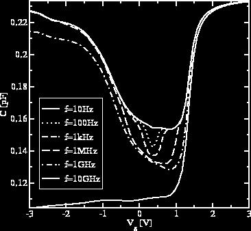
Frequency dispersion effect and parameters. extraction method for novel HfO 2 as gate dielectric
 048 SCIENCE CHINA Information Sciences April 2010 Vol. 53 No. 4: 878 884 doi: 10.1007/s11432-010-0079-8 Frequency dispersion effect and parameters extraction method for novel HfO 2 as gate dielectric LIU
Temperature dependence of spin diffusion length in silicon by Hanle-type spin. precession
 Temperature dependence of spin diffusion length in silicon by Hanle-type spin precession T. Sasaki 1,a), T. Oikawa 1, T. Suzuki 2, M. Shiraishi 3, Y. Suzuki 3, and K. Noguchi 1 SQ Research Center, TDK
TRANSVERSE SPIN TRANSPORT IN GRAPHENE
 International Journal of Modern Physics B Vol. 23, Nos. 12 & 13 (2009) 2641 2646 World Scientific Publishing Company TRANSVERSE SPIN TRANSPORT IN GRAPHENE TARIQ M. G. MOHIUDDIN, A. A. ZHUKOV, D. C. ELIAS,
Quantum and Non-local Transport Models in Crosslight Device Simulators. Copyright 2008 Crosslight Software Inc.
 Quantum and Non-local Transport Models in Crosslight Device Simulators Copyright 2008 Crosslight Software Inc. 1 Introduction Quantization effects Content Self-consistent charge-potential profile. Space
Resonant photo-ionization of point defects in HfO 2 thin films observed by second-harmonic generation.
 Optics of Surfaces & Interfaces - VIII September 10 th, 2009 Resonant photo-ionization of point defects in HfO 2 thin films observed by second-harmonic generation. Jimmy Price and Michael C. Downer Physics
Arizona State University, Tempe, AZ 85287, USA 2 Department of Electrical Engineering. Arizona State University, Tempe, AZ 85287, USA ABSTRACT
 Accurate Three-Dimensional Simulation of Electron Mobility Including Electron-Electron and Electron-Dopant Interactions C. Heitzinger, 1 C. Ringhofer, 1 S. Ahmed, 2 D. Vasileska, 2 1 Department of Mathematics
MOSFET: Introduction
 E&CE 437 Integrated VLSI Systems MOS Transistor 1 of 30 MOSFET: Introduction Metal oxide semiconductor field effect transistor (MOSFET) or MOS is widely used for implementing digital designs Its major
The Critical Role of Quantum Capacitance in Compact Modeling of Nano-Scaled and Nanoelectronic Devices
 The Critical Role of Quantum Capacitance in Compact Modeling of Nano-Scaled and Nanoelectronic Devices Zhiping Yu and Jinyu Zhang Institute of Microelectronics Tsinghua University, Beijing, China yuzhip@tsinghua.edu.cn
Future Trends in Microelectronics Impact on Detector Readout. Paul O Connor
 Future Trends in Microelectronics Impact on Detector Readout Paul O Connor Outline CMOS Technology Scaling Analog Circuits Radiation Effects Cost Detector Development Symposium Paul O'Connor BNL April
! CMOS Process Enhancements. ! Semiconductor Physics. " Band gaps. " Field Effects. ! MOS Physics. " Cut-off. " Depletion.
 ESE 570: Digital Integrated Circuits and VLSI Fundamentals Lec 4: January 3, 018 MOS Transistor Theory, MOS Model Lecture Outline! CMOS Process Enhancements! Semiconductor Physics " Band gaps " Field Effects!
Lecture 20 - Semiconductor Structures
 Lecture 0: Structures Kittel Ch 17, p 494-503, 507-511 + extra material in the class notes MOS Structure metal Layer Structure Physics 460 F 006 Lect 0 1 Outline What is a semiconductor Structure? Created
A Theoretical Investigation of Surface Roughness Scattering in Silicon Nanowire Transistors
 A Theoretical Investigation of Surface Roughness Scattering in Silicon Nanowire Transistors Jing Wang *, Eric Polizzi **, Avik Ghosh *, Supriyo Datta * and Mark Lundstrom * * School of Electrical and Computer