Nanocarbon Interconnects - From 1D to 3D
|
|
|
- Janice Short
- 5 years ago
- Views:
Transcription
1 Nanocarbon Interconnects - From 1D to 3D Cary Y. Yang Santa Clara University
2 Outline Introduction CNT as 1D interconnect structure CNT-graphene as all-carbon 3D interconnect Summary


3 Device Scaling driven by Moore s Law Doubles number of transistors on-chip every two years Enables packing more functions Reduces cost


4 On-chip Interconnects Intel 14 nm process press release 9/2014


5 Effect of Scaling on Interconnect Performance Resistivity of Cu surges with downward scaling ITRS 2007
6 Effect of Scaling on Interconnect Performance RC delay due to local interconnects IMEC, IITC 2016


7 Effect of Scaling on Interconnect Reliability Current density approaching electromigration limit of Cu interconnects Voids formed causing failure of interconnects SEM picture of an EM-failed Cu via ITRS 2013 M. A. Hussein, J. He, IEEE Trans. Semicon. Manufacturing 18 (2005)

: - Smaller grains")
, Ag (12 µω-cm) - Current capacity 10 x Cu -")

8 Alternative Interconnect Materials and Structures Conductors with electron mean free path λ either significantly larger or smaller than those in Cu and W Current-carrying capacity significantly higher than Cu and W Cu Barrier Seed Electroplated Cu Inter-level dielectric Silicides (small λ): - Smaller grains than Cu less variation in ρ with scaling, e.g., NiSi x (30 µω-cm), Ag (12 µω-cm) - Current capacity 10 x Cu - Stoichiometry control Nanocarbons (large λ): - Near-ballistic transport - Current capacity 100 x Cu - High contact resistance Cu+ Cu + BS BS Cu Long MFP large λ Small λ Small MFP Interconnect Technologist Clarke et al., VLSI 2014

 vs Cu 400 W/(K m) Contact resistance")
9 Alternative Interconnect Materials and Structures Nanocarbons as potential replacements for Cu Electromigration-resistant - Current-carrying capability > 10 7 A/cm 2 Long mean free path - High mobility and near-ballistic transport High thermal conductivity W/(K m) vs Cu 400 W/(K m) Contact resistance challenges

10 Alternative Interconnect Materials and Structures CNT vias/plugs in local interconnects M. H. Van der Veen, et al., IITC 2012


11 Alternative Interconnect Materials and Structures Graphene interconnects 8-nm-wide intercalated MLG: resistivity of 3.2 μω cm 30-nm-width bilayer interconnects of multilayer graphene and Ni D. Kondo, et al., IITC 2014 T. Ishikura, et al., IITC 2015


12 Nanocarbon Interconnects: Contact Resistance Challenges CNT-metal contacts Graphene-metal contacts P. Wilhite, et al., SST 29 (2014) Politou, et al., APL 107 (2015)

13 All-Carbon Interconnects: 1D to 3D CNT as local vertical interconnect Graphene as horizontal interconnect and/or active channel material sp 2 -bonded carbon interconnect F.D. Novaes,et al., ACS Nano (2010) Extension of superior nanocarbon properties to 3D integration sp 2 bonding for high electrical and thermal conductance
14 Outline Introduction CNT as 1D interconnect structure CNT-graphene as all-carbon 3D interconnect Summary
15 CNT Vias - Objectives Comprehensive characterization of CNT vias with linewidths approaching those used in current technology nodes Development of technique to extract contact resistance of fabricated CNT vias with linewidths down to 40 nm Assessment of CNT via performance and reliability and comparisons with Cu and W


16 Via Test Structure Fabrication Modify process to include a-si hard mask for via etching to achieve vertical sidewalls C. Zhou, et al., IEEE EDL 36, (2015)


17 Via Test Structures 200 nm CNT via patterns: layout design Wedge structure to create multiple heights
")
18 CNT Growth in Vias Vertically aligned CNTs are grown in vias using Ni catalyst in plasma-enhanced chemical vapor deposition (PECVD) system

19 Dielectric Filling and Polishing To maintain CNT vertical alignment in vias and to optimize CNT/metal interface at via top contact, void in via filled with Al 2 O 3 Atomic Layer Deposition of Al 2 O 3 using trimethylaluminum and water at a rate of 1 Å/cycle
 Pt deposited on alternate vias along the wedge for five different via")
20 Via Top Contact Metallization Selective top-contact metallization using electronbeam-induced deposition (EBID) Pt deposited on alternate vias along the wedge for five different via heights
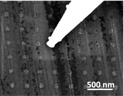
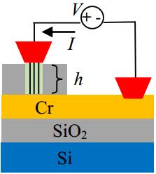
21 Electrical Characterization Nanoprobing on individual vias to measure resistance

22 Resistance of CNT Vias vs Via width Lowest resistance obtained for a 60 nm via is 150 Ω. Lowest extrapolated resistance for a 30 nm via is 295 Ω. Statistical log average of R via for 60 nm vias is 1.7 kω with standard deviation between 420 Ω and 7.1 kω. C. Zhou, et al., IEEE EDL 36, (2015)
23 Resistance of 40 nm CNT Vias vs Via Height R via = R m + R C + ρ CNT h /A CNT R m = Underlayer, probes, probe contact contribution R C = Total CNT contact resistance ρ CNT = CNT resistivity A CNT = Total area of CNTs inside via No cap EBID-Pt cap A. Vyas, et al., Nanotechnology 27, (2016)

24 CNT Via Reliability Current stress experiment carried out to determine maximum current-carrying capacity J via = 330 MA/cm 2 1mA
25 Comparisons with Cu and W Via Width Height CNT Growth Temp ( C) CNT Areal Density (#/cm 2 ) Average CNT diameter (nm) R via (kω) This Work 40 nm 80 nm CNT via (Graham 2005) 30 nm 150 nm CNT via (Katagiri 2011) 70 nm 100 nm Cu (Adelman 2014) 30 nm 130 nm NA NA NA W (Walls 1997) 30 nm 130 nm NA NA NA J via (MA/cm 2 )
26 Outline Introduction CNT as 1D interconnect structure CNT-graphene as all-carbon 3D interconnect Summary

27 CNT/Graphene Test Structure Fabrication Graphene Growth Graphene Transfer onto Oxide CNT Growth on Graphene C Zhou, et al., Nanotechnology 28, (2016)
 3 Å, (c) 5 Å, and (d) 1 nm")
28 CNT/Graphene growth Fe catalyst (a) 2 Å, (b) 3 Å, (c) 5 Å, and (d) 1 nm
29 CNT-Graphene growth Fe catalyst 1 nm Fe 5 Å Fe 3 Å Fe 2 Å Fe


30 CNT Characterization Single-Walled: Diameter 1.5 nm Double-Walled: Diameter 4.8 nm Three-Walled: Diameter 6 nm Four-Walled: Diameter 7 nm

31 CNT Characterization CNT: tip growth mode

32 CNT/Graphene Characterization CNT-on- graphene: cross-section of CNT observed

33 CNT-Graphene Interface CNT-on- graphene interface observed; graphene layers probably distorted by CNT growth process

34 Electrical Characterization ALD oxide filler to strengthen CNT forest Exposure of CNT tips for probe contact Further CNT/Graphene contact resistance extraction in progress C Zhou, et al., Nanotechnology 28, (2016)
35 Summary Fabricated CNT vias down to 40 nm wide demonstrated superior reliability and promising performance CNT/Graphene 3D test structure successfully fabricated Graphene remains intact but distorted after Fe sputtering and dewetting CNT/Graphene interface is observed using TEM, suggesting some bonding between CNT walls and graphene surface CNT/Graphene contact resistance extracted from electrical measurements First-principle calculations of CNT-Graphene model structures in progress


36 Acknowledgements Changjian Zhou Anshul Vyas, Patrick Wilhite, Richie Senegor, Zachary Baron Yihan Chen, Mansun Chan Chai Yang Phillip Wang
Carbon Nanotubes for Interconnect Applications Franz Kreupl, Andrew P. Graham, Maik Liebau, Georg S. Duesberg, Robert Seidel, Eugen Unger
 Carbon Nanotubes for Interconnect Applications Franz Kreupl, Andrew P. Graham, Maik Liebau, Georg S. Duesberg, Robert Seidel, Eugen Unger Infineon Technologies Corporate Research Munich, Germany Outline
Carbon nanotubes on graphene: Electrical and interfacial properties
 Santa Clara University Scholar Commons Electrical Engineering Senior Theses Engineering Senior Theses 6-13-2017 Carbon nanotubes on graphene: Electrical and interfacial properties Richard Senegor Santa
Carbon Nanotubes in Interconnect Applications
 Carbon Nanotubes in Interconnect Applications Page 1 What are Carbon Nanotubes? What are they good for? Why are we interested in them? - Interconnects of the future? Comparison of electrical properties
Graphene devices and integration: A primer on challenges
 Graphene devices and integration: A primer on challenges Archana Venugopal (TI) 8 Nov 2016 Acknowledgments: Luigi Colombo (TI) UT Dallas and UT Austin 1 Outline Where we are Issues o Contact resistance
Are Carbon Nanotubes the Future of VLSI Interconnections? Kaustav Banerjee and Navin Srivastava University of California, Santa Barbara
 Are Carbon Nanotubes the Future of VLSI Interconnections? Kaustav Banerjee and Navin Srivastava University of California, Santa Barbara Forms of Carbon Carbon atom can form several distinct types of valence
Nanocarbon Technology for Development of Innovative Devices
 Nanocarbon Technology for Development of Innovative Devices Shintaro Sato Daiyu Kondo Shinichi Hirose Junichi Yamaguchi Graphene, a one-atom-thick honeycomb lattice made of carbon, and a carbon nanotube,
There's Plenty of Room at the Bottom
 There's Plenty of Room at the Bottom 12/29/1959 Feynman asked why not put the entire Encyclopedia Britannica (24 volumes) on a pin head (requires atomic scale recording). He proposed to use electron microscope
Plasma Etching: Atomic Scale Surface Fidelity and 2D Materials
 1 Plasma Etching: Atomic Scale Surface Fidelity and 2D Materials Thorsten Lill, Keren J. Kanarik, Samantha Tan, Meihua Shen, Alex Yoon, Eric Hudson, Yang Pan, Jeffrey Marks, Vahid Vahedi, Richard A. Gottscho
Modeling and Performance analysis of Metallic CNT Interconnects for VLSI Applications
 IOSR Journal of Electronics and Communication Engineering (IOSR-JECE) e-issn: 2278-2834, p- ISSN: 2278-8735. Volume 4, Issue 6 (Jan. - Feb. 2013), PP 32-36 Modeling and Performance analysis of Metallic
What are Carbon Nanotubes? What are they good for? Why are we interested in them?
 Growth and Properties of Multiwalled Carbon Nanotubes What are Carbon Nanotubes? What are they good for? Why are we interested in them? - Interconnects of the future? - our vision Where do we stand - our
Recap (so far) Low-Dimensional & Boundary Effects
 Low-Dimensional & Boundary Effects") Recap (so far) Ohm s & Fourier s Laws Mobility & Thermal Conductivity Heat Capacity Wiedemann-Franz Relationship Size Effects and Breakdown of Classical Laws 1 Low-Dimensional & Boundary Effects Energy
Recap (so far) Ohm s & Fourier s Laws Mobility & Thermal Conductivity Heat Capacity Wiedemann-Franz Relationship Size Effects and Breakdown of Classical Laws 1 Low-Dimensional & Boundary Effects Energy
TCAD Modeling of Stress Impact on Performance and Reliability
 TCAD Modeling of Stress Impact on Performance and Reliability Xiaopeng Xu TCAD R&D, Synopsys March 16, 2010 SEMATECH Workshop on Stress Management for 3D ICs using Through Silicon Vias 1 Outline Introduction
New Material Design and Device Simulation Tool. Dr. Gong Kui HZWTECH
 New Material Design and Device Simulation Tool Dr. Gong Kui HZWTECH 鸿之微科技 ( 上海 ) 股份有限公司 HONGZHIWEI TECHNOLOGY(SHANGHAI) CO.,LTD outline Atomistic-TCAD:new devices simulation tool Applications of Atomistic-TCAD
Research Challenges and Opportunities. in 3D Integrated Circuits. Jan 30, 2009
 Jan 3, 29 Research Challenges and Opportunities in 3D Integrated Circuits Ankur Jain ankur.jain@freescale.com, ankurjain@stanfordalumni.org Freescale Semiconductor, Inc. 28. 1 What is Three-dimensional
Graphene for future VLSI
 Graphene for future VLSI greg.yeric@arm.com Fellow ARM Research Why did the semiconductor industry get so excited about graphene? 2 The problem with planar MOSFETs Gate Source Drain Substrate One-dimensional
Temperature dependence of carbon nanofiber resistance [Nanotechnology 21, (2010)]
![Temperature dependence of carbon nanofiber resistance [Nanotechnology 21, (2010)]](/thumbs/81/84247750.jpg "Temperature dependence of carbon nanofiber resistance [Nanotechnology 21, (2010)]") Temperature dependence of carbon nanofiber resistance [Nanotechnology 21, 265707 (2010)] Toshishige Yamada *, Hisashi Yabutani, Tsutomu Saito, and Cary Y. Yang Center for Nanostructures, Santa Clara University,
Temperature dependence of carbon nanofiber resistance [Nanotechnology 21, 265707 (2010)] Toshishige Yamada *, Hisashi Yabutani, Tsutomu Saito, and Cary Y. Yang Center for Nanostructures, Santa Clara University,
Elementary Process of Electromigration at Metallic Nanojunctions in the Ballistic Regime
 Elementary Process of Electromigration at Metallic Nanojunctions in the Ballistic Regime Kaz Hirakawa Institute of Industrial Science, University of Tokyo CREST, JST collaborators: Akinori Umeno, Kenji
Thermal Conductivity of Carbon Nanotube Composite Films
 Mat. Res. Soc. Symp. Proc. Vol. 812 2004 Materials Research Society F3.18.1 Thermal Conductivity of Carbon Nanotube Composite Films Quoc Ngo 1,2, Brett A. Cruden 2, Alan M. Cassell 2, Megan D. Walker 2,
Chapter 3 Engineering Science for Microsystems Design and Fabrication
 Lectures on MEMS and MICROSYSTEMS DESIGN and MANUFACTURE Chapter 3 Engineering Science for Microsystems Design and Fabrication In this Chapter, we will present overviews of the principles of physical and
Alternative deposition solution for cost reduction of TSV integration
 Alternative deposition solution for cost reduction of TSV integration J. Vitiello, F. Piallat, L. Bonnet KOBUS 611 rue Aristide Bergès, Z.A. de Pré Millet, Montbonnot-Saint-Martin, 38330 France Ph: +33
Manufacture of Nanostructures for Power Electronics Applications
 Manufacture of Nanostructures for Power Electronics Applications Brian Hunt and Jon Lai Etamota Corporation 2672 E. Walnut St. Pasadena, CA 91107 APEC, Palm Springs Feb. 23rd, 2010 1 Background Outline
ECE520 VLSI Design. Lecture 8: Interconnect Manufacturing and Modeling. Payman Zarkesh-Ha
 ECE520 VLSI Design Lecture 8: Interconnect Manufacturing and Modeling Payman Zarkesh-Ha Office: ECE Bldg. 230B Office hours: Wednesday 2:00-3:00PM or by appointment E-mail: pzarkesh@unm.edu Slide: 1 Review
Carbon Nanomaterials: Nanotubes and Nanobuds and Graphene towards new products 2030
 Carbon Nanomaterials: Nanotubes and Nanobuds and Graphene towards new products 2030 Prof. Dr. Esko I. Kauppinen Helsinki University of Technology (TKK) Espoo, Finland Forecast Seminar February 13, 2009
Introduction to Nanotechnology Chapter 5 Carbon Nanostructures Lecture 1
 Introduction to Nanotechnology Chapter 5 Carbon Nanostructures Lecture 1 ChiiDong Chen Institute of Physics, Academia Sinica chiidong@phys.sinica.edu.tw 02 27896766 Carbon contains 6 electrons: (1s) 2,
Graphene Novel Material for Nanoelectronics
 Graphene Novel Material for Nanoelectronics Shintaro Sato Naoki Harada Daiyu Kondo Mari Ohfuchi (Manuscript received May 12, 2009) Graphene is a flat monolayer of carbon atoms with a two-dimensional honeycomb
EE410 vs. Advanced CMOS Structures
 EE410 vs. Advanced CMOS Structures Prof. Krishna S Department of Electrical Engineering S 1 EE410 CMOS Structure P + poly-si N + poly-si Al/Si alloy LPCVD PSG P + P + N + N + PMOS N-substrate NMOS P-well
nmos IC Design Report Module: EEE 112
 nmos IC Design Report Author: 1302509 Zhao Ruimin Module: EEE 112 Lecturer: Date: Dr.Zhao Ce Zhou June/5/2015 Abstract This lab intended to train the experimental skills of the layout designing of the
Thermal-reliable 3D Clock-tree Synthesis Considering Nonlinear Electrical-thermal-coupled TSV Model
 Thermal-reliable 3D Clock-tree Synthesis Considering Nonlinear Electrical-thermal-coupled TSV Model Yang Shang 1, Chun Zhang 1, Hao Yu 1, Chuan Seng Tan 1, Xin Zhao 2, Sung Kyu Lim 2 1 School of Electrical
Chapter 12: Electrical Properties. RA l
 Charge carriers and conduction: Chapter 12: Electrical Properties Charge carriers include all species capable of transporting electrical charge, including electrons, ions, and electron holes. The latter
Film Deposition Part 1
 1 Film Deposition Part 1 Chapter 11 : Semiconductor Manufacturing Technology by M. Quirk & J. Serda Spring Semester 2013 Saroj Kumar Patra Semidonductor Manufacturing Technology, Norwegian University of
Hybrid Wafer Level Bonding for 3D IC
 Hybrid Wafer Level Bonding for 3D IC An Equipment Perspective Markus Wimplinger, Corporate Technology Development & IP Director History & Roadmap - BSI CIS Devices???? 2013 2 nd Generation 3D BSI CIS with
Plasma Deposition (Overview) Lecture 1
 Lecture 1") Plasma Deposition (Overview) Lecture 1 Material Processes Plasma Processing Plasma-assisted Deposition Implantation Surface Modification Development of Plasma-based processing Microelectronics needs (fabrication
Plasma Deposition (Overview) Lecture 1 Material Processes Plasma Processing Plasma-assisted Deposition Implantation Surface Modification Development of Plasma-based processing Microelectronics needs (fabrication
Supporting Online Material for
 www.sciencemag.org/cgi/content/full/327/5966/662/dc Supporting Online Material for 00-GHz Transistors from Wafer-Scale Epitaxial Graphene Y.-M. Lin,* C. Dimitrakopoulos, K. A. Jenkins, D. B. Farmer, H.-Y.
Intrinsic Electronic Transport Properties of High. Information
 Intrinsic Electronic Transport Properties of High Quality and MoS 2 : Supporting Information Britton W. H. Baugher, Hugh O. H. Churchill, Yafang Yang, and Pablo Jarillo-Herrero Department of Physics, Massachusetts
Performance Analysis of Multilayer Graphene Nano Ribbon as on chip Interconnect.
 Performance Analysis of Multilayer Graphene Nano Ribbon as on chip Interconnect. G.Chitra 1, P.Murugeswari 2 1 (Post Graduate Student, VLSI Design, Theni Kammavar Sangam College of Technology, Theni, India)
EECS240 Spring Today s Lecture. Lecture 2: CMOS Technology and Passive Devices. Lingkai Kong EECS. EE240 CMOS Technology
 EECS240 Spring 2013 Lecture 2: CMOS Technology and Passive Devices Lingkai Kong EECS Today s Lecture EE240 CMOS Technology Passive devices Motivation Resistors Capacitors (Inductors) Next time: MOS transistor
IC Fabrication Technology
 IC Fabrication Technology * History: 1958-59: J. Kilby, Texas Instruments and R. Noyce, Fairchild * Key Idea: batch fabrication of electronic circuits n entire circuit, say 10 7 transistors and 5 levels
Fabrication Technology, Part I
 EEL5225: Principles of MEMS Transducers (Fall 2004) Fabrication Technology, Part I Agenda: Microfabrication Overview Basic semiconductor devices Materials Key processes Oxidation Thin-film Deposition Reading:
EE143 LAB. Professor N Cheung, U.C. Berkeley
 EE143 LAB 1 1 EE143 Equipment in Cory 218 2 Guidelines for Process Integration * A sequence of Additive and Subtractive steps with lateral patterning Processing Steps Si wafer Watch out for materials compatibility
Lecture 15: Scaling & Economics
 Lecture 15: Scaling & Economics Outline Scaling Transistors Interconnect Future Challenges Economics 2 Moore s Law Recall that Moore s Law has been driving CMOS [Moore65] Corollary: clock speeds have improved
Exceptional ballistic transport in epigraphene. Walt de Heer Georgia Institute of Technology
 Exceptional ballistic transport in epigraphene Walt de Heer Georgia Institute of Technology Program Objective First formulated in 2001 and patented in 2003, our objective is to develop nanoelectronics
Metallic: 2n 1. +n 2. =3q Armchair structure always metallic = 2
 Properties of CNT d = 2.46 n 2 2 1 + n1n2 + n2 2π Metallic: 2n 1 +n 2 =3q Armchair structure always metallic a) Graphite Valence(π) and Conduction(π*) states touch at six points(fermi points) Carbon Nanotube:
Asymmetrical heating behavior of doped Si channels in bulk silicon and in silicon-on-insulator under high current stress
 JOURNAL OF APPLIED PHYSICS VOLUME 86, NUMBER 12 15 DECEMBER 1999 Asymmetrical heating behavior of doped Si channels in bulk silicon and in silicon-on-insulator under high current stress C. N. Liao, a)
3/10/2013. Lecture #1. How small is Nano? (A movie) What is Nanotechnology? What is Nanoelectronics? What are Emerging Devices?
 What is Nanotechnology? What is Nanoelectronics? What are Emerging Devices?") EECS 498/598: Nanocircuits and Nanoarchitectures Lecture 1: Introduction to Nanotelectronic Devices (Sept. 5) Lectures 2: ITRS Nanoelectronics Road Map (Sept 7) Lecture 3: Nanodevices; Guest Lecture by
EECS 498/598: Nanocircuits and Nanoarchitectures Lecture 1: Introduction to Nanotelectronic Devices (Sept. 5) Lectures 2: ITRS Nanoelectronics Road Map (Sept 7) Lecture 3: Nanodevices; Guest Lecture by
Nanostrukturphysik (Nanostructure Physics)
") Nanostrukturphysik (Nanostructure Physics) Prof. Yong Lei & Dr. Yang Xu Fachgebiet 3D-Nanostrukturierung, Institut für Physik Contact: yong.lei@tu-ilmenau.de; yang.xu@tu-ilmenau.de Office: Unterpoerlitzer
Nanostrukturphysik (Nanostructure Physics) Prof. Yong Lei & Dr. Yang Xu Fachgebiet 3D-Nanostrukturierung, Institut für Physik Contact: yong.lei@tu-ilmenau.de; yang.xu@tu-ilmenau.de Office: Unterpoerlitzer
SWCNT Based Interconnect Modeling Using Verilog-AMS
 SW Based Interconnect odeling Using Verilog-AS Hafizur Rahaman, Debaprasad Das*, and Avishek Sinha Roy** School of VSI Technology, Bengal Engineering and Science University, Shibpur, India. Email: rahaman_h@it.becs.ac.in,
Wafer-scale fabrication of graphene
 Wafer-scale fabrication of graphene Sten Vollebregt, MSc Delft University of Technology, Delft Institute of Mircosystems and Nanotechnology Delft University of Technology Challenge the future Delft University
Supporting Information. Fast Synthesis of High-Performance Graphene by Rapid Thermal Chemical Vapor Deposition
 1 Supporting Information Fast Synthesis of High-Performance Graphene by Rapid Thermal Chemical Vapor Deposition Jaechul Ryu, 1,2, Youngsoo Kim, 4, Dongkwan Won, 1 Nayoung Kim, 1 Jin Sung Park, 1 Eun-Kyu
EE 292L : Nanomanufacturing. Week 5: Advanced Process Technology. Oct
 EE 292L : Nanomanufacturing Week 5: Advanced Process Technology Oct 22 2012 1 Advanced Process Technology 1 HAR etch 2 3 HAR Gapfill Metal ALD 4 Reflow 5 6 SAC Airgap 7 8 Strain Ge/III-V Engineering 1
N ano scale l S il ii lco i n B ased N o nvo lat l i atl ie l M em ory r Chungwoo Kim, Ph.D.
 cw_kim@samsung.com Acknowledgements Collaboration Funding Outline Introduction Current research status Nano fabrication Process Nanoscale patterning SiN thin film Si Nanoparticle Nano devices Nanoscale
Self-study problems and questions Processing and Device Technology, FFF110/FYSD13
 Self-study problems and questions Processing and Device Technology, FFF110/FYSD13 Version 2016_01 In addition to the problems discussed at the seminars and at the lectures, you can use this set of problems
EV Group. Engineered Substrates for future compound semiconductor devices
 EV Group Engineered Substrates for future compound semiconductor devices Engineered Substrates HB-LED: Engineered growth substrates GaN / GaP layer transfer Mobility enhancement solutions: III-Vs to silicon
CMOS Scaling. Two motivations to scale down. Faster transistors, both digital and analog. To pack more functionality per area. Lower the cost!
 Two motivations to scale down CMOS Scaling Faster transistors, both digital and analog To pack more functionality per area. Lower the cost! (which makes (some) physical sense) Scale all dimensions and
TEMPERATURE DEPENDENT ANALYSIS OF MIXED CARBON NANOTUBE BUNDLE AS VLSI INTERCONNECTS MASTER OF TECHNOLOGY IN VLSI DESIGN
 TEMPERATURE DEPENDENT ANALYSIS OF MIXED CARBON NANOTUBE BUNDLE AS VLSI INTERCONNECTS Thesis submitted in the partial fulfillment of the requirement for the award of degree of MASTER OF TECHNOLOGY IN VLSI
EE130: Integrated Circuit Devices
 EE130: Integrated Circuit Devices (online at http://webcast.berkeley.edu) Instructor: Prof. Tsu-Jae King (tking@eecs.berkeley.edu) TA s: Marie Eyoum (meyoum@eecs.berkeley.edu) Alvaro Padilla (apadilla@eecs.berkeley.edu)
SUPPLEMENTARY INFORMATION
 doi:.38/nature09979 I. Graphene material growth and transistor fabrication Top-gated graphene RF transistors were fabricated based on chemical vapor deposition (CVD) grown graphene on copper (Cu). Cu foil
Scaling up Chemical Vapor Deposition Graphene to 300 mm Si substrates
 Scaling up Chemical Vapor Deposition Graphene to 300 mm Si substrates Co- Authors Aixtron Alex Jouvray Simon Buttress Gavin Dodge Ken Teo The work shown here has received partial funding from the European
Effects of Current Spreading on the Performance of GaN-Based Light-Emitting Diodes
 IEEE TRANSACTIONS ON ELECTRON DEVICES, VOL. 48, NO. 6, JUNE 2001 1065 Effects of Current Spreading on the Performance of GaN-Based Light-Emitting Diodes Hyunsoo Kim, Seong-Ju Park, and Hyunsang Hwang Abstract
Transmission Electron Microscopy for metrology and characterization of semiconductor devices
 Transmission Electron Microscopy for metrology and characterization of semiconductor devices Bert Freitag, Laurens Kwakman, Ivan Lazic and Frank de Jong FEI / ThermoFisher Scientific, Achtseweg Noord 5,
Wafer Charging in Process Equipment and its Relationship to GMR Heads Charging Damage
 Wafer Charging in Process Equipment and its Relationship to GMR Heads Charging Damage Wes Lukaszek Wafer Charging Monitors, Inc. 127 Marine Road, Woodside, CA 94062 tel.: (650) 851-9313, fax.: (650) 851-2252,
Transport through Andreev Bound States in a Superconductor-Quantum Dot-Graphene System
 Transport through Andreev Bound States in a Superconductor-Quantum Dot-Graphene System Nadya Mason Travis Dirk, Yung-Fu Chen, Cesar Chialvo Taylor Hughes, Siddhartha Lal, Bruno Uchoa Paul Goldbart University
Taurus-Topography. Topography Modeling for IC Technology
 SYSTEMS PRODUCTS LOGICAL PRODUCTS PHYSICAL IMPLEMENTATION SIMULATION AND ANALYSIS LIBRARIES TCAD Aurora DFM WorkBench Davinci Medici Raphael Raphael-NES Silicon Early Access TSUPREM-4 Taurus-Device Taurus-Lithography
Fabrication at the nanoscale for nanophotonics
 Fabrication at the nanoscale for nanophotonics Ilya Sychugov, KTH Materials Physics, Kista silicon nanocrystal by electron beam induced deposition lithography Outline of basic nanofabrication methods Devices
M R S Internet Journal of Nitride Semiconductor Research
 Page 1 of 6 M R S Internet Journal of Nitride Semiconductor Research Volume 9, Article 7 The Ambient Temperature Effect on Current-Voltage Characteristics of Surface-Passivated GaN-Based Field-Effect Transistors
Graphene The Search For Two Dimensions. Christopher Scott Friedline Arizona State University
 Graphene The Search For Two Dimensions Christopher Scott Friedline Arizona State University What Is Graphene? Single atomic layer of graphite arranged in a honeycomb crystal lattice Consists of sp 2 -bonded
Simulation of Ion Beam Etching of Patterned Nanometer-scale Magnetic Structures for High-Density Storage Applications
 Engineered Excellence A Journal for Process and Device Engineers Simulation of Ion Beam Etching of Patterned Nanometer-scale Magnetic Structures for High-Density Storage Applications Introduction Fabrication
MOS Transistor Properties Review
 MOS Transistor Properties Review 1 VLSI Chip Manufacturing Process Photolithography: transfer of mask patterns to the chip Diffusion or ion implantation: selective doping of Si substrate Oxidation: SiO
Fig The electron mobility for a-si and poly-si TFT.
 Fig. 1-1-1 The electron mobility for a-si and poly-si TFT. Fig. 1-1-2 The aperture ratio for a-si and poly-si TFT. 33 Fig. 1-2-1 All kinds defect well. (a) is the Dirac well. (b) is the repulsive Columbic
Reliability of TSV interconnects in 3D-IC
 Reliability of interconnects in 3D-IC Electromigration voiding analyzed through 3D-FIB-SEM T. Frank, C. Chappaz, F. Lorut - STMicroelectronics, Crolles, France P. Leduc, L. Arnaud, S. Moreau, A. Thuaire
Molecular Electronics For Fun and Profit(?)
") Molecular Electronics For Fun and Profit(?) Prof. Geoffrey Hutchison Department of Chemistry University of Pittsburgh geoffh@pitt.edu July 22, 2009 http://hutchison.chem.pitt.edu Moore s Law: Transistor
Molecular Electronics For Fun and Profit(?) Prof. Geoffrey Hutchison Department of Chemistry University of Pittsburgh geoffh@pitt.edu July 22, 2009 http://hutchison.chem.pitt.edu Moore s Law: Transistor
Equivalent Circuit Model Extraction for Interconnects in 3D ICs
 Equivalent Circuit Model Extraction for Interconnects in 3D ICs A. Ege Engin Assistant Professor, Department of ECE, San Diego State University Email: aengin@mail.sdsu.edu ASP-DAC, Jan. 23, 213 Outline
Auger Electron Spectroscopy Overview
 Auger Electron Spectroscopy Overview Also known as: AES, Auger, SAM 1 Auger Electron Spectroscopy E KLL = E K - E L - E L AES Spectra of Cu EdN(E)/dE Auger Electron E N(E) x 5 E KLL Cu MNN Cu LMM E f E
Lecture #39. Transistor Scaling
 Lecture #39 ANNOUNCEMENT Pick up graded HW assignments and exams (78 Cory) Lecture #40 will be the last formal lecture. Class on Friday will be dedicated to a course review (with sample problems). Discussion
Stretching the Barriers An analysis of MOSFET Scaling. Presenters (in order) Zeinab Mousavi Stephanie Teich-McGoldrick Aseem Jain Jaspreet Wadhwa
 Zeinab Mousavi Stephanie Teich-McGoldrick Aseem Jain Jaspreet Wadhwa") Stretching the Barriers An analysis of MOSFET Scaling Presenters (in order) Zeinab Mousavi Stephanie Teich-McGoldrick Aseem Jain Jaspreet Wadhwa Why Small? Higher Current Lower Gate Capacitance Higher
Stretching the Barriers An analysis of MOSFET Scaling Presenters (in order) Zeinab Mousavi Stephanie Teich-McGoldrick Aseem Jain Jaspreet Wadhwa Why Small? Higher Current Lower Gate Capacitance Higher
Multilayer Wiring Technology with Grinding Planarization of Dielectric Layer and Via Posts
 Tani et al.: Multilayer Wiring Technology with Grinding Planarization (1/6) [Technical Paper] Multilayer Wiring Technology with Grinding Planarization of Dielectric Layer and Via Posts Motoaki Tani, Kanae
COMPARATIVE ANALYSIS OF CARBON NANOTUBES AS VLSI INTERCONNECTS
 International Journal of Science, Engineering and Technology Research (IJSETR), Volume 4, Issue 8, August 15 COMPARATIVE ANALYSIS OF CARBON NANOTUBES AS VLSI INTERCONNECTS Priya Srivastav, Asst. Prof.
Emerging spintronics-based logic technologies
 Center for Spintronic Materials, Interfaces, and Novel Architectures Emerging spintronics-based logic technologies Zhaoxin Liang Meghna Mankalale Jian-Ping Wang Sachin S. Sapatnekar University of Minnesota
SUPPLEMENTARY INFORMATION
 doi:10.1038/nature17653 Supplementary Methods Electronic transport mechanism in H-SNO In pristine RNO, pronounced electron-phonon interaction results in polaron formation that dominates the electronic
GHZ ELECTRICAL PROPERTIES OF CARBON NANOTUBES ON SILICON DIOXIDE MICRO BRIDGES
 GHZ ELECTRICAL PROPERTIES OF CARBON NANOTUBES ON SILICON DIOXIDE MICRO BRIDGES SHENG F. YEN 1, HAROON LAIS 1, ZHEN YU 1, SHENGDONG LI 1, WILLIAM C. TANG 1,2, AND PETER J. BURKE 1,2 1 Electrical Engineering
SUPPLEMENTARY NOTES Supplementary Note 1: Fabrication of Scanning Thermal Microscopy Probes
 SUPPLEMENTARY NOTES Supplementary Note 1: Fabrication of Scanning Thermal Microscopy Probes Fabrication of the scanning thermal microscopy (SThM) probes is summarized in Supplementary Fig. 1 and proceeds
ALD-enabled nanopatterning: area-selective ALD by area-activation
 ALD-enabled nanopatterning: area-selective ALD by area-activation Adrie Mackus, Ageeth Bol, and Erwin Kessels w.m.m.kessels@tue.nl www.tue.nl/pmp Outline Introduction & Area-selective deposition Area-selective
Carbon Nanotube Interconnect: Challenges and Solutions for On-Chip Communication in Future Nanoscale ICs
 Carbon Nanotube Interconnect: Challenges and Solutions for On-Chip Communication in Future Nanoscale ICs Arthur Nieuwoudt ELEC 527 Presentation Rice University 3/13/2007 Copyright 2007 by Arthur Nieuwoudt.
Are Carbon Nanotubes the Future of VLSI Interconnections?
 Are Carbon Nanotubes the Future of VLSI Interconnections? Kaustav Banerjee and Navin Srivastava Electrical and Computer Engineering, University of California, Santa Barbara, CA 93106 e-mail: {kaustav,
Introduction to Nanotechnology Chapter 5 Carbon Nanostructures Lecture 1
 Introduction to Nanotechnology Chapter 5 Carbon Nanostructures Lecture 1 ChiiDong Chen Institute of Physics, Academia Sinica chiidong@phys.sinica.edu.tw 02 27896766 Section 5.2.1 Nature of the Carbon Bond
Ultralow-Power Reconfigurable Computing with Complementary Nano-Electromechanical Carbon Nanotube Switches
 Ultralow-Power Reconfigurable Computing with Complementary Nano-Electromechanical Carbon Nanotube Switches Presenter: Tulika Mitra Swarup Bhunia, Massood Tabib-Azar, and Daniel Saab Electrical Eng. And
Carbon nanotubes as vertical interconnects in 3D integrated circuits
 Carbon nanotubes as vertical interconnects in 3D integrated circuits Masters Thesis by Sten Vollebregt born on the 15th of May 1984 in Delft September 5, 2009 Supervisors: Prof. dr. C.I.M. Beenakker Dr.
Low Contact Resistance on p-sige Junctions with B / Ga Implants and Nanosecond Laser Anneal
 Low Contact Resistance on p-sige Junctions with B / Ga Implants and Nanosecond Laser Anneal Fareen Adeni Khaja Technical Product Marketing, Front End Products Transistor and Interconnect Group Applied
Paper and Cellulosic Materials as Flexible Substrates for 2D Electronic Materials
 Paper and Cellulosic Materials as Flexible Substrates for 2D Electronic Materials Prof. Eric M. Vogel, Prof. M. Shofner, Brian Beatty Materials Science & Engineering Trends in Electronics Internet of things
A Mechanical Model for Erosion in Copper Chemical-Mechanical Polishing
 A Mechanical Model for Erosion in Copper Chemical-Mechanical Polishing Kyungyoon Noh, Nannaji Saka and Jung-Hoon Chun Laboratory for Manufacturing and Productivity Massachusetts Institute of Technology
Enhanced performance of microbolometer. using coupled feed horn antenna
 Enhanced performance of microbolometer using coupled feed horn antenna Kuntae Kim*,a, Jong-Yeon Park*, Ho-Kwan Kang*, Jong-oh Park*, Sung Moon*, Jung-ho Park a * Korea Institute of Science and Technology,
Design and Fabrication of Microheaters for Localized Carbon Nanotube Growth
 Design and Fabrication of Microheaters for Localized Carbon Nanotube Growth Y. Zhou 1, J. Johnson 1, L. Wu 1, S. Maley 2, A. Ural 1, and H. Xie 1 1 Department of Electrical and Computer Engineering, University
SUPPORTING INFORMATION: Titanium Contacts to Graphene: Process-Induced Variability in Electronic and Thermal Transport
 SUPPORTING INFORMATION: Titanium Contacts to Graphene: Process-Induced Variability in Electronic and Thermal Transport Keren M. Freedy 1, Ashutosh Giri 2, Brian M. Foley 2, Matthew R. Barone 1, Patrick
Diameter Optimization for Highest Degree of Ballisticity of Carbon Nanotube Field Effect Transistors I. Khan, O. Morshed and S. M.
 Diameter Optimization for Highest Degree of Ballisticity of Carbon Nanotube Field Effect Transistors I. Khan, O. Morshed and S. M. Mominuzzaman Department of Electrical and Electronic Engineering, Bangladesh
Supplementary Information
 Supplementary Information Supplementary Figure 1. fabrication. A schematic of the experimental setup used for graphene Supplementary Figure 2. Emission spectrum of the plasma: Negative peaks indicate an
Lecture 0: Introduction
 Lecture 0: Introduction Introduction q Integrated circuits: many transistors on one chip q Very Large Scale Integration (VLSI): bucketloads! q Complementary Metal Oxide Semiconductor Fast, cheap, low power
MODELING RELIABILITY IN COPPER/LOW-K INTERCONNECTS AND VARIABILITY IN CMOS
 MODELING RELIABILITY IN COPPER/LOW-K INTERCONNECTS AND VARIABILITY IN CMOS A Dissertation Presented to The Academic Faculty by Muhammad Muqarrab Bashir In Partial Fulfillment of the Requirements for the
2D Materials for Gas Sensing
 2D Materials for Gas Sensing S. Guo, A. Rani, and M.E. Zaghloul Department of Electrical and Computer Engineering The George Washington University, Washington DC 20052 Outline Background Structures of
Supplementary Figure S1. AFM images of GraNRs grown with standard growth process. Each of these pictures show GraNRs prepared independently,
 Supplementary Figure S1. AFM images of GraNRs grown with standard growth process. Each of these pictures show GraNRs prepared independently, suggesting that the results is reproducible. Supplementary Figure
Thin Wafer Handling Debonding Mechanisms
 Thin Wafer Handling Debonding Mechanisms Jonathan Jeauneau, Applications Manager Alvin Lee, Technology Strategist Dongshun Bai, Scientist, 3-D IC R&D Materials Outline Requirements of Thin Wafer Handling
Low Power Phase Change Memory via Block Copolymer Self-assembly Technology
 Low Power Phase Change Memory via Block Copolymer Self-assembly Technology Beom Ho Mun 1, Woon Ik Park 1, You Yin 2, Byoung Kuk You 1, Jae Jin Yun 1, Kung Ho Kim 1, Yeon Sik Jung 1*, and Keon Jae Lee 1*