The effect of point defects in zircon
|
|
|
- Shanon French
- 5 years ago
- Views:
Transcription
1 aterials for nuclear waste immobilization: The effect of point defects in zircon iguel Pruneda Department of Earth Sciences University of Centre for Ceramic Immobilisation
2 Radiation damage process α-decay process α-particle ~ 5 ev Recoil ~ 100 kev 238 U / 234 Th l It causes: Amorphisation (metamict) Swelling Cracks Leaching Zircon: model study: old natural samples


3 Why first principles? Atomistic description Complex structures D simulations Empirical potentials Complex chemistry Zr, Ti, Sn, Ca, La, Gd,

4 Swelling in zircon (ZrSiO 4 ) X-Rays Crystalline swelling: lattice parameters vs dose Total: ~20% Crystalline: ~5% anisotropic
5 IR, Raman and NR spectroscopies IR NR I. Farnan & E.K.H Salje, JAP 89, 2084 (2001). Zhang & E. K. H Salje, J. Phys. Condens. atter 13, 3057 (2001)
 SiO4 tetrahedra remain essentially undistorted Larger anisotropic displacement parameters found for Zr and O atoms DFT calculations: Formation energies for a choice of chemical")
6 Localized defects in radiation-damaged zircon (Rios et. al. Acta Cryst. (2000) B56, 947) X-ray diffraction experiments in natural samples. (1.8x10 18 α-decay/g) SiO4 tetrahedra remain essentially undistorted Larger anisotropic displacement parameters found for Zr and O atoms DFT calculations: Formation energies for a choice of chemical potentials High values of the formation energies for all defects, except oxygen interstitial J.-P. Crocombette, Phys. Chem. inerals 27, 138 (1999)
 DFT (LDA, GGA) Pseudopotentials (norm conserving, factorised) Numerical atomic orbitals as basis (finite range) Numerical evaluation of matrix elements (3D grid) Implemented in the SIESTA")
7 Our method Linear-scaling DFT based on NAOs (Numerical Atomic Orbitals) P. Ordejon, E. Artacho & J.. Soler, Phys. Rev. B 53, R10441 (1996) Born-Oppenheimer (relaxations, mol. dynamics) DFT (LDA, GGA) Pseudopotentials (norm conserving, factorised) Numerical atomic orbitals as basis (finite range) Numerical evaluation of matrix elements (3D grid) Implemented in the SIESTA program D. Sanchez-Portal, P. Ordejon, E. Artacho & J.. Soler Int. J. Quantum Chem. 65, 453 (1997)

8 Intrinsic point defects and volume swelling in ZrSiO 4 Radiation cascades & defect accumulation ~10 21 defects/cm 3 Si 0.2% swelling!! Tetragonal I4 1 /amd space group BCC unit cell with four formula units. Structural parameters: a, c, u, v Alternating SiO 4 tetrahedra & ZrO 8 dodecadeltahedra
9 Playing with the concentration of defects Supercell approach: n n n x Repetitions of the unit cell y z (Periodic super-structure of defects) 1x1x1 1x1x2 2x2x1 2x2x2 (24 atoms) (48 atoms) (96 atoms) (192 atoms) Lattice relaxation Low-concentration limit atomic relaxation only!
10 The catalogue of defects Interstitials: O i, Si i, Zr i Vacancies: V O, V si, V Zr Antisite defects: Zr Si & Si Zr Frenkel pairs: O FP, Si FP & Zr FP Different charge-states: 4, 3, 2, 1 + 1, + 2, + 3, + 4 0

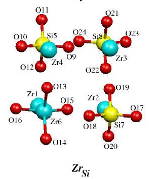
11 J.. Pruneda, T. Archer, and E. Artacho to be published in PRB Possible defects: O & Si interstitials Zr Si anti-site
12 Swelling as a function of the concentration Almost linear behavior Considerable anisotropy Effect of disorder

13 Oxygen interstitial Neutral defect has a dumbbell structure similar to ZrO2.

 743 cm")
14 Silicon interstitial Zr Si anti-site Local Vibrational odes IR active at 729 cm -1 (O i ) 743 cm -1 (Si i )
15 Simulation of NR spectra Combining methods: SIESTA+PARATEC Experiments in damaged samples Chemical shifts due to swelling?
")
")
16 O: (-170) Si: (-81.5)
17 Formation Energies f ( α q) = E( α, q) µ n q( µ E ) E + +, i i e V i µ Zr ( ) + µ Si + 4µ O = G f ZrSiO 4 µ µ Zr Si ( ) + 2µ O G f ZrO 2 ( ) + 2µ O G f SiO 2
18 The stability triangle
19 Formation energies for neutral defects Converged in size Values given at the point A ore stable defects: Vacancies and interstitials of O Antisites.
20 Properties of charged defects Negative-U behavior Gain in energy when a second electron/hole is captured Oi Oi + Oi V O VO + VO Strong ionic interaction for cation-defects (& charged FP) X 0 i + V 0 X X n i + V n+ X
 To reduce the gate leakage current: 1. the dielectric must be physically thick 2.")
21 Alternative gate dielectrics OSFET Device current drive is proportional to the oxide capacitance per unit area; thus, the best way to increase the drive current and thereby achieve high performance is to reduce the equivalent oxide thickness (EOT) To reduce the gate leakage current: 1. the dielectric must be physically thick 2. it must have reasonably large band offsets to Si Scaling of the gate-oxide thickness: Roadmaps vs. actual trends.
 Vertically scaled OSFET gate stacks and junctions: How far are we likely to go?")

22 Dielectric Constants of Zr Silicates Vol. 46, 2/3, 2002 G.. Rignanese, et. al. PRL 89, (2002) Vertically scaled OSFET gate stacks and junctions: How far are we likely to go? aterials such as HfO 2 and ZrO 2, having dielectric constants of about 15 and offsets of about 1.5 ev, have the potential of meeting the long-term leakage requirements. Their silicates have almost the same barrier height, nearly as high a dielectric constant, potentially lower charge levels, and much better thermal stability; thus, they may be even better candidates.
23 Band-Offsets In the interface, it is required a high tunneling barrier to both electrons and holes. R. Puthenkovilakam et. al. PRB (2004) Band alignment at ZrSiO4(001)/Si(100) interface. (No Zr d states in the gap)


24 Charged defects!! The dielectric cannot contain traps that would promote trapassisted tunneling or locally uncompensated charges that would degrade channel mobility. The conduction in the dielectric must be purely electronic, not ionic, and preferably by electrons only. O i O i -2
![Transition Energies E α ( q / q ) = [ E ( α, q) E ( α, q )] ( q q) f f Acceptor levels for O i,v Si and V Zr that](/docs-images/82/86442942/images/25-0.jpg "can trap electrons from the bottom of the silicon valence band.")
25 Transition Energies E α ( q / q ) = [ E ( α, q) E ( α, q )] ( q q) f f Acceptor levels for O i,v Si and V Zr that can trap electrons from the bottom of the silicon valence band. Donor level of V O can trap holes injected from silicon.
26 Conclusions We have studied the effect of high concentration of point defects in ZrSiO4. A roughly linear dependence between swelling and the defect concentration of periodically repeated defects was obtained. Based on experimental evidence of anisotropic lattice expansion, we have selected a set of defects as good candidates to be responsible of the swelling: O i, Si i, and Zr Si. Interstitials and vacancies of oxygen, and the antisite Zr Si are the most stable defects. There is a strong tendency towards ionization, and a negative-u behavior is observed.
27 Thanks to Emilio Artacho, T. D. Archer, Kostya Trachenko, artin Dove, Ian Farnan, Laurent Le Polles, Sharon Ashbrook, Jonathan Yates, Greg Lumpkin, Susana Rios, ing Zhang
Defects in Semiconductors
 Defects in Semiconductors Mater. Res. Soc. Symp. Proc. Vol. 1370 2011 Materials Research Society DOI: 10.1557/opl.2011. 771 Electronic Structure of O-vacancy in High-k Dielectrics and Oxide Semiconductors
Resonant photo-ionization of point defects in HfO 2 thin films observed by second-harmonic generation.
 Optics of Surfaces & Interfaces - VIII September 10 th, 2009 Resonant photo-ionization of point defects in HfO 2 thin films observed by second-harmonic generation. Jimmy Price and Michael C. Downer Physics
Foster, Adam; Lopez Gejo, F.; Shluger, A. L.; Nieminen, Risto Vacancy and interstitial defects in hafnia
 Powered by TCPDF (www.tcpdf.org) This is an electronic reprint of the original article. This reprint may differ from the original in pagination and typographic detail. Foster, Adam; Lopez Gejo, F.; Shluger,
Structural and dielectric properties of amorphous ZrO 2 and HfO 2
 Structural and dielectric properties of amorphous ZrO 2 and HfO 2 Davide Ceresoli* and David Vanderbilt Department of Physics and Astronomy, Rutgers University, 136 Frelinghuysen Road, Piscataway, New
American Mineralogist, Volume 88, pages , 2003
 American Mineralogist, Volume 88, pages 1663 1667, 003 The effect of radiation damage on local structure in the crystalline fraction of ZrSiO 4 : Investigating the 9 Si NMR response to pressure in zircon
6. Computational Design of Energy-related Materials
 6. Computational Design of Energy-related Materials Contents 6.1 Atomistic Simulation Methods for Energy Materials 6.2 ab initio design of photovoltaic materials 6.3 Solid Ion Conductors for Fuel Cells
Outline. Introduction: graphene. Adsorption on graphene: - Chemisorption - Physisorption. Summary
 Outline Introduction: graphene Adsorption on graphene: - Chemisorption - Physisorption Summary 1 Electronic band structure: Electronic properties K Γ M v F = 10 6 ms -1 = c/300 massless Dirac particles!
ATOMIC-SCALE THEORY OF RADIATION-INDUCED PHENOMENA
 ATOMIC-SCALE THEORY OF RADIATION-INDUCED PHENOMENA OVERVIEW OF THE LAST FIVE YEARS AND NEW RESULTS Sokrates T. Pantelides Department of Physics and Astronomy, Vanderbilt University, Nashville, TN The theory
Molecular dynamics modeling of irradiation damage in highly coordinated mineral structures
 Molecular dynamics modeling of irradiation damage in highly coordinated mineral structures Grechanovsky A.E., Brik A.B. M.P. Semenenko Institute of Geochemistry, Mineralogy and Ore Formation of NAS of
arxiv:cond-mat/ v1 [cond-mat.mtrl-sci] 4 Oct 2004
![arxiv:cond-mat/ v1 [cond-mat.mtrl-sci] 4 Oct 2004](/thumbs/74/70376725.jpg "arxiv:cond-mat/ v1 [cond-mat.mtrl-sci] 4 Oct 2004") The role of nitrogen related defects in high-k dielectric oxides: density functional studies arxiv:cond-mat/0410088v1 [cond-mat.mtrl-sci] 4 Oct 2004 J. L. Gavartin 1, A. S. Foster 2, G. I. Bersuker 3 and
The role of nitrogen related defects in high-k dielectric oxides: density functional studies arxiv:cond-mat/0410088v1 [cond-mat.mtrl-sci] 4 Oct 2004 J. L. Gavartin 1, A. S. Foster 2, G. I. Bersuker 3 and
J. Price, 1,2 Y. Q. An, 1 M. C. Downer 1 1 The university of Texas at Austin, Department of Physics, Austin, TX
 Understanding process-dependent oxygen vacancies in thin HfO 2 /SiO 2 stacked-films on Si (100) via competing electron-hole injection dynamic contributions to second harmonic generation. J. Price, 1,2
Electrons, Holes, and Defect ionization
 Electrons, Holes, and Defect ionization The process of forming intrinsic electron-hole pairs is excitation a cross the band gap ( formation energy ). intrinsic electronic reaction : null e + h When electrons
NITROGEN CONTAINING ULTRA THIN SiO 2 FILMS ON Si OBTAINED BY ION IMPLANTATION
 NITROGEN CONTAINING ULTRA THIN SiO 2 FILMS ON Si OBTAINED BY ION IMPLANTATION Sashka Petrova Alexandrova 1, Evgenia Petrova Valcheva 2, Rumen Georgiev Kobilarov 1 1 Department of Applied Physics, Technical
Classification of Solids
 Classification of Solids Classification by conductivity, which is related to the band structure: (Filled bands are shown dark; D(E) = Density of states) Class Electron Density Density of States D(E) Examples
Joint ICTP-IAEA Workshop on Physics of Radiation Effect and its Simulation for Non-Metallic Condensed Matter.
 2359-3 Joint ICTP-IAEA Workshop on Physics of Radiation Effect and its Simulation for Non-Metallic Condensed Matter 13-24 August 2012 Electrically active defects in semiconductors induced by radiation
Electronic structure of transition metal high-k dielectrics: interfacial band offset energies for microelectronic devices
 Applied Surface Science 212 213 (2003) 563 569 Electronic structure of transition metal high-k dielectrics: interfacial band offset energies for microelectronic devices Gerald Lucovsky *, Gilbert B. Rayner
Chapter 6 ELECTRICAL CONDUCTIVITY ANALYSIS
 Chapter 6 ELECTRICAL CONDUCTIVITY ANALYSIS CHAPTER-6 6.1 Introduction The suitability and potentiality of a material for device applications can be determined from the frequency and temperature response
Atomistic Simulation of Nuclear Materials
 BEAR Launch 2013 24 th June 2013 Atomistic Simulation of Nuclear Materials Dr Mark S D Read School of Chemistry Nuclear Education and Research Centre www.chem.bham.ac.uk Birmingham Centre for Nuclear Education
Electronic Supplementary Information
 Electronic Supplementary Material (ESI) for Physical Chemistry Chemical Physics. This journal is the Owner Societies 2014 Electronic Supplementary Information Rational modifications on champion porphyrin
Development of Radiation Hard Si Detectors
 Development of Radiation Hard Si Detectors Dr. Ajay K. Srivastava On behalf of Detector Laboratory of the Institute for Experimental Physics University of Hamburg, D-22761, Germany. Ajay K. Srivastava
Semiconductor Detectors
 Semiconductor Detectors Summary of Last Lecture Band structure in Solids: Conduction band Conduction band thermal conductivity: E g > 5 ev Valence band Insulator Charge carrier in conductor: e - Charge
The role of nitrogen-related defects in high-k dielectric oxides: Density-functional studies
 The role of nitrogen-related defects in high-k dielectric oxides: Density-functional studies J. L. Gavartin a and A. L. Shluger Department of Physics and Astronomy, University College London, Gower Street,
Gate Carrier Injection and NC-Non- Volatile Memories
 Gate Carrier Injection and NC-Non- Volatile Memories Jean-Pierre Leburton Department of Electrical and Computer Engineering and Beckman Institute University of Illinois at Urbana-Champaign Urbana, IL 61801,
Displacement Damage Effects in Single-Event Gate Rupture
 Displacement Damage Effects in Single-Event Gate Rupture M. J. Beck 1, B. Tuttle 2,1, R. D. Schrimpf 3, D. M. Fleetwood 3,1, and S. T. Pantelides 1,4 1 Department of Physics and Astronomy, Vanderbilt University
ESE 570: Digital Integrated Circuits and VLSI Fundamentals
 ESE 570: Digital Integrated Circuits and VLSI Fundamentals Lec 4: January 23, 2018 MOS Transistor Theory, MOS Model Penn ESE 570 Spring 2018 Khanna Lecture Outline! CMOS Process Enhancements! Semiconductor
Theory of Hydrogen-Related Levels in Semiconductors and Oxides
 Theory of Hydrogen-Related Levels in Semiconductors and Oxides Chris G. Van de Walle Materials Department University of California, Santa Barbara Acknowledgments Computations J. Neugebauer (Max-Planck-Institut,
How the nature of the chemical bond governs resistance to amorphization by radiation damage
 How the nature of the chemical bond governs resistance to amorphization by radiation damage Kostya Trachenko, 1 J. M. Pruneda, 1,2 Emilio Artacho, 1 and Martin T. Dove 1 1 Department of Earth Sciences,
ESE 570: Digital Integrated Circuits and VLSI Fundamentals
 ESE 570: Digital Integrated Circuits and VLSI Fundamentals Lec 4: January 29, 2019 MOS Transistor Theory, MOS Model Penn ESE 570 Spring 2019 Khanna Lecture Outline! CMOS Process Enhancements! Semiconductor
Simulations of Li ion diffusion in the electrolyte material Li 3 PO 4
 Simulations of Li ion diffusion in the electrolyte material Li 3 PO 4 a, b N. A. W. Holzwarth Wake Forest University, Winston-Salem, NC, USA Motivation Calculational methods Diffusion in crystalline material
Spectroscopic studies ofthe electrical structure oftransition metal and rare earth complex oxides
 Available online at www.sciencedirect.com Physica E 21 (24) 712 716 www.elsevier.com/locate/physe Spectroscopic studies ofthe electrical structure oftransition metal and rare earth complex oxides G. Lucovsky
Radiation Effects in Emerging Materials Overview Leonard C. Feldman
 May, 2010 Radia%on Effects on Emerging Electronic Materials and Devices Radiation Effects in Emerging Materials Overview Leonard C. Feldman Vanderbilt University And Rutgers University Ionizing radia%on
Chap. 11 Semiconductor Diodes
 Chap. 11 Semiconductor Diodes Semiconductor diodes provide the best resolution for energy measurements, silicon based devices are generally used for charged-particles, germanium for photons. Scintillators
Surfaces, Interfaces, and Layered Devices
 Surfaces, Interfaces, and Layered Devices Building blocks for nanodevices! W. Pauli: God made solids, but surfaces were the work of Devil. Surfaces and Interfaces 1 Interface between a crystal and vacuum
23.0 Review Introduction
 EE650R: Reliability Physics of Nanoelectronic Devices Lecture 23: TDDB: Measurement of bulk trap density Date: Nov 13 2006 Classnotes: Dhanoop Varghese Review: Nauman Z Butt 23.0 Review In the last few
Challenges and Opportunities. Prof. J. Raynien Kwo 年
 Nanoelectronics Beyond Si: Challenges and Opportunities Prof. J. Raynien Kwo 年 立 Si CMOS Device Scaling Beyond 22 nm node High κ,, Metal gates, and High mobility channel 1947 First Transistor 1960 1960
Radiation Damage Modeling of Fused Silica in Fusion Systems
 1 Radiation Damage Modeling of Fused Silica in Fusion Systems F. Mota 1), M.J. Caturla 2), J.M. Perlado 1), A. Ibarra 3), M. León 3), J.Mollá 3) 1) Instituto de Fusion Nuclear (DENIM) / ETSII / Universidad
Review Energy Bands Carrier Density & Mobility Carrier Transport Generation and Recombination
 Review Energy Bands Carrier Density & Mobility Carrier Transport Generation and Recombination The Metal-Semiconductor Junction: Review Energy band diagram of the metal and the semiconductor before (a)
Graphene Annealing: How Clean Can It Be?
 Supporting Information for Graphene Annealing: How Clean Can It Be? Yung-Chang Lin, 1 Chun-Chieh Lu, 1 Chao-Huei Yeh, 1 Chuanhong Jin, 2 Kazu Suenaga, 2 Po-Wen Chiu 1 * 1 Department of Electrical Engineering,
How a single defect can affect silicon nano-devices. Ted Thorbeck
 How a single defect can affect silicon nano-devices Ted Thorbeck tedt@nist.gov The Big Idea As MOS-FETs continue to shrink, single atomic scale defects are beginning to affect device performance Gate Source
! CMOS Process Enhancements. ! Semiconductor Physics. " Band gaps. " Field Effects. ! MOS Physics. " Cut-off. " Depletion.
 ESE 570: Digital Integrated Circuits and VLSI Fundamentals Lec 4: January 9, 019 MOS Transistor Theory, MOS Model Lecture Outline CMOS Process Enhancements Semiconductor Physics Band gaps Field Effects
! CMOS Process Enhancements. ! Semiconductor Physics. " Band gaps. " Field Effects. ! MOS Physics. " Cut-off. " Depletion.
 ESE 570: Digital Integrated Circuits and VLSI Fundamentals Lec 4: January 3, 018 MOS Transistor Theory, MOS Model Lecture Outline! CMOS Process Enhancements! Semiconductor Physics " Band gaps " Field Effects!
Hussein Ayedh. PhD Studet Department of Physics
 Hussein Ayedh PhD Studet Department of Physics OUTLINE Introduction Semiconductors Basics DLTS Theory DLTS Requirements Example Summary Introduction Energetically "deep trapping levels in semiconductor
RADIATION EFFECTS AND DAMAGE
 RADIATION EFFECTS AND DAMAGE The detrimental consequences of radiation are referred to as radiation damage. To understand the effects of radiation, one must first be familiar with the radiations and their
Electrically active defects in semiconductors induced by radiation
 Electrically active defects in semiconductors induced by radiation Ivana Capan Rudjer Boskovic Institute, Croatia http://www.irb.hr/users/capan Outline Radiation damage Capacitance transient techniques
L ECE 4211 UConn F. Jain Scaling Laws for NanoFETs Chapter 10 Logic Gate Scaling
 L13 04202017 ECE 4211 UConn F. Jain Scaling Laws for NanoFETs Chapter 10 Logic Gate Scaling Scaling laws: Generalized scaling (GS) p. 610 Design steps p.613 Nanotransistor issues (page 626) Degradation
Electrical Properties
 Electrical Properties Electrical Conduction R Ohm s law V = IR I l Area, A V where I is current (Ampere), V is voltage (Volts) and R is the resistance (Ohms or ) of the conductor Resistivity Resistivity,
Electrical Conduction in Ceramic Materials 1 Ref: Barsoum, Fundamentals of Ceramics, Ch7, McGraw-Hill, 2000
 MME 467 Ceramics for Advanced Applications Lecture 19 Electrical Conduction in Ceramic Materials 1 Ref: Barsoum, Fundamentals of Ceramics, Ch7, McGraw-Hill, 2000 Prof. A. K. M. B. Rashid Department of
MSE 310/ECE 340: Electrical Properties of Materials Fall 2014 Department of Materials Science and Engineering Boise State University
 MSE 310/ECE 340: Electrical Properties of Materials Fall 2014 Department of Materials Science and Engineering Boise State University Practice Final Exam 1 Read the questions carefully Label all figures
Defect Ch em Ch istry 1
 Defect Chemistry 1 What is a defect? Fundamental definition Any deviation from the perfect crystal lattice is a defect! Macroscopic defects like porosities and cracks have an overall negative influence
Chapter 4: Bonding in Solids and Electronic Properties. Free electron theory
 Chapter 4: Bonding in Solids and Electronic Properties Free electron theory Consider free electrons in a metal an electron gas. regards a metal as a box in which electrons are free to move. assumes nuclei
in this web service Cambridge University Press
 High-k Materials Mat. Res. Soc. Symp. Proc. Vol. 670 2001 Materials Research Society Materials and Physical Properties of Novel High-k and Medium-k Gate Dielectrics Ran Liu, Stefan Zollner, Peter Fejes,
Electrostatic charging and redox effects in oxide heterostructures
 Electrostatic charging and redox effects in oxide heterostructures Peter Littlewood 1,2,3 Nick Bristowe 3 & Emilio Artacho 3,6 Miguel Pruneda 4 and Massimiliano Stengel 5 1 Argonne National Laboratory
Applications of near-infrared FT-Raman spectroscopy in metamict and annealed zircon: oxidation state of U ions
 Phys Chem Minerals (2004) 31: 405 414 Ó Springer-Verlag 2004 DOI 10.1007/s00269-004-0399-6 ORIGINAL PAPER M. Zhang Æ E. K. H. Salje Æ R. C. Ewing Æ P. Daniel T. Geisler Applications of near-infrared FT-Raman
Topics to discuss...
 MME 467: Ceramics for Advanced Applications Lecture 18 Defects in Ceramics 2 Ref: Barsoum, Fundamentals of Ceramics, Ch6, McGraw-Hill, 2000 Prof. A. K. M. B. Rashid Department of MME, BUET, Dhaka Topics
Materials and Devices in Electrical Engineering
 Examination WS 02/03 Materials and Devices in Electrical Engineering Monday 17 th of March, 9:00 11:00, International Department, SR. 203 Notice 1. It is allowed to use any kind of aids (books, scripts,
Novel High-Efficiency Crystalline-Si-Based Compound. Heterojunction Solar Cells: HCT (Heterojunction with Compound. Thin-layer)
") Electronic Supplementary Material (ESI) for Physical Chemistry Chemical Physics. This journal is the Owner Societies 2014 Supplementary Information for Novel High-Efficiency Crystalline-Si-Based Compound
Electronic Supplementary Material (ESI) for Physical Chemistry Chemical Physics. This journal is the Owner Societies 2014 Supplementary Information for Novel High-Efficiency Crystalline-Si-Based Compound
Solid State Device Fundamentals
 Solid State Device Fundamentals ENS 345 Lecture Course by Alexander M. Zaitsev alexander.zaitsev@csi.cuny.edu Tel: 718 982 2812 Office 4N101b 1 Outline - Goals of the course. What is electronic device?
André Schleife Department of Materials Science and Engineering
 André Schleife Department of Materials Science and Engineering Yesterday you (should have) learned this: http://upload.wikimedia.org/wikipedia/commons/e/ea/ Simple_Harmonic_Motion_Orbit.gif 1. deterministic
Quantum Mechanical Simulation for Ultra-thin High-k Gate Dielectrics Metal Oxide Semiconductor Field Effect Transistors
 Mechanical Simulation for Ultra-thin High-k Gate Dielectrics Metal Oxide Semiconductor Field Effect Transistors Shih-Ching Lo 1, Yiming Li 2,3, and Jyun-Hwei Tsai 1 1 National Center for High-Performance
Stretching the Barriers An analysis of MOSFET Scaling. Presenters (in order) Zeinab Mousavi Stephanie Teich-McGoldrick Aseem Jain Jaspreet Wadhwa
 Zeinab Mousavi Stephanie Teich-McGoldrick Aseem Jain Jaspreet Wadhwa") Stretching the Barriers An analysis of MOSFET Scaling Presenters (in order) Zeinab Mousavi Stephanie Teich-McGoldrick Aseem Jain Jaspreet Wadhwa Why Small? Higher Current Lower Gate Capacitance Higher
Stretching the Barriers An analysis of MOSFET Scaling Presenters (in order) Zeinab Mousavi Stephanie Teich-McGoldrick Aseem Jain Jaspreet Wadhwa Why Small? Higher Current Lower Gate Capacitance Higher
CONDUCTIVITY MECHANISMS AND BREAKDOWN CHARACTERISTICS OF NIOBIUM OXIDE CAPACITORS
 CONDUCTIVITY MECHANISMS AND BREAKDOWN CHARACTERISTICS OF NIOBIUM OXIDE CAPACITORS J. Sikula, J. Hlavka, V. Sedlakova and L. Grmela Czech Noise Research Laboratory, Brno University of Technology Technicka,
Chapter 1. Ionizing radiation effects on MOS devices and ICs
 Chapter 1 Ionizing radiation effects on MOS devices and ICs The interaction of radiation with matter is a very broad and complex topic. In this chapter we try to analyse the problem with the aim of explaining,
Supplementary Information
 Supplementary Information a b Supplementary Figure 1. Morphological characterization of synthesized graphene. (a) Optical microscopy image of graphene after transfer on Si/SiO 2 substrate showing the array
Defect structure and oxygen diffusion in PZT ceramics
 Defect structure and oxygen diffusion in PZT ceramics Adam Georg Balogh Institute of Materials Science Technische Universität Darmstadt A. G. Balogh Folie 1 Introduction Ferroelectrics are of great technical
Chemistry Instrumental Analysis Lecture 8. Chem 4631
 Chemistry 4631 Instrumental Analysis Lecture 8 UV to IR Components of Optical Basic components of spectroscopic instruments: stable source of radiant energy transparent container to hold sample device
Fast Monte-Carlo Simulation of Ion Implantation. Binary Collision Approximation Implementation within ATHENA
 Fast Monte-Carlo Simulation of Ion Implantation Binary Collision Approximation Implementation within ATHENA Contents Simulation Challenges for Future Technologies Monte-Carlo Concepts and Models Atomic
Excitations and Interactions
 Excitations and Interactions Magnon gases A7 A8 Spin physics A3 A5 A9 A10 A12 Quantum magnets A3 A8 B1 B2 B3 B4 B5 Synthesis B4 B6 B10 E Spectroscopy B11 Excitations and Interactions Charge-transfer induced
Electrical material properties
 Electrical material properties U = I R Ohm s law R = ρ (l/a) ρ resistivity l length σ = 1/ρ σ conductivity A area σ = n q μ n conc. of charge carriers q their charge μ their mobility μ depends on T, defects,
Experience with Moving from Dpa to Changes in Materials Properties
 Experience with Moving from Dpa to Changes in Materials Properties Meimei Li, Argonne National Laboratory N. V. Mokhov, Fermilab 46 th ICFA Advanced Beam Dynamics Workshop Sept. 27 Oct. 1, 2010 Morschach,
EECS143 Microfabrication Technology
 EECS143 Microfabrication Technology Professor Ali Javey Introduction to Materials Lecture 1 Evolution of Devices Yesterday s Transistor (1947) Today s Transistor (2006) Why Semiconductors? Conductors e.g
TOTAL IONIZING DOSE RADIATION EFFECTS AND NEGATIVE BIAS TEMPERATURE INSTABILITY ON SiGe pmos DEVICES
 TOTAL IONIZING DOSE RADIATION EFFECTS AND NEGATIVE BIAS TEMPERATURE INSTABILITY ON SiGe pmos DEVICES By Guoxing Duan Thesis Submitted to the Faculty of the Graduate school of Vanderbilt University in partial
Journal of Electron Devices, Vol. 18, 2013, pp JED [ISSN: ]
![Journal of Electron Devices, Vol. 18, 2013, pp JED [ISSN: ]](/thumbs/86/93990983.jpg "Journal of Electron Devices, Vol. 18, 2013, pp JED [ISSN: ]") DrainCurrent-Id in linearscale(a/um) Id in logscale Journal of Electron Devices, Vol. 18, 2013, pp. 1582-1586 JED [ISSN: 1682-3427 ] SUITABILITY OF HIGH-k GATE DIELECTRICS ON THE DEVICE PERFORMANCE AND
DrainCurrent-Id in linearscale(a/um) Id in logscale Journal of Electron Devices, Vol. 18, 2013, pp. 1582-1586 JED [ISSN: 1682-3427 ] SUITABILITY OF HIGH-k GATE DIELECTRICS ON THE DEVICE PERFORMANCE AND
Chris G. Van de Walle Materials Department, UCSB
 First-principles simulations of defects in oxides and nitrides Chris G. Van de Walle Materials Department, UCSB Acknowledgments: A. Janotti, J. Lyons, J. Varley, J. Weber (UCSB) P. Rinke (FHI), M. Scheffler
Energetic particles and their detection in situ (particle detectors) Part II. George Gloeckler
 Part II. George Gloeckler") Energetic particles and their detection in situ (particle detectors) Part II George Gloeckler University of Michigan, Ann Arbor, MI University of Maryland, College Park, MD Simple particle detectors Gas-filled
Energetic particles and their detection in situ (particle detectors) Part II George Gloeckler University of Michigan, Ann Arbor, MI University of Maryland, College Park, MD Simple particle detectors Gas-filled
Defect Formation in 18 MeV Electron Irradiated MOS Structures
 Bulg. J. Phys. 33 (2006) 48 54 Defect Formation in 18 MeV Electron Irradiated MOS Structures S. Kaschieva 1, V. Gueorguiev 1, E. Halova 2, S. N. Dmitriev 3 1 Institute of Solid State Physics, Bulgarian
How to run SIESTA. Introduction to input & output files
 How to run SIESTA Introduction to input & output files Linear-scaling DFT based on Numerical Atomic Orbitals (NAOs) Born-Oppenheimer DFT Pseudopotentials Numerical atomic orbitals relaxations, MD, phonons.
Surface passivation and high-κ dielectrics. integration of Ge-based FETs: First-principles. calculations and in situ characterizations YANG MING
 Surface passivation and high-κ dielectrics integration of Ge-based FETs: First-principles calculations and in situ characterizations YANG MING (B.Sc., Fujian Normal University) A THESIS SUBMITTED FOR THE
characterization in solids
 Electrical methods for the defect characterization in solids 1. Electrical residual resistivity in metals 2. Hall effect in semiconductors 3. Deep Level Transient Spectroscopy - DLTS Electrical conductivity
Comparisons of DFT-MD, TB- MD and classical MD calculations of radiation damage and plasmawallinteractions
 CMS Comparisons of DFT-MD, TB- MD and classical MD calculations of radiation damage and plasmawallinteractions Kai Nordlund Department of Physics and Helsinki Institute of Physics University of Helsinki,
Semiconductor-Detectors
 Semiconductor-Detectors 1 Motivation ~ 195: Discovery that pn-- junctions can be used to detect particles. Semiconductor detectors used for energy measurements ( Germanium) Since ~ 3 years: Semiconductor
Crystal Properties. MS415 Lec. 2. High performance, high current. ZnO. GaN
 Crystal Properties Crystal Lattices: Periodic arrangement of atoms Repeated unit cells (solid-state) Stuffing atoms into unit cells Determine mechanical & electrical properties High performance, high current
UNIVERSITY OF CALIFORNIA College of Engineering Department of Electrical Engineering and Computer Sciences. EECS 130 Professor Ali Javey Fall 2006
 UNIVERSITY OF CALIFORNIA College of Engineering Department of Electrical Engineering and Computer Sciences EECS 130 Professor Ali Javey Fall 2006 Midterm 2 Name: SID: Closed book. Two sheets of notes are
INTRODUCTION TO THE DEFECT STATE IN MATERIALS
 INTRODUCTION TO THE DEFECT STATE IN MATERIALS DEFECTS, DEFECTS, DEFECTS CAN T LIVE WITH THEM!!! CAN T LIVE WITHOUT THEM!!! INTRODUCTION TO DEFECT STATE IN MATERIALS DEFECTS, DEFECTS, DEFECTS Perfect crystals
Ab initio study of Mn doped BN nanosheets Tudor Luca Mitran
 Ab initio study of Mn doped BN nanosheets Tudor Luca Mitran MDEO Research Center University of Bucharest, Faculty of Physics, Bucharest-Magurele, Romania Oldenburg 20.04.2012 Table of contents 1. Density
Introduction to Density Functional Theory with Applications to Graphene Branislav K. Nikolić
 Introduction to Density Functional Theory with Applications to Graphene Branislav K. Nikolić Department of Physics and Astronomy, University of Delaware, Newark, DE 19716, U.S.A. http://wiki.physics.udel.edu/phys824
ELECTRONIC STRUCTURE OF Pu 3+ AND Pu 4+ IMPURITY CENTERS IN ZIRCON INTRODUCTION
 Journal of Structural Chemistry. Vol. 51, No. 1, pp. 1-8, 2010 Original Russian Text Copyright 2010 by M. V. Ryzhkov, A. L. Ivanovskii, A. V. Porotnikov, Yu. V. Shchapova, and S. L. Votyakov ELECTRONIC
VERY SHORT ANSWER TYPE QUESTIONS (1 Mark)
") UNIT I 10 Chemistry-XII THE SOLID STATE VERY SHORT ANSWER TYPE QUESTIONS (1 Mark) Q. 1. What do you mean by paramagnetic substance? Ans. Weakly attracted by magnetic eld and these substances are made of
UNIT I 10 Chemistry-XII THE SOLID STATE VERY SHORT ANSWER TYPE QUESTIONS (1 Mark) Q. 1. What do you mean by paramagnetic substance? Ans. Weakly attracted by magnetic eld and these substances are made of
This article has been accepted and published on J-STAGE in advance of copyediting. Content is final as presented.
 This article has been accepted and published on J-STAGE in advance of copyediting. Content is final as presented. References IEICE Electronics Express, Vol.* No.*,*-* Effects of Gamma-ray radiation on
First principles simulations of materials and processes in photocatalysis
 First principles simulations of materials and processes in photocatalysis Work with: Annabella Selloni Department of Chemistry, Princeton University Ulrich Aschauer, Jia Chen, Hongzhi Cheng, Cristiana
ESE370: Circuit-Level Modeling, Design, and Optimization for Digital Systems
 ESE370: Circuit-Level Modeling, Design, and Optimization for Digital Systems Lec 6: September 14, 2015 MOS Model You are Here: Transistor Edition! Previously: simple models (0 and 1 st order) " Comfortable
Characterization of Charge Trapping and Dielectric Breakdown of HfAlOx/SiON Dielectric Gate Stack
 Characterization of Charge Trapping and Dielectric Breakdown of HfAlOx/SiON Dielectric Gate Stack Y. Pei, S. Nagamachi, H. Murakami, S. Higashi, S. Miyazaki, T. Kawahara and K. Torii Graduate School of
Defects and diffusion in metal oxides: Challenges for first-principles modelling
 Defects and diffusion in metal oxides: Challenges for first-principles modelling Karsten Albe, FG Materialmodellierung, TU Darmstadt Johan Pohl, Peter Agoston, Paul Erhart, Manuel Diehm FUNDING: ICTP Workshop
4. Interpenetrating simple cubic
 2 1. The correct structure t of CsClCl crystal is 1. Simple cubic 2. Body centered cubic 3. Face centered cubic 4. Interpenetrating simple cubic If corner as well as the particle at the center are same
Density-functional calculations of defect formation energies using the supercell method: Brillouin-zone sampling
 Density-functional calculations of defect formation energies using the supercell method: Brillouin-zone sampling Jihye Shim and Eok-Kyun Lee Department of Chemistry and School of Molecular Science (BK21),
Electronics with 2D Crystals: Scaling extender, or harbinger of new functions?
 Electronics with 2D Crystals: Scaling extender, or harbinger of new functions? 1 st Workshop on Data Abundant Systems Technology Stanford, April 2014 Debdeep Jena (djena@nd.edu) Electrical Engineering,
Two-dimensional lattice
 1 Two-dimensional lattice a 1 *, k x k x = 0, k y = 0 X M a 2, y a 1, x Γ X a 2 *, k y k x = 0.5 a 1 *, k y = 0 k x = 0, k y = 0.5 a 2 * Γ k x = 0.5 a 1 *, k y = 0.5 a 2 * X X M k x = 0.25 a 1 *, k y =
EE143 Fall 2016 Microfabrication Technologies. Evolution of Devices
 EE143 Fall 2016 Microfabrication Technologies Prof. Ming C. Wu wu@eecs.berkeley.edu 511 Sutardja Dai Hall (SDH) 1-1 Evolution of Devices Yesterday s Transistor (1947) Today s Transistor (2006) 1-2 1 Why
A study of the double-acceptor level of the silicon divacancy in a proton irradiated n-channel CCD.
 A study of the double-acceptor level of the silicon divacancy in a proton irradiated n-channel CCD. D. Wood*, D. Hall, J.P.D Gow and A. Holland. Centre for Electronic Imaging, The Open University, Milton
Luminescence Process
 Luminescence Process The absorption and the emission are related to each other and they are described by two terms which are complex conjugate of each other in the interaction Hamiltonian (H er ). In an
The aperiodic states of zircon: an ab initio molecular dynamics study
 American Mineralogist, Volume, pages 179 1777, 2 The aperiodic states of zircon: an ab initio molecular dynamics study ETIENNE BALAN, 1,2, * FRANCESCO MAURI, 1 CHRIS J. PICKARD, IAN FARNAN, AND GEORGES