Transmission Lines. Author: Michael Leddige
|
|
|
- Norma Daniels
- 6 years ago
- Views:
Transcription
1 Transmission Lines Author: Michael Leddige 1
2 Contents PCB Transmission line structures Equivalent Circuits and Key Parameters Lossless Transmission Line Analysis Driving Reflections Systems Reactive Elements Losses Frequency Content of Digital Signals Physical Effects Impacts on Performance 2
3 PC Transmission Lines Integrated Circuit Stripline Microstrip T PCB substrate Cross section view taken here Copper Trace W Cross Section of Above PCB Via FR4 Dielectric Signal (microstrip) T Copper Plane W Ground/Power Signal (stripline) Signal (stripline) Ground/Power Signal (microstrip) 3
4 PCB Transmission Line Structures Parallel plate Microstrip Stripline Coplanar
5 Fields H E The signal is a wave propagating between the conductors 5
6 Transmission Line Characteristics Characteristic Impedance (Z 0 ) [Ω] Propagation constant (g) [m -1 ] Propagation delay per unit length (t p ) [ps/m] or velocity (v p ) [in/ps] Per-unit-length capacitance (C) [pf/m] Per-unit-length inductance (L) [nh/m] Per-unit-length (Series) resistance (R) [Ω/m] Per-unit-length (Parallel) conductance (G) [S/m] R, L, G & C are frequency dependent Rdz Ldz Equivalent circuit + V(s,z) - I(s) Cdz Gdz + V(s,z+dz) - 6
7 Wave Propagation on a Transmission Line Equivalent circuit + V(s,z) - I(s) Rdz Ldz Cdz Gdz + V(s,z+dz) - Wave equation 2 v z 2 = LC 2 v v + RG + LC t2 t + RGv Propagation tr degradation Attenuation 2 i z 2 = LC 2 i i + RG + LC t2 t + RGi General Solution v z, ω = v + z e jzωγt + v z e jzωγt i z, ω = 1 Z 0 v + z e jzωγt + v z e jzωγt 7
8 Transmission Line Parameters Equivalent circuit + V(s,z) - I(s) v z, ω = v + z e jzγωt + v z e jzγωt Rdz Ldz Cdz Gdz + V(s,z+dz) - R, L, G and C are frequency dependent. Characteristic Impedance Z 0 = V f I f = R + jωl G + jωc Propagation Constant γ = R + jωl G + jωc Propagation Velocity γ = α + jβ v p = 2πf β attenuation phase 8
9 Lossless Transmission Lines Equivalent circuit + V(s,z) - I(s) v z, ω = v + z e jzβωt + v z e jzβωt Ldz Cdz + V(s,z+dz) - R=G=0, L & C are frequency independent. Characteristic Impedance Z 0 = V f I f = jωl jωc = L C Propagation Constant γ = jωl jωc = jω LC α = 0 β = ω LC attenuation phase Propagation Velocity v p = ω β = 1 LC 9
10 Driving a T-Line Goal: Determine the initial signal driven onto the line. R S Z 0 V S t r We can treat the circuit as a voltage divider. R S This simple model only works if there is no steady state current. V S t r Z 0 We can calculate for circuits with steady state current, too. 10
11 Driving a T-Line Determine the initial signal driven onto the line for V S =2V, R S =30W, Z 0 =50W. R S Z 0 V S t r V = Z 0 R S +Z 0 V S = V = 1.25V 11
12 Reflections on Transmission Lines v i v r z Z 01 Z 02 v t i i -i r i t i Reflection V V r i Z Z Z Z V I V r r 01 r I = V Ii Z01 Vi Vi Z V Transmission Vt V i I t i r 1 V V I I I i Ii I I 1 Applies to impedance discontinuities from any source. e.g. layer transition, termination, parasitics 12
13 Reflections on Transmission Lines Example: Z 01 =50W, Z 02 =200W, V i =1V v i v t v r z Z 01 Z 02 I i V Z i 01 1V 50W 20mA i i -i r i t i V I r r Z Z I V i Z Z V i 0.620mA 200W 50W (1V ) 200W 50W 12mA 0.6V V t 1 Z Z Z Z V i 1 200W 50W (1V ) 200W 50W 1.6V I t I i I r 20mA 12mA 32mA 13
14 Example: Propagation V 2I I 2V R S = Z 0 Z 0 z 0 v =0 z l v = V I t 0 V l z I l z V I t 0 < t 1 < l/v p 2V V l z 2I I l z V I l/v p < t 2 l z l z 14
15 Example: Waveforms R S = Z 0 Z 0 z l 2V z 0 2V z = 0 z = l 2I z = 0 z = l V I 0 0 l/v p 2l/v p 0 0 2l/v p 2l/v p 15
16 Solving Simple Transmission Line Problems Calculate initial and final steady state voltages & currents. Calculate the reflection coefficients at the source (transmitter) and load (receiver). Calculate the amplitude of the voltage and current waves launched by the transmitter. Calculate the amplitude of the reflected waves at the load. Return to the source and calculate the reflected waves. Repeat until the reflected waves fall below your threshold. Sum the waves (superposition) to get the waveforms at the source and load. 16
17 Example Analysis Lattice Diagram 0 t d t d t d t d t d t d t d t d V S = 5.0V V(z=0) I(z=0) V(z=l) I(z=l) 0.000V 0.00mA 3.333V 66.7mA 4.074V 40.4mA 3.992V 40.4mA 4.000V 40.0mA 0 l (z=0) = 1/ V 66.7mA V -7.41mA 0.041V 0.82mA V -0.09mA 1.111V 22.2mA V -2.47mA 0.013V V -0.27mA -0.03mA <0.001V (z=l) = 1/3 z 0.000V 0.00mA 4.444V 44.5mA 3.951V 39.6mA 4.005V 40.1mA 4.000V 40.0mA R S = 25W z = 0 I Features Z 0 = 50W, t D = Z3 0 ns = 50W Position: horizontal axis Time: vertical axis Reflection coefficients at ends Waves on diagonal vectors Voltages & currents accumulate via superposition z = l R T = 100W t d t <0.01mA t 17
18 Capacitive Discontinuities Step Response V S (t) R S z = 0 Z 0, l, v p z = l C L tt dl 2Z0 Z0 V l, t t dl VS 1 e Z0 RS C L 0 t=0 VS V S (t) = V S u(t) t Z 0 C L Delay V Vr L 0 V i C Z t r Reflection R S V S (t) z = 0 Z 0, l 1, v p Z 0, l, v p C L Z 0, l 2, v p t Z0CL 2 Delay V CLZ 2t r 0 Reflection 18
19 Inductive Discontinuities Step Response V S (t) R S z = 0 Z 0, l, v p z = l tt dl 2Z0 Z0 V l, t t dl VS 1 e Z0 RS C L L t L L 2Z 0 Delay V V r i L 2Z L 0 t r V Reflection R S Z 0, l, v p Z 0, l, v p V S (t) t L L Z 0 Delay V r LLVi Z t 0 r Reflection 19
20 To Explore Further Hall and Heck give more in-depth treatments for topics relating to lossless transmission line systems: Simple linear models for I/O transmitters and receivers Chapter 11 Lattice diagrams provide a simple tool for analyzing lossless transmission line problems pp Bergeron diagrams provide an alternative method that accounts for steady state currents pp

21 Frequency Content of Digital Signals Digital signals have broadband frequency content. Losses & their impacts on high performance signals are frequency dependent. 21
22 Lossy Line Characteristics Equivalent circuit + V(s,z) - I(s) Rdz Ldz Cdz Gdz + V(s,z+dz) - R, L, G and C are frequency dependent. Propagation Constant Propagation Velocity γ = R + jωl G + jωc = α + jβ v p = 2πf β v z, ω, t = v + z e αz e jβz e jωt + v z e αz e jβz e jωt 22
23 Transmission Line Losses Input Signal to Transmission Line Output Signal from Lossless Transmission Line Attenuation (a) Propagation Delay Output Signal from Lossy Transmission Line Rise Time Degradation (a, b) 23
24 Frequency Dependent Loss f Dependent PCB Loss 12 trace PCB 5GHz Transmission Line losses depend upon frequency and length. Channel loss includes parasitic I/O capacitance 24
25 Loss/Margin Relationship 1000mV Transmitter 4 PCB 780mV -5.3dB 533mV/87ps 600mV -9.6dB 204mV/60ps 8 PCB 12 PCB 450mV -13.5dB -55mV 25


26 Bitwise Simulation (1000 bits) 4 PCB 8 PCB 12 PCB 26
27 Loss/Margin Relationship PDA Eye closes completely just beyond -12dB Nyquist frequency (5GHz). 27
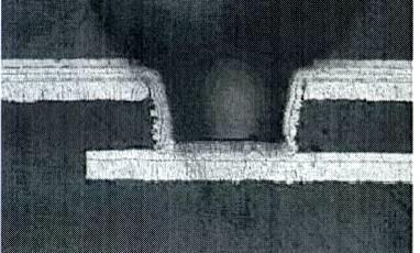
28 To Explore Further Hall and Heck give more in-depth treatments for topics relating to lossy transmission line systems: Skin effect, surface roughness, causality,and the relationship between frequency dependent L and R. Chapter 5 Dielectric losses, causality, the relationship between er and tand, the relationship between C and G. Chapter 6 Mathematical requirements for physical channels: Chapter 8 Modeling of transmission lines with losses Chapter 10 28

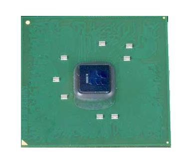
29 Background Connectors, packages, and vias are part of every major IA high speed interface. Understanding their performance and modeling is essential to successful interconnect design. Graphics Connector CPU Socket Chipset Package Memory Connectors 29
30 Agenda Vias Definition: what are they and why do we need them? Electrical models of via parasitics Connectors Definition: what are they and why do we need them? Electrical effects Packages Inductance SLEM-style approximation Power and ground pins Design considerations (tradeoffs, rules of thumb) Definition: what they are and why we need them Common types (e.g. flip-chip, bondwire) and history Creating package models Effect of a package on signal integrity Design considerations 30
31 Vias Vertical connections between layers made by drilling a small hole and filling it with conductive material. Vias connect metal layers on Silicon chips, within packages, and on printed circuit boards. vias capacitor chip chip pkg PCB 31
32 Via Functions Vias are typically used to Connect metal planes of the same potential (e.g., all ground planes conductively attached) Carry a signal from a trace on one layer to another Connect components (such as a capacitor) to a signal trace or a voltage plane. Provide probe points for testing production boards. 32

33 Via Structures Barrel: conductive cylinder filling the drilled hole Pad: connects the barrel to the component/plane/trace Antipad: clearance hole between via and no-connect metal layer Trace connected to pad on layer 1. Pad Barrel / Drill Via pad does not contact plane in this case; void is called the anti-pad 33
34 PCB Via Types Through Hole Via Blind Via Stepped Via Buried Via Stacked Via Filled or not 34
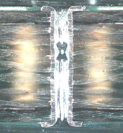
35 Via Cross-sections Laser generated via Stacked via Through hole via 35


36 Via Modeling As long as the delay through the via is <1/10 of the signal edge, we can model it as a lumped circuit. L barrel To red t-line C pad C pad D 1 Via pad diameter D 2 Via anti-pad diameter T PCB thickness C pad in pf h via length d barrel diameter L barrel in nh Via delay 36
 -40-60 -80-100 m2 freq=5.033ghz db(vin)=-94.045 m2 0 2 4 6 8 10 freq, GHz f R = 9.")
37 Resonance Due Via Stubs Via drill diameter: 28 mils Via pad diameter: 42 mils Via anti-pad diameter: 58 mils Board thickness: 62 mils C=0.4 pf, L=0.7 nh L barrel C pad C pad 0-20 db(vin) m2 freq=5.033ghz db(vin)= m freq, GHz f R = 9.5GHz delay ~ 17ps 37
38 Agenda Packages

39 Packages 39
40 Key Features (Cross-section view) Build-Up Core Build-Up Eutectic Solder Ball Grid Array (BGA) Chip Capacitor Integrated Circuit (Die) micro-via (uvia) Plated Through Hole (PTH) Pin Grid Array (BGA) Solder Resist (SR) Copper Layer Insulator (Dielectric) 40

41 Package Routing Small T-lines route from bond pad of package to the board attachment (e.g., pin or solder ball) High speed design requires controlled impedance A miniature PCB: layers, power/ground planes. Layers have well-defined impedance & routing rules that consider effects like crosstalk. 41
42 Package to PCB Attach Types Lead frame: metal frame connects wire bonds to PCB PGA: array of pins that stick out of the package BGA: array of solder balls that attach to board LGA: array of pads that attach to board LGA & PGA are socketable to provide Interchangeability (e.g., memory sticks, CPU upgrades) for OEM inventory control, the impact of tax and duty, and manufacturing flexibility. 42
43 Modeling of a Package with Socket Traces Via Transmission Line Sectioned Pi models Connector Lumped element sections Pwr/Gnd plane Ensure significant return path effects are modeled 43
44 Package Modeling Package Traces: coupling and x- sections Top-view of pkg D C Bondwire side-view and x-sections D B A A H A B Die C B B H A 44
45 Agenda Connectors
 Gold fingers locate near")

 DDR3 UDIMM connector DDR3 SODIMM")
46 Card Edge Connectors Connector is mounted on base board (PTH, PF, or SMT) Gold fingers locate near edge of module Module slide into the connector to establish connection to base board Example: PCIe; UDIMM, SODIMM, MXM PCIe connector (X4) Mini PCIe connector (X4) DDR3 UDIMM connector DDR3 SODIMM connector 46

47 Sockets 47

48 Connector Modeling Connector housing trace Plated Through Hole Connector contact in air & partially in housing Upper piece of contact & add-in card pad 48


49 Connector Models Series Loop Inductance a 2d a << d Parallel wires a radius of round wire l length d half distance between wires Approximate L between 2 connector loops Parallel loops g loop to loop spacing d half distance between wires l length 2d g 2d 49


50 Connector Models Capacitance Inductance a 2d a << d Parallel wires a radius of round wire l length d half distance between wires Approximate C between 2 connector loops Parallel loops g loop to loop spacing d half distance between wires l length 2d g 2d 50
51 Edge Finger Pad Model 28 mils = umeters 4.5 mils = micrometers 165 mils = 4191 um 28 mils = um Comparison of edge finger to connector pin shows that the edge finer capacitance is much larger. The pin capacitance and mutual capacitance between pins are negligible. 51
52 Connector Model Breakdown Connector housing trace 1.55 pf 3.13 nh 3.13 nh pf 1.0 pf Sectioned connector model need to ensure that there is enough sections for your frequency requirements. Is 1/TD of the section less than 1/10 a wavelength of the highest frequency of interest? 52
53 Multi-Gb/s Modeling: 3D Field Solver-Based PCIe DDR3 UDIMM SATA3 USB3 53
ECEN689: Special Topics in High-Speed Links Circuits and Systems Spring 2012
 ECEN689: Special Topics in High-Speed Links Circuits and Systems Spring 0 Lecture : Channel Components, Wires, & Transmission Lines Sam Palermo Analog & Mixed-Signal Center Texas A&M University Announcements
Transmission Line Basics II - Class 6
 Transmission Line Basics II - Class 6 Prerequisite Reading assignment: CH2 Acknowledgements: Intel Bus Boot Camp: Michael Leddige Agenda 2 The Transmission Line Concept Transmission line equivalent circuits
ECEN720: High-Speed Links Circuits and Systems Spring 2017
 ECEN70: High-Speed Links Circuits and Systems Spring 07 Lecture : Channel Components, Wires, & Transmission Lines Sam Palermo Analog & Mixed-Signal Center Texas A&M University Announcements Lab Lab begins
Non-Sinusoidal Waves on (Mostly Lossless)Transmission Lines
Transmission Lines") Non-Sinusoidal Waves on (Mostly Lossless)Transmission Lines Don Estreich Salazar 21C Adjunct Professor Engineering Science October 212 https://www.iol.unh.edu/services/testing/sas/tools.php 1 Outline of
Non-Sinusoidal Waves on (Mostly Lossless)Transmission Lines Don Estreich Salazar 21C Adjunct Professor Engineering Science October 212 https://www.iol.unh.edu/services/testing/sas/tools.php 1 Outline of
EECS 117 Lecture 3: Transmission Line Junctions / Time Harmonic Excitation
 EECS 117 Lecture 3: Transmission Line Junctions / Time Harmonic Excitation Prof. Niknejad University of California, Berkeley University of California, Berkeley EECS 117 Lecture 3 p. 1/23 Transmission Line
Topic 5: Transmission Lines
 Topic 5: Transmission Lines Profs. Javier Ramos & Eduardo Morgado Academic year.13-.14 Concepts in this Chapter Mathematical Propagation Model for a guided transmission line Primary Parameters Secondary
ECE 497 JS Lecture -03 Transmission Lines
 ECE 497 JS Lecture -03 Transmission Lines Spring 2004 Jose E. Schutt-Aine Electrical & Computer Engineering University of Illinois jose@emlab.uiuc.edu 1 MAXWELL S EQUATIONS B E = t Faraday s Law of Induction
Accounting for High Frequency Transmission Line Loss Effects in HFSS. Andrew Byers Tektronix
 Accounting for High Frequency Transmission Line Loss Effects in HFSS Andrew Byers Tektronix Transmission Line Refresher γ = α + j β = (R + jωl) * (G + jωc) Zo = Zr + j Zi = (R + jωl) / (G + jωc) Transmission
TC 412 Microwave Communications. Lecture 6 Transmission lines problems and microstrip lines
 TC 412 Microwave Communications Lecture 6 Transmission lines problems and microstrip lines RS 1 Review Input impedance for finite length line Quarter wavelength line Half wavelength line Smith chart A
ECE 451 Transmission Lines & Packaging
 Transmission Lines & Packaging Jose E. Schutt-Aine Electrical & Computer Engineering University of Illinois jose@emlab.uiuc.edu 1 Radio Spectrum Bands The use of letters to designate bands has long ago
Power Distribution Network Design for High-Speed Printed Circuit Boards
 Power Distribution Network Design for High-Speed Printed Circuit Boards Jun Fan NCR Corporation 1 Outline Overview of PDN design in multi-layer PCBs Interconnect Inductance Individual Capacitor Values
Kimmo Silvonen, Transmission lines, ver
 Kimmo Silvonen, Transmission lines, ver. 13.10.2008 1 1 Basic Theory The increasing operating and clock frequencies require transmission line theory to be considered more and more often! 1.1 Some practical
ECE414/514 Electronics Packaging Spring 2012 Lecture 6 Electrical D: Transmission lines (Crosstalk) Lecture topics
 Lecture topics") ECE414/514 Electronics Packaging Spring 2012 Lecture 6 Electrical D: Transmission lines (Crosstalk) James E. Morris Dept of Electrical & Computer Engineering Portland State University 1 Lecture topics
ECE414/514 Electronics Packaging Spring 2012 Lecture 6 Electrical D: Transmission lines (Crosstalk) James E. Morris Dept of Electrical & Computer Engineering Portland State University 1 Lecture topics
1.3 Sinusoidal Steady State
 1.3 Sinusoidal Steady State Electromagnetics applications can be divided into two broad classes: Time-domain: Excitation is not sinusoidal (pulsed, broadband, etc.) Ultrawideband communications Pulsed
ECEN689: Special Topics in High-Speed Links Circuits and Systems Spring 2012
 ECEN689: pecial Topics in High-peed Links Circuits and ystems pring 01 Lecture 3: Time-Domain Reflectometry & -Parameter Channel Models am Palermo Analog & Mixed-ignal Center Texas A&M University Announcements
GMII Electrical Specification Options. cisco Systems, Inc.
 DC Specifications GMII Electrical Specification Options Mandatory - Communication between the transmitter and receiver can not occur at any bit rate without DC specifications. AC Specifications OPTION
ESE 570: Digital Integrated Circuits and VLSI Fundamentals
 ESE 570: Digital Integrated Circuits and VLSI Fundamentals Lec 24: April 19, 2018 Crosstalk and Wiring, Transmission Lines Lecture Outline! Crosstalk! Repeaters in Wiring! Transmission Lines " Where transmission
! Crosstalk. ! Repeaters in Wiring. ! Transmission Lines. " Where transmission lines arise? " Lossless Transmission Line.
 ESE 570: Digital Integrated Circuits and VLSI Fundamentals Lec 24: April 19, 2018 Crosstalk and Wiring, Transmission Lines Lecture Outline! Crosstalk! Repeaters in Wiring! Transmission Lines " Where transmission
Transmission Line Basics
 Transmission Line Basics Prof. Tzong-Lin Wu NTUEE 1 Outlines Transmission Lines in Planar structure. Key Parameters for Transmission Lines. Transmission Line Equations. Analysis Approach for Z and T d
Announcements. EE141- Fall 2002 Lecture 25. Interconnect Effects I/O, Power Distribution
 - Fall 2002 Lecture 25 Interconnect Effects I/O, Power Distribution Announcements Homework 9 due next Tuesday Hardware lab this week Project phase 2 due in two weeks 1 Today s Lecture Impact of interconnects»
ECE 451 Advanced Microwave Measurements. TL Characterization
 ECE 451 Advanced Microwave Measurements TL Characterization Jose E. Schutt-Aine Electrical & Computer Engineering University of Illinois jesa@illinois.edu ECE 451 Jose Schutt-Aine 1 Maxwell s Equations
Understanding EMC Basics
 1of 7 series Webinar #1 of 3, February 27, 2013 EM field theory, and 3 types of EM analysis Webinar Sponsored by: EurIng CEng, FIET, Senior MIEEE, ACGI AR provides EMC solutions with our high power RF/Microwave
High Speed Communication Circuits and Systems Lecture 4 Generalized Reflection Coefficient, Smith Chart, Integrated Passive Components
 High Speed Communication Circuits and Systems Lecture 4 Generalized Reflection Coefficient, Smith Chart, Integrated Passive Components Michael H. Perrott February 11, 2004 Copyright 2004 by Michael H.
AN B. Basic PCB traces transmission line effects causing signal integrity degradation simulation using Altium DXP version 6.
 AN200805-01B Basic PCB traces transmission line effects causing signal integrity degradation simulation using Altium DXP version 6.9 By Denis Lachapelle eng. and Anne Marie Coutu. May 2008 The objective
Improving Power Delivery Networks (PDNs) Using Polyimide-based Thin Laminates
 Using Polyimide-based Thin Laminates") Improving Power Delivery Networks (PDNs) Using Polyimide-based Thin Laminates 2017. 7. 19. 1 Contents 1. Embedded passives technology 2. Thin laminates: material choices and applications 3. Buried capacitance
Improving Power Delivery Networks (PDNs) Using Polyimide-based Thin Laminates 2017. 7. 19. 1 Contents 1. Embedded passives technology 2. Thin laminates: material choices and applications 3. Buried capacitance
SRAM System Design Guidelines
 Introduction This application note examines some of the important system design considerations an engineer should keep in mind when designing with Cypress SRAMs. It is important to note that while they
AMD Socket 940 Qualification Plan
 AMD Socket 940 Qualification Plan Publication # 30353 Revision: 3.04 Issue Date: September 2003 2003 Advanced Micro Devices, Inc. All rights reserved. The contents of this document are provided in connection
Graser User Conference Only
 PCB Power Delivery Design from DC to Mid-Frequency Foxconn Abby Chou Company Introduction February 1974 Tucheng District 1.23 million Server Storage Mobile Phone Pad TV Voltage Drop and Thermal Co-Simulation
Characterization of a Printed Circuit Board Via
 Characterization of a Printed Circuit Board Via Brock J. LaMeres Thesis Defense May 25, 2000 Department of Electrical and Computer Engineering University of Colorado Colorado Springs, CO Objective To Develop
Keysight Technologies Heidi Barnes
 Keysight Technologies 2018.03.29 Heidi Barnes 1 S I G N A L I N T E G R I T Y A N D P O W E R I N T E G R I T Y Hewlett-Packard Agilent Technologies Keysight Technologies Bill and Dave s Company and the
Complex Numbers, Phasors and Circuits
 Complex Numbers, Phasors and Circuits Transmission Lines Complex numbers are defined by points or vectors in the complex plane, and can be represented in Cartesian coordinates or in polar (exponential)
TRANSMISSION LINES AND MATCHING
 TRANSMISSION LINES AND MATCHING for High-Frequency Circuit Design Elective by Michael Tse September 2003 Contents Basic models The Telegrapher s equations and solutions Transmission line equations The
Electromagnetic Modeling and Signal Integrity Simulation of Power/Ground Networks in High Speed Digital Packages and Printed Circuit Boards
 Electromagnetic Modeling and Signal Integrity Simulation of Power/Ground Networks in High Speed Digital Packages and Printed Circuit Boards Frank Y. Yuan Viewlogic Systems Group, Inc. 385 Del Norte Road
ECE 497 JS Lecture - 18 Noise in Digital Circuits
 ECE 497 JS Lecture - 18 Noise in Digital Circuits Spring 2004 Jose E. Schutt-Aine Electrical & Computer Engineering University of Illinois jose@emlab.uiuc.edu 1 Announcements Thursday April 15 th Speaker:
Analytic Solutions for Periodically Loaded Transmission Line Modeling
 Analytic Solutions for Periodically Loaded Transmission Line Modeling Paul G. Huray, huray@sc.edu Priya Pathmanathan, Intel priyap@qti.qualcomm.com Steve Pytel, Intel steve.pytel@ansys.com April 4, 2014
Lecture 21: Packaging, Power, & Clock
 Lecture 21: Packaging, Power, & Clock Outline Packaging Power Distribution Clock Distribution 2 Packages Package functions Electrical connection of signals and power from chip to board Little delay or
Rg2 Lg2 Rg6 Lg6 Rg7 Lg7. PCB Trace & Plane. Figure 1 Bypass Decoupling Loop
 TECHNICAL NOTE This article was originally published in 1996. INTRODUCTION In order to guarantee better performance from highspeed digital integrated circuits (ICs), manufacturers are tightening power
Transmission Lines in the Frequency Domain
 Berkeley Transmission Lines in the Frequency Domain Prof. Ali M. Niknejad U.C. Berkeley Copyright c 2016 by Ali M. Niknejad August 30, 2017 1 / 38 Why Sinusoidal Steady-State? 2 / 38 Time Harmonic Steady-State
Considerations for Capacitor Selection in FPGA Designs
 Considerations for Capacitor Selection in FPGA Designs Steve Weir Steve Weir Design Engineering & Teraspeed Consulting Group 2036 Clydesdale Way Petaluma, CA 94954 Voice (775) 762-9031 FAX (707) 778-9386
ECE 546 Lecture 04 Resistance, Capacitance, Inductance
 ECE 546 Lecture 04 Resistance, Capacitance, Inductance Spring 2018 Jose E. Schutt-Aine Electrical & Computer Engineering University of Illinois jschutt@emlab.uiuc.edu ECE 546 Jose Schutt Aine 1 What is
The Wire. Digital Integrated Circuits A Design Perspective. Jan M. Rabaey Anantha Chandrakasan Borivoje Nikolic. July 30, 2002
 Digital Integrated Circuits A Design Perspective Jan M. Rabaey Anantha Chandrakasan Borivoje Nikolic The Wire July 30, 2002 1 The Wire transmitters receivers schematics physical 2 Interconnect Impact on
Broadband transmission line models for analysis of serial data channel interconnects
 PCB Design Conference East, Durham NC, October 23, 2007 Broadband transmission line models for analysis of serial data channel interconnects Y. O. Shlepnev, Simberian, Inc. shlepnev@simberian.com Simberian:
November MVP R&S FSW Analyzer. Vol. 54 No. 11. Founded in mwjournal.com
 Vol. 54 No. 11 November 211 MVP R&S FSW Analyzer Founded in 1958 mwjournal.com Improved Thermal Management of Microwave PCBs Using Advanced Circuit Materials Thermal management in microwave printed-circuit
and Ee = E ; 0 they are separated by a dielectric material having u = io-s S/m, µ, = µ, 0
 602 CHAPTER 11 TRANSMISSION LINES 11.10 Two identical pulses each of magnitude 12 V and width 2 µs are incident at t = 0 on a lossless transmission line of length 400 m terminated with a load. If the two
Modeling copper cables and PCBs
 Chapter 2 Modeling copper cables and PCBs 2.1. Introduction A proper channel model is a good basis for a correct understanding of any transmission system. The goal of this chapter is to identify an accurate
Modeling of Signal and Power Integrity in System on Package Applications
 Modeling of Signal and Power Integrity in System on Package Applications Madhavan Swaminathan and A. Ege Engin Packaging Research Center, School of Electrical and Computer Engineering, Georgia Institute
Equivalent Circuit Model Extraction for Interconnects in 3D ICs
 Equivalent Circuit Model Extraction for Interconnects in 3D ICs A. Ege Engin Assistant Professor, Department of ECE, San Diego State University Email: aengin@mail.sdsu.edu ASP-DAC, Jan. 23, 213 Outline
Transient Response of Transmission Lines and TDR/TDT
 Transient Response of Transmission Lines and TDR/TDT Tzong-Lin Wu, Ph.D. EMC Lab. Department of Electrical Engineering National Sun Yat-sen University Outlines Why do we learn the transient response of
Modification of Signal Propagation Velocity Through Printed Circuit Boards Using High Dielectric Constant Materials
 Modification of Signal Propagation Velocity Through Printed Circuit Boards Using High Dielectric Constant Materials RICHARD JIANG, BROWN UNIVERSITY DOUGLAS JACKSON, UNIVERSITY OF LOUISVILLE JOHN NABER,
Next-Generation Packaging Technology for Space FPGAs
 Power Matters. Next-Generation Packaging Technology for Space FPGAs Microsemi Space Forum Russia November 2013 Raymond Kuang Director of Packaging Engineering, SoC Products Group Agenda CCGA (ceramic column
Interconnect s Role in Deep Submicron. Second class to first class
 Interconnect s Role in Deep Submicron Dennis Sylvester EE 219 November 3, 1998 Second class to first class Interconnect effects are no longer secondary # of wires # of devices More metal levels RC delay
ECE 598 JS Lecture 06 Multiconductors
 ECE 598 JS Lecture 06 Multiconductors Spring 2012 Jose E. Schutt-Aine Electrical & Computer Engineering University of Illinois jesa@illinois.edu 1 TELGRAPHER S EQUATION FOR N COUPLED TRANSMISSION LINES
SCSI Connector and Cable Modeling from TDR Measurements
 SCSI Connector and Cable Modeling from TDR Measurements Dima Smolyansky TDA Systems, Inc. http://www.tdasystems.com Presented at SCSI Signal Modeling Study Group Rochester, MN, December 1, 1999 Outline
Causal Modeling and Extraction of Dielectric Constant and Loss Tangent for Thin Dielectrics
 Causal Modeling and Extraction of Dielectric Constant and Loss Tangent for Thin Dielectrics A. Ege Engin 1, Abdemanaf Tambawala 1, Madhavan Swaminathan 1, Swapan Bhattacharya 1, Pranabes Pramanik 2, Kazuhiro
PRODUCT SPECIFICATION
 1 of 10 H 1.0 GENERAL THIS SPECIFICATION COVERS.039 INCHES VERTICAL DDR II SOCKETS WITH BLANKED / FORMED CONTACT DESIGNED FOR PRINTED WIRING BOARD TO DUAL IN-LINE MEMORY MODULE INTERCONNECTION. IN ALL
Analysis of TSV-to-TSV Coupling with High-Impedance Termination in 3D ICs
 Analysis of -to- Coupling with -Impedance Termination in 3D ICs Taigon Song, Chang Liu, Dae Hyun Kim, and Sung Kyu Lim School of Electrical and Computer Engineering, Georgia Institute of Technology, U.S.A.
EMC Considerations for DC Power Design
 EMC Considerations for DC Power Design Tzong-Lin Wu, Ph.D. Department of Electrical Engineering National Sun Yat-sen University Power Bus Noise below 5MHz 1 Power Bus Noise below 5MHz (Solution) Add Bulk
How to measure complex impedance at high frequencies where phase measurement is unreliable.
 Objectives In this course you will learn the following Various applications of transmission lines. How to measure complex impedance at high frequencies where phase measurement is unreliable. How and why
Interconnect (2) Buffering Techniques.Transmission Lines. Lecture Fall 2003
 Buffering Techniques.Transmission Lines. Lecture Fall 2003") Interconnect (2) Buffering Techniques.Transmission Lines Lecture 12 18-322 Fall 2003 A few announcements Partners Lab Due Times Midterm 1 is nearly here Date: 10/14/02, time: 3:00-4:20PM, place: in class
Interconnect (2) Buffering Techniques.Transmission Lines Lecture 12 18-322 Fall 2003 A few announcements Partners Lab Due Times Midterm 1 is nearly here Date: 10/14/02, time: 3:00-4:20PM, place: in class
Broadband material model identification with GMS-parameters
 Broadband material model identification with GMS-parameters Yuriy Olegovich Shlepnev Simberian Inc. shlepnev@simberian.com 2015 EPEPS Conference, October 27, 2015 2015 Simberian Inc. Outline Introduction
Differential Impedance finally made simple
 Slide - Differential Impedance finally made simple Eric Bogatin President Bogatin Enterprises 93-393-305 eric@bogent.com Slide -2 Overview What s impedance Differential Impedance: a simple perspective
Introduction to RF Design. RF Electronics Spring, 2016 Robert R. Krchnavek Rowan University
 Introduction to RF Design RF Electronics Spring, 2016 Robert R. Krchnavek Rowan University Objectives Understand why RF design is different from lowfrequency design. Develop RF models of passive components.
AN ABSTRACT OF THE THESIS OF
 AN ABSTRACT OF THE THESIS OF Chris Blevins for the degree of Master of Science in Electrical and Computer Engineering presented on April 16, 2010. Title: Model Development Via Delay Extraction for the
The Wire EE141. Microelettronica
 The Wire 1 Interconnect Impact on Chip 2 Example: a Bus Network transmitters receivers schematics physical 3 Wire Models All-inclusive model Capacitance-only 4 Impact of Interconnect Parasitics Interconnect
Characteristics of Passive IC Devices
 008/Oct 8 esistors Characteristics of Passive IC Devices Poly esistance Diffusion esistance Well esistance Parasitic esistance Capacitors Poly Capacitors MOS Capacitors MIM Capacitors Parasitic Capacitors
IBIS EBD Modeling, Usage and Enhancement An Example of Memory Channel Multi-board Simulation
 IBIS EBD Modeling, Usage and Enhancement An Example of Memory Channel Multi-board Simulation Tao Xu Asian IBIS Summit taoxu@sigrity.com Shanghai China November 11, 2008 Agenda Memory channel simulation
Five Myths about the PDN
 Slide -1 A copy of the slides is available on www.bethesignal.com: search VL-180 or PPT-180 Five Myths about the PDN Eric Bogatin, eric@bethesignal.com Signal Integrity Evangelist Bogatin Enterprises www.bethesignal.com
INTRODUCTION TO TRANSMISSION LINES DR. FARID FARAHMAND FALL 2012
 INTRODUCTION TO TRANSMISSION LINES DR. FARID FARAHMAND FALL 2012 http://www.empowermentresources.com/stop_cointelpro/electromagnetic_warfare.htm RF Design In RF circuits RF energy has to be transported
ESE 570: Digital Integrated Circuits and VLSI Fundamentals
 ESE 570: Digital Integrated Circuits and VLSI Fundamentals Lec 23: April 17, 2018 I/O Circuits, Inductive Noise, CLK Generation Lecture Outline! Packaging! Variation and Testing! I/O Circuits! Inductive
ECE 497 JS Lecture -07 Planar Transmission Lines
 ECE 497 JS Lecture -07 Planar Transmission Lines Spring 2004 Jose E. Schutt-Aine Electrical & Computer Engineering University of Illinois jose@emlab.uiuc.edu 1 Microstrip ε Z o w/h < 3.3 2 119.9 h h =
ARIES: Using Annular-Ring Embedded Resistors to Set Capacitor ESR in Power Distribution Networks
 St.,Cyr-Novak-Biunno-Howard: Using Embedded Resistors to Set Capacitor ESR in Power Distribution Networks. ARIES: Using Annular-Ring Embedded Resistors to Set Capacitor ESR in Power Distribution Networks
POWERING DIGITAL BOARDS
 POWERING DIGITAL BOARDS DISTRIBUTION AND PERFORMANCE Istvan Novak, Signal Integrity Staff Engineer SUN Microsystems, Inc. Meeting of the Greater Boston Chapter IPC Designer's Council February 9, 1999 1
X2Y Capacitors for FPGA Decoupling
 Summary Introduction FPGA Decoupling X2Y capacitors provide advantages to FPGA decoupling applications unmatched by any other devices in the market. High performance, low-voltage FPGAs demand low impedance
PDN Planning and Capacitor Selection, Part 2
 by Barry Olney column BEYOND DESIGN PDN Planning and Capacitor Selection, Part 2 In last month s column, PDN Planning and Capacitor Selection Part 1, we looked closely at how to choose the right capacitor
ESE 570: Digital Integrated Circuits and VLSI Fundamentals
 ESE 570: Digital Integrated Circuits and VLSI Fundamentals Lec 23: April 13, 2017 Variation; I/O Circuits, Inductive Noise Lecture Outline! Design Quality " Variation! Packaging! Variation and Testing!
EECS 151/251A Spring 2018 Digital Design and Integrated Circuits. Instructors: Nick Weaver & John Wawrzynek. Lecture 12 EE141
 EECS 151/251A Spring 2018 Digital Design and Integrated Circuits Instructors: Nick Weaver & John Wawrzynek Lecture 12 1 Wire Models All-inclusive model Capacitance-only 2 Capacitance Capacitance: The Parallel
Education, Xidian University, Xi an, Shaanxi , China
 Progress In Electromagnetics Research, Vol. 142, 423 435, 2013 VERTICAL CASCADED PLANAR EBG STRUCTURE FOR SSN SUPPRESSION Ling-Feng Shi 1, 2, * and Hong-Feng Jiang 1, 2 1 Key Lab of High-Speed Circuit
ECE 107: Electromagnetism
 ECE 107: Electromagnetism Set 2: Transmission lines Instructor: Prof. Vitaliy Lomakin Department of Electrical and Computer Engineering University of California, San Diego, CA 92093 1 Outline Transmission
Experiment 06 - Extraction of Transmission Line Parameters
 ECE 451 Automated Microwave Measurements Laboratory Experiment 06 - Extraction of Transmission Line Parameters 1 Introduction With the increase in both speed and complexity of mordern circuits, modeling
ANTENNAS and MICROWAVES ENGINEERING (650427)
") Philadelphia University Faculty of Engineering Communication and Electronics Engineering ANTENNAS and MICROWAVES ENGINEERING (65427) Part 2 Dr. Omar R Daoud 1 General Considerations It is a two-port network
Philadelphia University Faculty of Engineering Communication and Electronics Engineering ANTENNAS and MICROWAVES ENGINEERING (65427) Part 2 Dr. Omar R Daoud 1 General Considerations It is a two-port network
Digital Integrated Circuits. The Wire * Fuyuzhuo. *Thanks for Dr.Guoyong.SHI for his slides contributed for the talk. Digital IC.
 Digital Integrated Circuits The Wire * Fuyuzhuo *Thanks for Dr.Guoyong.SHI for his slides contributed for the talk Introduction The Wire transmitters receivers schematics physical 2 Interconnect Impact
Distributed SPICE Circuit Model for Ceramic Capacitors
 Published in Conference Record, Electrical Components Technology Conference (ECTC), Lake Buena Vista, Florida, pp. 53-58, May 9, 00. Distributed SPICE Circuit Model for Ceramic Capacitors Larry D Smith,
0805 CG 102 J 500 N T
 NPO/COG for General-use is class I high frequency capacitor, its capacitance is very stable, almost will not change along with the temperature, voltage and time. Specially be suitable for high frequency
TASK A. TRANSMISSION LINE AND DISCONTINUITIES
 TASK A. TRANSMISSION LINE AND DISCONTINUITIES Task A. Transmission Line and Discontinuities... 1 A.I. TEM Transmission Line... A.I.1. Circuit Representation of a Uniform Transmission Line... A.I.. Time
Lecture 2 - Transmission Line Theory
 Lecture 2 - Transmission Line Theory Microwave Active Circuit Analysis and Design Clive Poole and Izzat Darwazeh Academic Press Inc. Poole-Darwazeh 2015 Lecture 2 - Transmission Line Theory Slide1 of 54
Transmission Line Theory
 S. R. Zinka zinka@vit.ac.in School of Electronics Engineering Vellore Institute of Technology April 26, 2013 Outline 1 Free Space as a TX Line 2 TX Line Connected to a Load 3 Some Special Cases 4 Smith
LOSSY TRANSMISSION LINE MODELING AND SIMULATION USING SPECIAL FUNCTIONS
 LOSSY TRANSMISSION LINE MODELING AND SIMULATION USING SPECIAL FUNCTIONS by Bing Zhong A Dissertation Submitted to the Faculty of the DEPARTMENT OF ELECTRICAL AND COMPUTER ENGINEERING In Partial Fulfillment
Time Domain Modeling of Lossy Interconnects
 IEEE TRANSACTIONS ON ADVANCED PACKAGING, VOL. 24, NO. 2, MAY 2001 191 Time Domain Modeling of Lossy Interconnects Christer Svensson, Member, IEEE, and Gregory E. Dermer Abstract A new model for dielectric
Waves on Lines. Contents. ! Transmission Lines! The Smith Chart! Vector Network Analyser (VNA) ! Measurements
 ! Measurements") Waves on Lines If the wavelength to be considered is significantly greater compared to the size of the circuit the voltage will be independent of the location. amplitude d! distance but this is not true
Waves on Lines If the wavelength to be considered is significantly greater compared to the size of the circuit the voltage will be independent of the location. amplitude d! distance but this is not true
Lecture 040 Integrated Circuit Technology - II (5/11/03) Page ECE Frequency Synthesizers P.E. Allen
 Page ECE Frequency Synthesizers P.E. Allen") Lecture 040 Integrated Circuit Technology - II (5/11/03) Page 040-1 LECTURE 040 INTEGRATED CIRCUIT TECHNOLOGY - II (Reference [7,8]) Objective The objective of this presentation is: 1.) Illustrate and
Lecture 040 Integrated Circuit Technology - II (5/11/03) Page 040-1 LECTURE 040 INTEGRATED CIRCUIT TECHNOLOGY - II (Reference [7,8]) Objective The objective of this presentation is: 1.) Illustrate and
Lecture 23. Dealing with Interconnect. Impact of Interconnect Parasitics
 Lecture 23 Dealing with Interconnect Impact of Interconnect Parasitics Reduce Reliability Affect Performance Classes of Parasitics Capacitive Resistive Inductive 1 INTERCONNECT Dealing with Capacitance
PHY3128 / PHYM203 (Electronics / Instrumentation) Transmission Lines
 Transmission Lines") Transmission Lines Introduction A transmission line guides energy from one place to another. Optical fibres, waveguides, telephone lines and power cables are all electromagnetic transmission lines. are
Transmission Lines Introduction A transmission line guides energy from one place to another. Optical fibres, waveguides, telephone lines and power cables are all electromagnetic transmission lines. are
UNIT I ELECTROSTATIC FIELDS
 UNIT I ELECTROSTATIC FIELDS 1) Define electric potential and potential difference. 2) Name few applications of gauss law in electrostatics. 3) State point form of Ohm s Law. 4) State Divergence Theorem.
A Method to Extract Dielectric Parameters from Transmission Lines with Conductor Surface Roughness at Microwave Frequencies
 Progress In Electromagnetics Research M, Vol. 48, 1 8, 2016 A Method to Extract Dielectric Parameters from Transmission Lines with Conductor Surface Roughness at Microwave Frequencies Binke Huang * and
112 Gbps In and Out of Package Challenges Design insights from electromagnetic analysis. Yuriy Shlepnev, Simberian Inc.
 112 Gbps In and Out of Package Challenges Design insights from electromagnetic analysis Yuriy Shlepnev, Simberian Inc. shlepnev@simberian.com Package and PCB scales in symbol time for 112 Gbps PAM4 Package:
Analytic Solutions for Periodically Loaded Transmission Line Modeling
 DesignCon 2013 Analytic Solutions for Periodically Loaded Transmission Line Modeling Priya Pathmanathan, Intel Corporation priya.pathmanathan@intel.com Paul G. Huray, University of South Carolina huray@sc.edu
ARCHIVE INFORMATION ARCHIVE INFORMATION SEMICONDUCTOR AN1061 REFLECTING ON TRANSMISSION LINE EFFECTS MOTOROLA APPLICATION NOTE
 MOTOROLA SEMICONDUCTOR APPLICATION NOTE Order this document by AN1061/D AN1061 REFLECTING ON TRANSMISSION LINE EFFECTS This application note describes introductory transmission line characterization, analysis,
TECHNICAL INFORMATION
 TECHNICAL INFORMATION LICA (LOW INDUCTANCE CAPACITOR ARRAY) FLIP-CHIP APPLICATION NOTES by Jeff Cantlebary AVX Corporation LICA (LOW INDUCTANCE CAPACITOR ARRAY) FLIP-CHIP APPLICATION NOTES Introduction
EFFICIENT STRATEGIES TO OPTIMIZE A POWER DISTRIBUTION NETWORK
 EFFICIENT STRATEGIES TO OPTIMIZE A POWER DISTRIBUTION NETWORK Raul FIZEŞAN, Dan PITICĂ Applied Electronics Department of UTCN 26-28 Baritiu Street, Cluj-Napoca, raul.fizesan@ael.utcluj.ro Abstract: One
Modeling frequency-dependent conductor losses and dispersion in serial data channel interconnects
 Modeling frequency-dependent conductor losses and dispersion in serial data channel interconnects Yuriy Shlepnev Simberian Inc., www.simberian.com Abstract: Models of transmission lines and transitions