EMC Considerations for DC Power Design
|
|
|
- Charles Williams
- 5 years ago
- Views:
Transcription
1 EMC Considerations for DC Power Design Tzong-Lin Wu, Ph.D. Department of Electrical Engineering National Sun Yat-sen University Power Bus Noise below 5MHz 1
2 Power Bus Noise below 5MHz (Solution) Add Bulk capacitance Power Bus Noise between 5MHz to 50MHz 2
3 Power Bus Noise between 5MHz to 50MHz (Solution) Power Bus Noise between 50MHz to 500MHz 3
4 Power Bus Noise between 50MHz to 500MHz (Solution) RF Path in power bus (I) 5V bypass capacitor Case 1 Vcc pin 3.3V bypass Signal pin capacitor A B C Signal current Return current S1 G 5V S2 S3 S4 S5 3.3V G S6 * Bypass capacitor provide return currents to flow from plane to plane 4
5 RF Path in power bus (II) Case 2 Vcc pin Signal current Signal pin 5V bypass Return current capacitor A Via B S1(H) Pair A GND C S2(V) Pair A S3(H) Pair C GND 5V and 3.3V split S4(V) Pair C S5(H) Pair B GND S6(V) Pair B * Bypass capacitor provide return currents to flow from plane to plane A simple power bus model 100 nh A=10 in p N= Impedance (Ω) Series resonance Parallel resonance of L tot and C bulk Frequency (Hz) Wiring inductance 10μF 0.1Ω 32*0.016μF 0.1Ω Power and ground plane capacitance 5


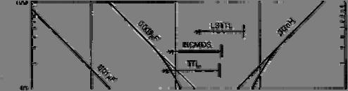
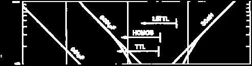
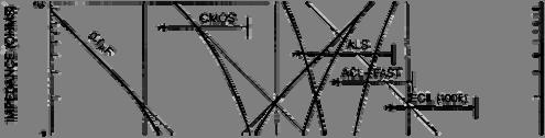
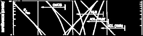
6 Power Bus Impedance Power Bus Impedance (an example) If the Moore s Law and CMOS scaling is to continue, the power bus Design will be increasingly difficult design problems. 6


7 Voltage Regulator Module (VRM) The VRM converts one DC voltage to another, for example 5V to 1.8V. It has a reference voltage and a feedback loop. The bandwidth of the regulation loop is usually between 1kHz to several hundred khz. At frequencies above the loop bandwidth, the VRM becomes high impedance. Voltage Regulator Module (VRM) : working mechanism Inductor 1. S1 close, S2 open : load is demanding current, L1 is storing energy. 2. If L1 supply more current than the load demanding, S1 open, S2 close. 3. Current continues to flow to the load until S2 opens, S1 closes again. Capacitor C1 smoothes out the voltage. Amplifier A 1. When the load voltage is too low, it causes the switches and inductor to ramp up the current. 2. When the load voltage is too high, it causes the switches and inductor to ramp down the current. 7

 Or the inductance of the pins connecting the VRM to the CPU module (4nH) 3.")
8 Voltage Regulator Module (VRM) : linear model 1. The buck regulator is nonlinear because switches open and closed as a function of time. 2. A linear model of VRM is necessary in the design phase of the Power Bus. 3. The linear model below is accurate enough to estimate the amount of the bulk capacitance. 1. R0 is the value of the resistor between VRM sense point and the actual load. 2. L_out is the output inductance It may be the cables that connect the VRM to the system board (200nH) Or the inductance of the pins connecting the VRM to the CPU module (4nH) 3. R_flat is the ESR of the capacitor associated with the VRM. 4. What is the L_slew and its value? Voltage Regulator Module (VRM) : linear model 1. L_slew is the only element in the linear model that is not traceable back to an element in the nonlinear VRM model. 2. The value of L_slew is chosen so that current will be ramped up in the linear model in about the same time that it is ramped up in a real VRM. For example Typical parameters for a VRM attached on a processor module 8


9 VRM : behavior example Impedance V.S. Frequency 10m ohm 1m ohm Target impedance 10kHz VRM : behavior example VRM voltage v.s. time transient Over spec. Why? 9


10 Bulk Capacitance Bulk capacitors are necessary to maintain the power bus impedance at frequencies above those maintained by the VRM and below the frequencies where ceramic capacitors are effective. The capacitance value can be roughly estimated by Δt C = I Δ V Ex: For 20A current transient, the VRM responds in 15us, and the PDS should remain in 5% of 1.8V. Does the capacitance value enough or over? Bulk Capacitance: frequency response A: This estimation maybe overestimate the required bulk capacitance by a factor 2 because The VRM is ramping up current and the average current may be half of the final value during the VRM response time. 1 ohm 2700uF 0.1 ohm 33uF 330uF Bulk capacitance can be modeled by the series of RLC 0.01 ohm 10000uF Y5V 100uF X5R 22uF 1kHz 1MHz 10MHz 10


11 Bulk Capacitance: behavior Output impedance v.s. frequency when a VRM is placed in parallel with 5 x 2700uF electrolytic bulk capacitance The impedance is under spec up to almost 1MHz Bulk Capacitance: behavior 20A current transients at 100kHz with 200ns rise/fall time Over spec (5%), why? 11


12 High Frequency Ceramic Capacitance: Type Dielectric type ESR Reliability Value NPO X7R lowest dependent best good Up to a few nf Several nf to several uf Package size: X5R dependent fair Several nf to 100 uf Y5V dependent Poor High capacitance High Frequency Ceramic Capacitance: Model real model Ideal model 12
13 Ceramic Capacitance: Model behavior cap2 cap3 cap1 cap2 depth The depth is decided by what? The resonance frequency is decided by what? Ceramic Capacitance: Model behavior 13

14 ESR of Ceramic Capacitance ESR can be measured by the HP4291A (Impedance Analyzer) by a SMA testing fixture A better technique employing the low impedance head connected to the IA. ESL of Ceramic Capacitance Who contributes the ESL of the decoupling capacitor?? 14

15 ESL of Ceramic Capacitance There are THREE components of the ESL. 1. Pad layout 2. Capacitor height 3. Power plane spreading inductance ESL of Ceramic Capacitance : Pad inductance The pad layout consists of 1. Via placement with respect to the pad 2. The length and width of the traces connected to the pad 3. The way the via is connected to the power/ground planes Which parts dominate the ESL of the pad layout?? 15


16 ESL of Ceramic Capacitance : Pad inductance ϕ L I ϕ = B ds The location of the power/ground in the PCB stackup controls the height of the via which is the major contributor of the pad inductance. Magnetic field concentrate between two vias and negligible outside. Reducing the loop area will decrease the ESL ESL of Ceramic Capacitance : Pad inductance 16


17 ESL of Ceramic Capacitance : Capacitance height For thicker capacitor, the current has to flow up and down and effectively increase the length of the current loop ESL of Ceramic Capacitance : PWR/GND spreading inductance The last factor contributing to the ESL is the Spreading inductance between the PWR/GND. What is the meaning of the spreading inductance? 17
18 ESL of Ceramic Capacitance : PWR/GND spreading inductance What is the meaning of the spreading inductance? GND PWR spreading inductance CAP PWR GND VIA VIA ESL of Ceramic Capacitance : PWR/GND spreading inductance corner edge center Which one has larger spreading inductance? Why? 18
19 ESL of Ceramic Capacitance : PWR/GND spreading inductance Corner 1. Edge 2. Center 3. ESL of Ceramic Capacitance : PWR/GND spreading inductance Spreading inductance for different via locations for various plane separations 19

20 ESL of Ceramic Capacitance : Comparison 1. Pad layout 2. Capacitor height 3. Power plane spreading inductance Which one is the main contributor of the ESL?? CAP PWR GND VIA VIA ESL of Ceramic Capacitance : Comparison nf Pad inductance is the dominant factor for minimizing the power plane separations. 20


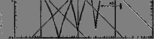
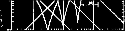
21 Shunting of Ceramic Capacitance :Identical capacitors 1ohm 0.1ohm Identical capacitors in parallel. The impedance is reduced by a factor of 2 every time the quantity is doubled. 0.01ohm 100MHz 1GHz Shunting of Ceramic Capacitance: different values A peak : Anti-resonance Why? 21


22 Shunting of Ceramic Capacitance: different values LC in parallel resonance C L LC series resonance LC series resonance How to reduce the peak of the anti-resonance to meet the target impedance?? Shunting of Ceramic Capacitance: different values Minimizing the ESL is the most effective way to reduce the height of the peak. 22


23 Shunting of Ceramic Capacitance: different values The anti-resonance also becomes high if large gaps exist in capacitive value. Three capacitors are used but with the total values being equal to the previous case. Impedance of Ceramic Capacitance What capacitor behavior do you see?? 23


24 Impedance of Ceramic Capacitance 1. The resonance frequency goes up as the capacitance value decreases. Why? (ESL decreases) 2. The minimum impedance did not go down as the capacitance value decreases. Why? (ESR is lower for higher capacitive values) So, Parallel the capacitor is necessary for meeting the target impedance at high frequencies. Impedance of a complete power bus Impedance v.s. frequency of PDS with VRM, 7 bulk capacitors, 115 ceramic capacitors. The PDS meets the target impedance up to 200MHz. 24


25 Impedance of a complete power bus 20Amp, 50MHz current transients that have 2ns rise time Summary The target impedance is met in the frequency domain, noise In time domain stays below a specified amount. 25
Power Distribution System Design Methodology and Capacitor Selection for Modern CMOS Technology
 Power Distribution System Design Methodology and Capacitor Selection for Modern CMOS Technology Abstract Larry Smith, Raymond Anderson, Doug Forehand, Tom Pelc, Tanmoy Roy Sun Microsystems, Inc. MS MPK15-103
DESIGN of the power distribution system (PDS) is becoming
 is becoming") 284 IEEE TRANSACTIONS ON ADVANCED PACKAGING, VOL. 22, NO. 3, AUGUST 1999 Power Distribution System Design Methodology and Capacitor Selection for Modern CMOS Technology Larry D. Smith, Member, IEEE, Raymond
284 IEEE TRANSACTIONS ON ADVANCED PACKAGING, VOL. 22, NO. 3, AUGUST 1999 Power Distribution System Design Methodology and Capacitor Selection for Modern CMOS Technology Larry D. Smith, Member, IEEE, Raymond
PDN Planning and Capacitor Selection, Part 2
 by Barry Olney column BEYOND DESIGN PDN Planning and Capacitor Selection, Part 2 In last month s column, PDN Planning and Capacitor Selection Part 1, we looked closely at how to choose the right capacitor
PDN Planning and Capacitor Selection, Part 1
 by Barry Olney column BEYOND DESIGN PDN Planning and Capacitor Selection, Part 1 In my first column on power distribution network (PDN) planning, Beyond Design: Power Distribution Network Planning, I described
Distributed SPICE Circuit Model for Ceramic Capacitors
 Published in Conference Record, Electrical Components Technology Conference (ECTC), Lake Buena Vista, Florida, pp. 53-58, May 9, 00. Distributed SPICE Circuit Model for Ceramic Capacitors Larry D Smith,
HOW TO CHOOSE & PLACE DECOUPLING CAPACITORS TO REDUCE THE COST OF THE ELECTRONIC PRODUCTS
 HOW TO CHOOSE & PLACE DECOUPLING CAPACITORS TO REDUCE THE COST OF THE ELECTRONIC PRODUCTS Zhen Mu and Heiko Dudek Cadence Design Systems, Inc. Kun Zhang Huawei Technologies Co., Ltd. With the edge rates
Power Distribution Network Design for High-Speed Printed Circuit Boards
 Power Distribution Network Design for High-Speed Printed Circuit Boards Jun Fan NCR Corporation 1 Outline Overview of PDN design in multi-layer PCBs Interconnect Inductance Individual Capacitor Values
TECHNICAL INFORMATION
 TECHNICAL INFORMATION Introduction to Choosing MLC Capacitors For Bypass/Decoupling Applications Yun Chase AV Corporation 80 7th Avenue South Myrtle Beach, SC 29577 Abstract: Methods to ensure signal integrity
PCB Effects for Power Integrity
 PCB Effects for Power Integrity Bruce Archambeault, PhD IEEE Fellow, MST Adjunct Professor IBM Distinguished Engineer Emeritus Bruce.arch@ieee.org PCB Issues for Optimum Power Integrity Inductance dominates
Frequency Domain Target Impedance Method for Bypass Capacitor Selection for Power Distribution Systems
 DesignCon 2006 Frequency Domain Target Impedance Method for Bypass Capacitor Selection for Power Distribution Systems Larry D Smith, Altera Corporation lsmith@altera.com 408-544-7822 Abstract There has
PCB Effects for Power Integrity
 PCB Effects for Power Integrity Bruce Archambeault, PhD IEEE Fellow, MST Adjunct Professor IBM Distinguished Engineer Emeritus Bruce.arch@ieee.org PCB Issues for Optimum Power Integrity Inductance dominates
Characteristic of Capacitors
 3.5. The Effect of Non ideal Capacitors Characteristic of Capacitors 12 0 (db) 10 20 30 capacitor 0.001µF (1000pF) Chip monolithic 40 two-terminal ceramic capacitor 0.001µF (1000pF) 2.0 x 1.25 x 0.6 mm
Rg2 Lg2 Rg6 Lg6 Rg7 Lg7. PCB Trace & Plane. Figure 1 Bypass Decoupling Loop
 TECHNICAL NOTE This article was originally published in 1996. INTRODUCTION In order to guarantee better performance from highspeed digital integrated circuits (ICs), manufacturers are tightening power
Graser User Conference Only
 PCB Power Delivery Design from DC to Mid-Frequency Foxconn Abby Chou Company Introduction February 1974 Tucheng District 1.23 million Server Storage Mobile Phone Pad TV Voltage Drop and Thermal Co-Simulation
Inductance and Partial Inductance What's it all mean?
 Inductance and Partial Inductance What's it all mean? Bruce Archambeault, PhD IEEE Fellow, IBM Distinguished Engineer Bruce.arch@ieee.org Inductance Probably the most misunderstood concept in electrical
X2Y Technology. X2Y Comparative Decoupling Performance in 4 Layer PCBs
 X2Y Technology X2Y Comparative Decoupling Performance in 4 Layer PCBs Four / Six Layer PCB Decoupling Challenges Cost and area are always major factors. Decoupling performance is determined by the transfer
Keysight Technologies Heidi Barnes
 Keysight Technologies 2018.03.29 Heidi Barnes 1 S I G N A L I N T E G R I T Y A N D P O W E R I N T E G R I T Y Hewlett-Packard Agilent Technologies Keysight Technologies Bill and Dave s Company and the
Improving PCB Power Distribution Networks through Effective Capacitor Selection and Placement
 UNIVERSITY OF WATERLOO FACULTY OF ENGINEERING Improving PCB Power Distribution Networks through Effective Capacitor Selection and Placement Christie Digital Systems Kitchener, Ontario Prepared by: Eric
POWERING DIGITAL BOARDS
 POWERING DIGITAL BOARDS DISTRIBUTION AND PERFORMANCE Istvan Novak, Signal Integrity Staff Engineer SUN Microsystems, Inc. Meeting of the Greater Boston Chapter IPC Designer's Council February 9, 1999 1
POWER DISTRIBUTION SYSTEM Calculating PDS Impedance Douglas Brooks Ultracad Design, Inc
 POWER DISTRIBUTION SYSTEM Calculating PDS Impedance Douglas Brooks Ultracad Design, Inc On a PCB (Printed Circuit Board) the Power Distribution System (PDS) is the system that distributes power from the
PT5108. High-PSRR 500mA LDO GENERAL DESCRIPTION FEATURES APPLICATIONS TYPICAL APPLICATIONS. Ripple Rejection vs Frequency. Ripple Rejection (db)
") GENERAL DESCRIPTION The PT5108 is a low-dropout voltage regulator designed for portable applications that require both low noise performance and board space. Its PSRR at 1kHz is better than 70dB. The PT5108
GENERAL DESCRIPTION The PT5108 is a low-dropout voltage regulator designed for portable applications that require both low noise performance and board space. Its PSRR at 1kHz is better than 70dB. The PT5108
Understanding Capacitor Inductance and Measurement in Power Bypass Applications
 Understanding Capacitor Inductance and Measurement in Power Bypass Applications Summary Power supply bypass is a critical function in all electronics. High frequency capacitor performance depends on the
Application Note 321. Flex Power Modules. Output Filter Impedance Design - 3E POL Regulators
 Application Note 321 Flex Power Modules Output Filter Impedance Design - 3E POL Regulators Introduction In this application note Output Filter Impedance Design aspects and guidelines of 3E Point of Load
Core Technology Group Application Note 3 AN-3
 Measuring Capacitor Impedance and ESR. John F. Iannuzzi Introduction In power system design, capacitors are used extensively for improving noise rejection, lowering power system impedance and power supply
Yet More On Decoupling, Part 5 When Harry Regulator Met Sally Op-Amp Kendall Castor-Perry
 Page 1 of 8 Yet More On Decoupling, Part 5 When Harry Regulator Met Sally Op-Amp Kendall Castor-Perry This article was published on EDN: http://www.edn.com/design/powermanagement/4415318/why-bypass-caps-make-a-difference---part-5--supply-impedanceand-op-amp-interaction
Transient Response of Transmission Lines and TDR/TDT
 Transient Response of Transmission Lines and TDR/TDT Tzong-Lin Wu, Ph.D. EMC Lab. Department of Electrical Engineering National Sun Yat-sen University Outlines Why do we learn the transient response of
Improving Power Delivery Networks (PDNs) Using Polyimide-based Thin Laminates
 Using Polyimide-based Thin Laminates") Improving Power Delivery Networks (PDNs) Using Polyimide-based Thin Laminates 2017. 7. 19. 1 Contents 1. Embedded passives technology 2. Thin laminates: material choices and applications 3. Buried capacitance
Improving Power Delivery Networks (PDNs) Using Polyimide-based Thin Laminates 2017. 7. 19. 1 Contents 1. Embedded passives technology 2. Thin laminates: material choices and applications 3. Buried capacitance
Five Myths about the PDN
 Slide -1 A copy of the slides is available on www.bethesignal.com: search VL-180 or PPT-180 Five Myths about the PDN Eric Bogatin, eric@bethesignal.com Signal Integrity Evangelist Bogatin Enterprises www.bethesignal.com
EFFICIENT STRATEGIES TO OPTIMIZE A POWER DISTRIBUTION NETWORK
 EFFICIENT STRATEGIES TO OPTIMIZE A POWER DISTRIBUTION NETWORK Raul FIZEŞAN, Dan PITICĂ Applied Electronics Department of UTCN 26-28 Baritiu Street, Cluj-Napoca, raul.fizesan@ael.utcluj.ro Abstract: One
Lecture 21: Packaging, Power, & Clock
 Lecture 21: Packaging, Power, & Clock Outline Packaging Power Distribution Clock Distribution 2 Packages Package functions Electrical connection of signals and power from chip to board Little delay or
Dynamic Models for Passive Components
 PCB Design 007 QuietPower columns Dynamic Models for Passive Components Istvan Novak, Oracle, February 2016 A year ago the QuietPower column [1] described the possible large loss of capacitance in Multi-Layer
AN019. A Better Approach of Dealing with Ripple Noise of LDO. Introduction. The influence of inductor effect over LDO
 Better pproach of Dealing with ipple Noise of Introduction It has been a trend that cellular phones, audio systems, cordless phones and portable appliances have a requirement for low noise power supplies.
ARIES: Using Annular-Ring Embedded Resistors to Set Capacitor ESR in Power Distribution Networks
 St.,Cyr-Novak-Biunno-Howard: Using Embedded Resistors to Set Capacitor ESR in Power Distribution Networks. ARIES: Using Annular-Ring Embedded Resistors to Set Capacitor ESR in Power Distribution Networks
PRODUCTION DATA SHEET
 The positive voltage linear regulator is configured with a fixed 3.3V output, featuring low dropout, tight line, load and thermal regulation. VOUT is controlled and predictable as UVLO and output slew
How Resonant Structures Affect Power Distribution Networks and Create Emissions.
 How Resonant Structures Affect Power Distribution Networks and Create Emissions. Presented by Joanna McLellan January 17, 2019 JoannaEMC@iCloud.com 248-765-3599 Lots of people have the paradigm that adding
AC Circuits Homework Set
 Problem 1. In an oscillating LC circuit in which C=4.0 μf, the maximum potential difference across the capacitor during the oscillations is 1.50 V and the maximum current through the inductor is 50.0 ma.
RT9166/A. 300/600mA, Ultra-Fast Transient Response LDO Regulator. General Description. Features. Applications. Ordering Information
 RT9166/A 3/6mA, Ultra-Fast Transient Response LDO Regulator General Description The RT9166/A series are CMOS low dropout regulators optimized for ultra-fast transient response. The devices are capable
Reducing EMI Noise by Suppressing Power-Distribution Resonances. Istvan Novak Distinguished Engineer, Signal and Power Integrity Sun Microsystems 1
 Reducing EMI Noise by Suppressing Power-Distribution Resonances Istvan Novak Distinguished Engineer, Signal and Power Integrity Sun Microsystems 1 Outline Introduction: revisiting the definition of EMI
RT9166/A. 300/600mA, Ultra-Fast Transient Response LDO Regulator. Features. General Description. Applications
 Pin Configurations RT9166/A 3/6mA, Ultra-Fast Transient Response LDO Regulator General Description The RT9166/A series are CMOS low dropout regulators optimized for ultra-fast transient response. The devices
RP mA, Ultra-Low Noise, Ultra-Fast CMOS LDO Regulator. General Description. Features. Applications. Ordering Information. Marking Information
 RP122 3mA, Ultra-Low Noise, Ultra-Fast CMOS LDO Regulator General Description The RP122 is designed for portable RF and wireless applications with demanding performance and space requirements. The RP122
RT9166/A. 300/600mA, Ultra-Fast Transient Response LDO Regulator. General Description. Features. Applications. Ordering Information
 RT9166/A 300/600mA, Ultra-Fast Transient Response LDO Regulator General Description The RT9166/A series are CMOS low dropout regulators optimized for ultra-fast transient response. The devices are capable
SC1301A/B. 2A High Speed Low-Side MOSFET Driver in SOT-23 POWER MANAGEMENT. Applications. Typical Application Circuit
 查询 SC1301B 供应商 Description The is a cost effective single-channel highspeed MOSFET driver. The driver is capable of driving a 1000pF load in 0ns rise/fall time and has a 60ns propagation delay time from
Choosing and Using Bypass Capacitors
 Choosing and Using Bypass Capacitors Application Note AN1325.0 By Tamara Schmitz and Mike Wong Introduction. Bypass capacitors are found in every working piece of electronic equipment. Most engineers know
Surface Mount Chip Capacitors
 Features High '' Factor at high frequencies High RF power capabilities Low High self resonant frequencies Excellent stability across temperature range Small size High Frequency Measurement and Performance
RT9184A. Dual, Ultra-Fast Transient Response, 500mA LDO Regulator. General Description. Features. Pin Configuration. Applications
 RT9184A Dual, Ultra-Fast Transient Response, 500mA LDO Regulator General Description The RT9184A series are an efficient, precise dual-channel CMOS LDO regulator optimized for ultra-low-quiescent applications.
PT W/CH Stereo Filter-free Class-D Audio Power Amplifier
 GENERAL DESCRIPTION The is a dual.0w high efficiency filterless class D audio power amplifier in a 4mm 4mm QFN-6 and SMD-6 or SOP6 package that requires only five external components. The uses Class D
SHM-14 Ultra-Fast, 14-Bit Linear Monolithic Sample-Hold Amplifiers
 INNOVATION and EX C ELL E N C E Ultra-Fast, 1-Bit Linear Monolithic Sample-Hold Amplifiers FEATURES Fast acquisition time: 10ns to ±0.1% 0ns to ±0.0% ns to ±0.01% ±0.001% Nonlinearity 6µV rms output noise
Outline. ECE 477 Digital Systems Senior Design Project. Module 7 Capacitor Selection Guidelines. Film Ceramic Electrolytic Miscellaneous
 Module 7: Capacitor Selection Guidelines Lecture Workbook - Page 7-1 2004 by D. G. Meyer ECE 477 Digital Systems Senior Design Project Module 7 Capacitor Selection Guidelines Outline Film Ceramic Electrolytic
 GENERAL DESCRIPTION The PT5128 is a dual channel low-dropout voltage regulator designed for portable and wireless applications that require high PSRR, low quiescent current and excellent line and load
Power Integrity in System Design
 Power Integrity in System Design Design. Build. Ship. Service. CAE / Design Simulation Skipper Liang 5/20/2008 1 Agenda Introduction Power Integrity Concept DC Analysis for Power Integrity AC Analysis
ELECTRO MAGNETIC INDUCTION
 ELECTRO MAGNETIC INDUCTION 1) A Circular coil is placed near a current carrying conductor. The induced current is anti clock wise when the coil is, 1. Stationary 2. Moved away from the conductor 3. Moved
TECHNICAL INFORMATION
 TECHNICAL INFORMATION THE EFFECTS OF ESR AND ESL IN DIGITAL DECOUPLING APPLICATIONS by Jeffrey Cain, Ph.D. AVX Corporation Abstract: It is common place for digital integrated circuits to operate at switching
DISCRETE SEMICONDUCTORS DATA SHEET. BLF246 VHF power MOS transistor Oct 21. Product specification Supersedes data of September 1992
 DISCRETE SEMICONDUCTORS DATA SHEET Supersedes data of September 1992 1996 Oct 21 FEATURES High power gain Low noise figure Easy power control Good thermal stability Withstands full load mismatch. PINNING
Prosperity Dielectrics Co., Ltd. 1 ACS-1045 Rev15
 1. DESCRIPTION MLCC consists of a conducting material and electrodes. To manufacture a chip-type SMT and achieve miniaturization, high density and high efficiency, ceramic condensers are used. WTC high
LECTURE 8 Fundamental Models of Pulse-Width Modulated DC-DC Converters: f(d)
") 1 ECTURE 8 Fundamental Models of Pulse-Width Modulated DC-DC Converters: f(d) I. Quasi-Static Approximation A. inear Models/ Small Signals/ Quasistatic I V C dt Amp-Sec/Farad V I dt Volt-Sec/Henry 1. Switched
1 ECTURE 8 Fundamental Models of Pulse-Width Modulated DC-DC Converters: f(d) I. Quasi-Static Approximation A. inear Models/ Small Signals/ Quasistatic I V C dt Amp-Sec/Farad V I dt Volt-Sec/Henry 1. Switched
MULTI-LAYER HIGH-Q CAPACITORS
 MULTI-LAYER HIGH- CAPACITORS These lines of multilayer capacitors have been developed for High- and microwave applications. The S-Series (R03S, R07S, R4S, R5S) capacitors give an ultra-high performance,
PHYS 241 EXAM #2 November 9, 2006
 1. ( 5 points) A resistance R and a 3.9 H inductance are in series across a 60 Hz AC voltage. The voltage across the resistor is 23 V and the voltage across the inductor is 35 V. Assume that all voltages
3D Stacked Buck Converter with SrTiO 3 (STO) Capacitors on Silicon Interposer
 Capacitors on Silicon Interposer") 3D Stacked Buck Converter with SrTiO 3 (STO) Capacitors on Silicon Interposer Makoto Takamiya 1, Koichi Ishida 1, Koichi Takemura 2,3, and Takayasu Sakurai 1 1 University of Tokyo, Japan 2 NEC Corporation,
3D Stacked Buck Converter with SrTiO 3 (STO) Capacitors on Silicon Interposer Makoto Takamiya 1, Koichi Ishida 1, Koichi Takemura 2,3, and Takayasu Sakurai 1 1 University of Tokyo, Japan 2 NEC Corporation,
The output voltage is given by,
 71 The output voltage is given by, = (3.1) The inductor and capacitor values of the Boost converter are derived by having the same assumption as that of the Buck converter. Now the critical value of the
SRAM System Design Guidelines
 Introduction This application note examines some of the important system design considerations an engineer should keep in mind when designing with Cypress SRAMs. It is important to note that while they
Distributing Tomorrow s Technologies For Today s Designs Toll-Free:
 2W, Ultra-High Isolation DIP, Single & DC/DC s Key Features Low Cost 6 Isolation MTBF > 6, Hours Short Circuit Protection Input, and 24 Output,, 1, {, { and {1 Regulated Outputs Low Isolation Capacitance
MODULE-4 RESONANCE CIRCUITS
 Introduction: MODULE-4 RESONANCE CIRCUITS Resonance is a condition in an RLC circuit in which the capacitive and inductive Reactance s are equal in magnitude, there by resulting in purely resistive impedance.
13 Amp Programmable DC/DC Regulator PTK series. 3.3VDC, 5VDC, or 12VDC Input
 3.3VDC, 5VDC, or 12VDC Input 5-Bit Programmable from 1.3VDC to 3.5VDC or 1.1 to 1.85VDC at 13A Output Ultra-High Efficiency - No Heatsink Required! Remote Sense/Power Good Signal Short Circuit/Over-Voltage
FEATURES AND APPLICATIONS OF POLYMER THIN FILM MULTI-LAYER CAPACITOR PML CAP
 FEATURES AND APPLICATIONS OF POLYMER THIN FILM MULTI-LAYER CAPACITOR PML CAP PML CAP Polymer Multi-Layer Capacitor (PML CAP) is a surface mounting capacitor with multiple metal-deposited polymer layers
ELECTROMAGNETIC OSCILLATIONS AND ALTERNATING CURRENT
 Chapter 31: ELECTROMAGNETIC OSCILLATIONS AND ALTERNATING CURRENT 1 A charged capacitor and an inductor are connected in series At time t = 0 the current is zero, but the capacitor is charged If T is the
EXPERIMENT 07 TO STUDY DC RC CIRCUIT AND TRANSIENT PHENOMENA
 EXPERIMENT 07 TO STUDY DC RC CIRCUIT AND TRANSIENT PHENOMENA DISCUSSION The capacitor is a element which stores electric energy by charging the charge on it. Bear in mind that the charge on a capacitor
CMS-XXXX. SUMMARY Types of Dielectric Material and Capacitor
 CMS-XXXX SUMMARY Types of Dielectric Material and Capacitor HIGH FREQUENCY TYPE: The capacitor of this kind dielectric material is considered as Class I capacitor, including high frequency COG, COH capacitor
History of Controlled-ESR Capacitors at SUN
 DesignCon 2007 History of Controlled-ESR Capacitors at SUN Istvan Novak, Gustavo Blando, Jason R. Miller Sun Microsystems, Inc. Tel: (781) 442 0340, e-mail: istvan.novak@sun.com Author Biographies Istvan
Conventional Paper-I-2011 PART-A
 Conventional Paper-I-0 PART-A.a Give five properties of static magnetic field intensity. What are the different methods by which it can be calculated? Write a Maxwell s equation relating this in integral
Improved Distributed Model for Capacitors in High-Performance Packages
 Improved Distributed Model for Capacitors in High-Performance Packages C. R. Sullivan A. M. Kern Found in IEEE Industry Applications Society Annual Meeting, Oct. 2002, pp. 969 976. c 2002 IEEE. Personal
Comparison of MLCC and X2Y Technology for Use in Decoupling Circuits
 Comparison of MLCC and X2Y Technology for Use in Decoupling Circuits Dale L. Sanders James P. Muccioli Anthony A. Anthony X2Y Attenuators, LLC 37554 Hills Tech Dr. Farmington Hills, MI 48331 248-489-0007
Commercial Chip - R3L 16Vdc to 5kVdc
 Commercial Chip - R3L 16Vdc to 5kVdc A range of commercial MLC chip capacitors in R3L dielectric. This is a Class I temperature compensating N22 dielectric with an energy density that exceeds conventional
Type FCA Acrylic Surface Mount Film Capacitors
 Type Acrylic Surface Mount Film Capacitors Acrylic Stacked Metallized Film Capacitors for Filtering and Noise Attenuation Type acrylic film chips are non-inductive stacked metallized film capacitors which
MAU100 Series. 1W, Miniature SIP, Single & Dual Output DC/DC Converters MINMAX. Key Features
 W, Miniature SIP, Single & Dual Output DC/DC s Key Features Efficiency up to % 000 Isolation MTBF >,000,000 Hours Low Cost Input,, and Output 3.3,,9,,,{,{9,{ and { Temperature Performance -0] to +] UL
Lecture 15: Inductor & Capacitor
 ECE 1270: Introduction to Electric Circuits 0 Lecture 15: Inductor & Capacitor Chapter 6 Inductance, Capacitance, and Mutual Inductance Sections 6.1-6.3 EE 1270: Introduction to Electric Circuits 1 Inductor
RLC Series Circuit. We can define effective resistances for capacitors and inductors: 1 = Capacitive reactance:
 RLC Series Circuit In this exercise you will investigate the effects of changing inductance, capacitance, resistance, and frequency on an RLC series AC circuit. We can define effective resistances for
Conventional Paper-I Part A. 1. (a) Define intrinsic wave impedance for a medium and derive the equation for intrinsic vy
 Define intrinsic wave impedance for a medium and derive the equation for intrinsic vy") EE-Conventional Paper-I IES-01 www.gateforum.com Conventional Paper-I-01 Part A 1. (a) Define intrinsic wave impedance for a medium and derive the equation for intrinsic vy impedance for a lossy dielectric
EE-Conventional Paper-I IES-01 www.gateforum.com Conventional Paper-I-01 Part A 1. (a) Define intrinsic wave impedance for a medium and derive the equation for intrinsic vy impedance for a lossy dielectric
Ch. 23 Electromagnetic Induction, AC Circuits, And Electrical Technologies
 Ch. 23 Electromagnetic Induction, AC Circuits, And Electrical Technologies Induced emf - Faraday s Experiment When a magnet moves toward a loop of wire, the ammeter shows the presence of a current When
M SERIES ULTRA HIGH Q CAPACITOR SPEC
 FEATURES: - Ultra High-Q and low ESR - Extended working range for wireless products - Extended battery life of portable devices PART NUMBER DESCRIPTION 42 M 25 N R1 B C T Size Series Rated Voltage (VDC)
High Speed Communication Circuits and Systems Lecture 4 Generalized Reflection Coefficient, Smith Chart, Integrated Passive Components
 High Speed Communication Circuits and Systems Lecture 4 Generalized Reflection Coefficient, Smith Chart, Integrated Passive Components Michael H. Perrott February 11, 2004 Copyright 2004 by Michael H.
Efficient Optimization of In-Package Decoupling Capacitors for I/O Power Integrity
 1 Efficient Optimization of In-Package Decoupling Capacitors for I/O Power Integrity Jun Chen and Lei He Electrical Engineering Department, University of California, Los Angeles Abstract With high integration
Electromagnetic Modeling and Signal Integrity Simulation of Power/Ground Networks in High Speed Digital Packages and Printed Circuit Boards
 Electromagnetic Modeling and Signal Integrity Simulation of Power/Ground Networks in High Speed Digital Packages and Printed Circuit Boards Frank Y. Yuan Viewlogic Systems Group, Inc. 385 Del Norte Road
Multi Layer Ceramic Capacitor
 Description MLCC consists of a conducting material and electrodes. To manufacture a chip-type SMT and achieve miniaturization, high density and high efficiency, ceramic condensers are used. POE s MLCC
ATC 200 A Series BX Ceramic Multilayer Capacitors
 200 A Series BX Ceramic Multilayer Capacitors Case A Size Capacitance Range (.055" x.055") 5 pf to 0.01 µf Low ESR/ESL Mid-K Rugged High Reliability Construction Extended VDC Available, the industry leader,
Alternating Current Circuits. Home Work Solutions
 Chapter 21 Alternating Current Circuits. Home Work s 21.1 Problem 21.11 What is the time constant of the circuit in Figure (21.19). 10 Ω 10 Ω 5.0 Ω 2.0µF 2.0µF 2.0µF 3.0µF Figure 21.19: Given: The circuit
Final Exam. 55:041 Electronic Circuits. The University of Iowa. Fall 2013.
 Final Exam Name: Max: 130 Points Question 1 In the circuit shown, the op-amp is ideal, except for an input bias current I b = 1 na. Further, R F = 10K, R 1 = 100 Ω and C = 1 μf. The switch is opened at
SERIALLY PROGRAMMABLE CLOCK SOURCE. Features
 DATASHEET ICS307-03 Description The ICS307-03 is a dynamic, serially programmable clock source which is flexible and takes up minimal board space. Output frequencies are programmed via a 3-wire SPI port.
Construction and Characteristics of
 Functional Polymer Aluminum Solid Electrolytic Capacitors Construction and Characteristics of Construction of Al Foil Case Al Foil Functional Polymer (&Separator) Sealing Rubber Lead ( - ) Lead ( + ) FPCAP
Multilayer Ceramic Capacitors High Capacitance Series
 Applications: Description: MLCC consists of a conducting material and electrodes. To manufacture a chip-type SMT and achieve miniaturization, high density and high efficiency, ceramic condensers are used.
TECHNICAL INFORMATION
 TECHNICAL INFORMATION LICA (LOW INDUCTANCE CAPACITOR ARRAY) FLIP-CHIP APPLICATION NOTES by Jeff Cantlebary AVX Corporation LICA (LOW INDUCTANCE CAPACITOR ARRAY) FLIP-CHIP APPLICATION NOTES Introduction
Alternating Current Circuits
 Alternating Current Circuits AC Circuit An AC circuit consists of a combination of circuit elements and an AC generator or source. The output of an AC generator is sinusoidal and varies with time according
Estimation of Circuit Component Values in Buck Converter using Efficiency Curve
 ISPACS2017 Paper 2017 ID 21 Nov. 9 NQ-L5 Paper ID 21, Estimation of Circuit Component Values in Buck Converter using Efficiency Curve S. Sakurai, N. Tsukiji, Y. Kobori, H. Kobayashi Gunma University 1/36
SPICE Modeling of Capacitors John D. Prymak KEMET Electronics Corp. P.O. Box 5928 Greenville, SC (864)
") SPICE Modeling of Capacitors John D. Prymak KEMET Electronics Corp. P.O. Box 5928 Greenville, SC 29606 (864) 963-6300 ABSTRACT Computer simulation and modeling have been an enormous aid in forecasting
SPICE Modeling of Capacitors John D. Prymak KEMET Electronics Corp. P.O. Box 5928 Greenville, SC 29606 (864) 963-6300 ABSTRACT Computer simulation and modeling have been an enormous aid in forecasting
Chapter 11 AC and DC Equivalent Circuit Modeling of the Discontinuous Conduction Mode
 Chapter 11 AC and DC Equivalent Circuit Modeling of the Discontinuous Conduction Mode Introduction 11.1. DCM Averaged Switch Model 11.2. Small-Signal AC Modeling of the DCM Switch Network 11.3. High-Frequency
Benefits of Stacked-Wafer Capacitors for High-Frequency Buck Converters
 Benefits of Stacked-Wafer Capacitors for High-Frequency Buck Converters Michael W. Baker, PhD Maxim Integrated Power SoC Northeastern University, Boston MA. October 7, 2014 Mobile Device Trends Power Management
Evaluates: MAX17681 for Isolated +7V or +5V Output Configuration. MAX17681 Evaluation Kit. General Description. Quick Start.
 MAX768 Evaluation Kit Evaluates: MAX768 for Isolated +7V or +V Output Configuration General Description The MAX768EVKITD is a fully assembled and tested circuit board that demonstrates the performance
Isolated Current Sensor with Common Mode Field Rejection
 Fully Integrated Current Sensor IC Isolated Current Sensor with Common Mode Field Rejection Description The SENKO SC820 provides economical and precise solutions for AC or DC current sensing in industrial,
Ceramic Chip Capacitors
 Version 17.11 Ceramic Chip Capacitors Table of Contents How to Order - AVX Part Number Explanation...2-3 C0G (NP0) General Specifications...4 Specifications and Test Methods...5 Range...6-7 U RF/Microwave
PART. Maxim Integrated Products 1
 9-79; Rev ; 9/ SC7 Inverting Charge Pumps General Description The / monolithic, CMOS chargepump voltage inverters in the ultra-small SC7 package feature a low Ω output resistance, permitting loads up to
DISCRETE SEMICONDUCTORS DATA SHEET. BLF145 HF power MOS transistor
 DISCRETE SEMICONDUCTORS DATA SHEET September 1992 FEATURES High power gain Low noise figure Good thermal stability Withstands full load mismatch. DESCRIPTION Silicon N-channel enhancement mode vertical