EPIC: Keck-II: SPID:
|
|
|
- Griffin Stokes
- 6 years ago
- Views:
Transcription
1


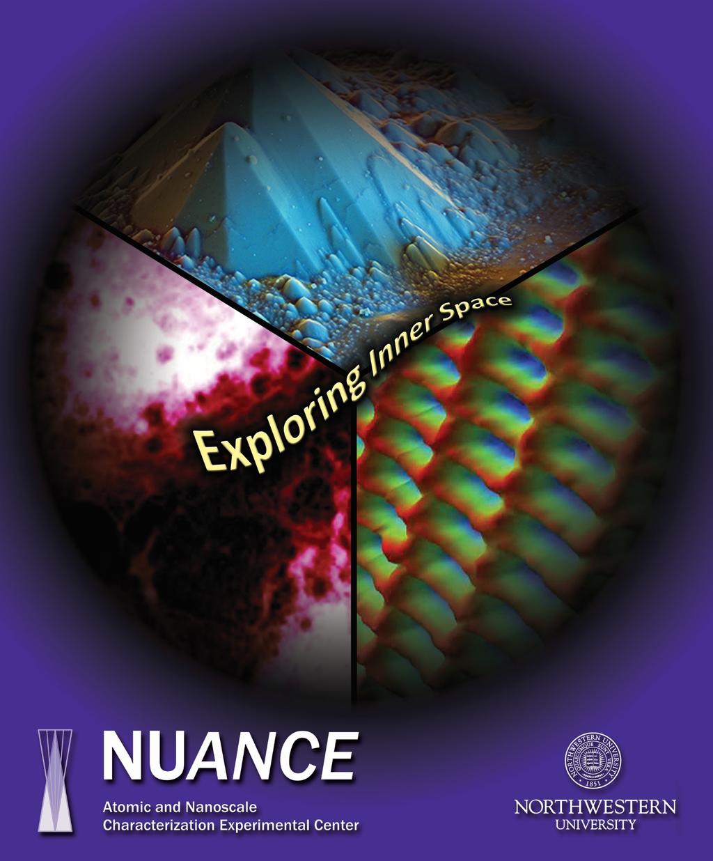
2 The Northwestern University Atomic and Nanoscale Characterization Experimental Center (NUANCE) was established during to integrate complementary analytical instruments and characterization capabilities at Northwestern University. NUANCE serves NU and the broader scientific and engineering community, and provides invaluable resources to the private sector and public institutions in and around the Midwest. An operationally and fiscally efficient solution to the increasing need for advanced analytical and characterization instrumentation, NUANCE leverages staff technical expertise to assist and collaborate with researchers in the physical sciences, engineering, and interdisciplinary fields. NUANCE integrates three complementary instrumentation facilities: EPIC, Keck-II, and SPID under a unified management umbrella. These three facilities are a unique, centralized and comprehensive resource for the NU community and beyond. NUANCE retains the individual identity of the three facilities, but their integration with unified operations promotes synergy among instruments, staff, training, service, technical expertise and new cross-disciplinary initiatives. Our mission is to provide and continually update state-of-the-art and core analytical characterization instrumentation resources, with 24/7 open access, for the NU community and beyond. The word resource includes not only mere instrumentation and access, but also hands-on training, education, research collaboration and outreach. NUANCE aspires to be a pro-active and integral part of all scholarly activities related to characterization at and beyond NU.


3 NUANCE actively participates in societal and global outreach, innovative course and curricula development, and hands on laboratory access for students, researchers, staff and faculty. NUANCE serves as an anchor for NU global programs and contributes to international collaborations through the exchange of researchers and students. NUANCE is renowned for developing a welltrained and globally informed workforce in interdisciplinary science and technology. Local teachers, museums, and members of the community are encouraged to join NUANCE through open house visits, demonstrations, and online. EPIC: Electron Probe Instrumentation Center Keck-II: Keck Interdisciplinary Surface Science Center SPID: Scanned Probe Imaging and Development Facility
 houses an array of scanning, transmission and scanning")

 FEI Vitrobot Plunge Freezer Leica UC7/FC7 Cryo-")

 Electron Energy Loss Spectroscopy (EELS) Bright-Field and")
 with Annular Bright-Field, Dark-Field, and High-Angle")
 Simultaneous SEM and STEM Imaging at 200keV TEM and")
 System Energy")
4 Formed under the NU Materials Research Center (MRC), the Electron Probe Instrumentation Center (EPIC) houses an array of scanning, transmission and scanning transmission electron microscopes (SEM, TEM and STEM), a comprehensive specimen preparation facility, and a BioCryo Facility for imaging and analysis of biological and soft samples. High Pressure Freezer HPM100 (Leica) FEI Vitrobot Plunge Freezer Leica UC7/FC7 Cryo- Ultramicrotome Hitachi HT-7700 S/TEM Hitachi HD-2300 Dual EDS Cryo STEM Hitachi H-8100 TEM Leica EM ACE 600 JEOL JEM-2100F FasTEM EPIC BIOCRYO, TEM & STEM CAPABILITIES SE-, TE-, and Z-Contrast Imaging Electron Diffraction Energy Dispersive X-Ray Spectroscopy (EDS) Electron Energy Loss Spectroscopy (EELS) Bright-Field and Dark-Field Imaging High Resolution Electron Microscopy (HREM) Scanning Transmission Electron Microscopy (STEM) with Annular Bright-Field, Dark-Field, and High-Angle Annular Dark-Field Detectors Selected Area Electron Diffraction (SAED) Convergent Beam Electron Diffraction (CBED) Simultaneous SEM and STEM Imaging at 200keV TEM and STEM Electron Tomography Cryo (Liquid Nitrogen) S/TEM Imaging In Situ Heating, Fluid-Flow, and Electric Biasing TEM/STEM Gatan Image Filter (GIF) System Energy Filtered Transmission Electron Microscopy (EFTEM) Nano Beam Diffraction and Convergent Beam Electron Diffraction (CBED)


")
")

")


5 Hitachi S3400N-II SEM Hitachi S4800-II cfeg SEM Hitachi SU8030 cfeg SEM LEO Gemini 1525 SEM FEI Quanta 600F ESEM FEI Helios Nanolab 600 Dual Beam EPIC SEM CAPABILITIES X-Ray Microanalysis (EDS) Electron Backscatter Diffraction (EBSD) Cathodoluminescence (CL) Electron Beam Lithography Ion Beam Nanofabrication Environmental SEM (ESEM) Focused Ion Beam (FIB) Tomography Ultra-High Resolution Imaging In Situ Nanomanipulation and Probing SE and BSE Imaging STEM Imaging Cryo SEM Imaging Site-Specific Sample Preparation EPIC SAMPLE PREPARATION CAPABILITIES Precise Cutting, Grinding and Polishing Chemical Etching Ion Beam Thinning Spin, Sputter, and Os Coating Metal and Carbon Evaporation High-Pressure Freezing Critical Point and Freeze Drying Cryo Plunging and Transfer System Plasma and UV Cleaning Resin Embedding Cryo Ultramicrotomy


")


 X-ray")
")


6 Keck-II was established through the support of the W. M. Keck Foundation. It houses state-of-the-art surface analysis and related instrumentation. High Resolution Stylus Profilometer 3D Optical Microscope Confocal Raman Spectroscopy Fourier Transform Infrared (FT-IR) Spectroscopy Spectroscopic Ellipsometer Time-of-Flight Secondary Ion Mass Spectrometry (ToF- SIMS) X-ray Photoelectron Spectroscopy (XPS/ESCA) Zetasizer KECK-II CAPABILITIES High Resolution XPS XPS Imaging UPS Depth Profiling ToF-SIMS Spectroscopy, Mapping, Depth Profiling FT-IR ATR PM-IRRAS Surface Profiling Spectroscopic Ellipsometry Confocal Raman Spectroscopy Photoluminescence Zeta Potential and Particle Size
 Facility was")


7 The Scanned Probe Imaging and Development (SPID) Facility was established under the leadership of the International Institute for Nanotechnology (IIN), primarily through funding support from the State of Illinois. SPID provides state-of-the-art soft lithographic patterning, atomic and molecular quantitative imaging and analysis capabilities. HORIBA LabRAM HR Evolution Confocal RAMAN System Bruker BioScope Catalyst Hysitron 950 Triboindenter Bruker Dimension ICON PT System Bruker Dimension FastScan AFM SPID CAPABILITIES Scanning Kelvin Probe Microscopy Fluorescent and Collection Mode Imaging Multiplexed Biomaterials Nanopatterining Low and High Temperature Capabilities Dynamic Modulus and Quantitative Current Mapping Fastscan and Electrochemical AFM Peak Fore TUNA and Conducting AFM Nanoman Aqueous Ambient, Viscoelastic, Quantitative Nanomechnical, Life Science, Phase Contrast, Piezoresponse, and Brightfield and Darkfield Imaging Combined Optical, Fluorescent and AFM Imaging Scratch Testing Nano-Indentation of Soft and Hard Materials High Speed Imaging

8 Technical Inquiries: Prof. Vinayak P. Dravid Director, NUANCE Center Financial Operations: Outreach and Education: Chad Goeser Raymond Bailey Financial Administrator, NUANCE Center Outreach Coordinator, NUANCE Center
NUANCE Center. Northwestern University Atomic and Nanoscale Experimental Characterization Center. Professor Vinayak P. Dravid, Ph.D.
 NUANCE Center Northwestern University Atomic and Nanoscale Experimental Characterization Center Professor Vinayak P. Dravid, Ph.D. Director NUANCE CENTER NU Atomic and Nanoscale Characterization Experimental
ELECTRON MICROSCOPE UNIT
 ELECTRON MICROSCOPE Director: Prof Richard Tilley Associate Director: Dr Nicholas Ariotti Lab Manager: Ms Katie Levick Administrative Assistant: Mr Michael Zhi UNIT Basement Level: F10 Chemical Sciences
Preamble: Emphasis: Material = Device? MTSE 719 PHYSICAL PRINCIPLES OF CHARACTERIZATION OF SOLIDS
 MTSE 719 PHYSICAL PRINCIPLES OF CHARACTERIZATION OF SOLIDS MTSE 719 - PHYSCL PRIN CHARACTIZTN SOLIDS Section # Call # Days / Times 001 96175 -View Book Info - F:100PM - 355PM - TIER114 Preamble: Core course
The Illinois MRSEC: Mechanics and Dynamics in Nanodevices
 The Illinois MRSEC: Mechanics and Dynamics in Nanodevices NSF Materials Research Science and Engineering Centers 50-year history 20 Centers, each 2-3 research groups 6 years funding, $2.4 $3.6 million
Dual Beam Helios Nanolab 600 and 650
 Dual Beam Helios Nanolab 600 and 650 In the Clean Room facilities of the INA LMA, several lithography facilities permit to pattern structures at the micro and nano meter scale and to create devices. In
In-Situ Combination of TOF-SIMS and EDS Analysis During FIB Sectioning
 In-Situ Combination of TOF-SIMS and EDS Analysis During FIB Sectioning V. Ray 1, E. Principe 2, T. Piper 2 vray@umd.edu 1. AIM Lab University of Maryland Nanocenter, College Park, MD 2. Tescan USA, Warrendale
The New TEM facility at LCI, KSU. Min Gao Liquid Crystal Institute Kent State University
 The New TEM facility at LCI, KSU Min Gao Liquid Crystal Institute Kent State University 1 Questions to be answered How does TEM work? Why thin specimen? How to prepare one? What is the TEM at LCI like?
An environment designed for success
 An environment designed for success The nanofab is a centralized, open-access, training, service, and collaboration facility, focused on academic research and industrial applications in micro- and nanoscale
Clark Atlanta University Center for Surface Chemistry and Catalysis Instrument Capabilities
 Center for Surface Chemistry and Catalysis Instrument Capabilities For information contact: Dr. Eric Mintz Research Center for Science and Technology Clark Atlanta University Atlanta, Georgia 30314 Phone:
Supporting Information for
 Supporting Information for Au@MoS 2 Core-shell Heterostructures with Strong Light-Matter Interactions Yuan Li,, Jeffrey D. Cain,, Eve D. Hanson,, Akshay A. Murthy,, Shiqiang Hao, Fengyuan Shi,, Qianqian
Chapter 9. Electron mean free path Microscopy principles of SEM, TEM, LEEM
 Chapter 9 Electron mean free path Microscopy principles of SEM, TEM, LEEM 9.1 Electron Mean Free Path 9. Scanning Electron Microscopy (SEM) -SEM design; Secondary electron imaging; Backscattered electron
Supporting Information
 Supporting Information High Performance Electrocatalyst: Pt-Cu Hollow Nanocrystals Xiaofei Yu, a Dingsheng, a Qing Peng a and Yadong Li* a a Department of Chemistry, Tsinghua University, Beijing, 100084
User Fees for the 4D LABS Characterization Facility
 User Fees for the 4D LABS Characterization Facility 1. Imaging Fees Service SEM 1 - Helios: SEM/EDS mode SEM/EDS mode with FIB functions Cryo mode setup SEM 2 Nova NanoSEM SEM/EDS mode SEM/EDS mode with
Supporting Information
 Supporting Information A Low-Temperature Solid-Phase Method to Synthesize Highly Fluorescent Carbon Nitride Dots with Tunable Emission Juan Zhou, Yong Yang, and Chun-yang Zhang* Single-Molecule Detection
Shared Experimental Facilities Your Partner for Materials Characterization at the University of California, Santa Barbara
 Shared Experimental Facilities Your Partner for Materials Characterization at the University of California, Santa Barbara MATERIALS RESEARCH LABORATORY AT UCSB: AN NSF MRSEC Shared Experimental Facilities
8:30 am 5:00 pm Sunday Short Courses X10 - Exploring Cryo-Preparation Techniques for Biological Samples. X11 - Advanced Focused Ion Beam Methods
 Friday, August 3 8:30 am MSA Council Saturday, August 4 8:30 am MSA Council 8:30 am 5:00 pm Pre-Meeting Congress X60 - Pre-Meeting Congress for Early Career Professionals in Microscopy & Microanalysis
Applications of XPS, AES, and TOF-SIMS
 Applications of XPS, AES, and TOF-SIMS Scott R. Bryan Physical Electronics 1 Materials Characterization Techniques Microscopy Optical Microscope SEM TEM STM SPM AFM Spectroscopy Energy Dispersive X-ray
CHARACTERIZATION of NANOMATERIALS KHP
 CHARACTERIZATION of NANOMATERIALS Overview of the most common nanocharacterization techniques MAIN CHARACTERIZATION TECHNIQUES: 1.Transmission Electron Microscope (TEM) 2. Scanning Electron Microscope
Supplementary Information:
 Supplementary Information: One-Step and Rapid Synthesis of Clean and Monodisperse Dendritic Pt Nanoparticles and Their High Performance Toward Methanol Oxidation and p-nitrophenol Reduction Jun Wang, Xin-Bo
Characterisation of Catalysts Using Secondary and Backscattered Electron In-lens Detectors
 Platinum Metals Rev., 2014, 58, (2), 106 110 FINAL ANALYSIS Characterisation of Catalysts Using Secondary and Backscattered Electron In-lens Detectors Heterogeneous catalysis often involves the use of
Nanoscale Chemical Characterization: Moving to 3 Dimensions
 Nanoscale Chemical Characterization: Moving to 3 Dimensions Eric B. Steel Chemical Science & Technology Laboratory National Institute of Standards & Technology Outline What is and why do we need chemical
Programme for WEM2011. Time Title of the talk Code Presenting Author. Day 0: Tuesday, November 22, 2011
 Programme for WEM2011 Time Title of the talk Code Presenting Author Day 0: Tuesday, November 22, 2011 20:00 21:30: Dinner for Outstation (non-local) Participants at the Hotel Suryansh Day 1: Wednesday,
Microscopy: Principles
 Low Voltage Electron Microscopy: Principles and Applications Edited by David C. Bell Harvard University, USA and Natasha Erdman JEOL USA Inc., USA Published in association with the Royal Microscopical
Opportunities for Advanced Plasma and Materials Research in National Security
 Opportunities for Advanced Plasma and Materials Research in National Security Prof. J.P. Allain allain@purdue.edu School of Nuclear Engineering Purdue University Outline: Plasma and Materials Research
Supporting Information s for
 Supporting Information s for # Self-assembling of DNA-templated Au Nanoparticles into Nanowires and their enhanced SERS and Catalytic Applications Subrata Kundu* and M. Jayachandran Electrochemical Materials
HOW TO APPROACH SCANNING ELECTRON MICROSCOPY AND ENERGY DISPERSIVE SPECTROSCOPY ANALYSIS. SCSAM Short Course Amir Avishai
 HOW TO APPROACH SCANNING ELECTRON MICROSCOPY AND ENERGY DISPERSIVE SPECTROSCOPY ANALYSIS SCSAM Short Course Amir Avishai RESEARCH QUESTIONS Sea Shell Cast Iron EDS+SE Fe Cr C Objective Ability to ask the
Techniques EDX, EELS et HAADF en TEM: possibilités d analyse et applications
 Techniques EDX, EELS et HAADF en TEM: possibilités d analyse et applications Thomas Neisius Université Paul Cézanne Plan Imaging modes HAADF Example: supported Pt nanoparticles Electron sample interaction
Scanning Electron Microscopy
 Scanning Electron Microscopy Amanpreet Kaur 1 www.reading.ac.uk/emlab Scanning Electron Microscopy What is scanning electron microscopy? Basic features of conventional SEM Limitations of conventional SEM
CBE Science of Engineering Materials. Scanning Electron Microscopy (SEM)
") CBE 30361 Science of Engineering Materials Scanning Electron Microscopy (SEM) Scale of Structure Organization Units: micrometer = 10-6 m = 1µm nanometer= 10-9 m = 1nm Angstrom = 10-10 m = 1Å A hair is
CBE 30361 Science of Engineering Materials Scanning Electron Microscopy (SEM) Scale of Structure Organization Units: micrometer = 10-6 m = 1µm nanometer= 10-9 m = 1nm Angstrom = 10-10 m = 1Å A hair is
CURRICULUM VITAE. Department of Physics (D.P), College of Science (C.S), Sudan University of Science and
, College of Science (C.S), Sudan University of Science and") CURRICULUM VITAE DATE: July 2016 PERSONAL DATA: NAME: Abd Ellateef Abbass Abd Ellateef Mohammed Khair (AE. Abbass) NATIONALITY: Sudanese GENDER: Male PLACE AND DATE OF BIRTH: Sudan, 02 / May / 1977 LANGUAGES:
CURRICULUM VITAE DATE: July 2016 PERSONAL DATA: NAME: Abd Ellateef Abbass Abd Ellateef Mohammed Khair (AE. Abbass) NATIONALITY: Sudanese GENDER: Male PLACE AND DATE OF BIRTH: Sudan, 02 / May / 1977 LANGUAGES:
Supporting Information. Synthesis of Mg/ Al Layered Double Hydroxides for Adsorptive Removal of. Fluoride from Water: A Mechanistic and Kinetic Study
 Supporting Information Synthesis of Mg/ Al Layered Double Hydroxides for Adsorptive Removal of Fluoride from Water: A Mechanistic and Kinetic Study Gautam Kumar Sarma and Md. Harunar Rashid* Department
Metrology is not a cost factor, but a profit center
 Edition February 2018 Semiconductor technology & processing Metrology is not a cost factor, but a profit center In recent years, remarkable progress has been made in the field of metrology, which is crucial
Equipment and Facilities of National Institute for Materials Science
 Equipment and Facilities of National Institute for Materials Science March 9, 2018 The followings are facilities which are provided for shared use to any person who engages in scientific and technological
PHYS-E0541:Special Course in Physics Gas phase synthesis of carbon nanotubes for thin film application. Electron Microscopy. for
 PHYS-E0541:Special Course in Physics Gas phase synthesis of carbon nanotubes for thin film application Electron Microscopy for Introduction to Electron Microscopy Carbon Nanomaterials (nanotubes) Dr. Hua
Introduction to Microscopy. Boonrat Lohwongwatana
 Introduction to Microscopy Boonrat Lohwongwatana boonrat@gmail.com http://ows.public.sembach.af.mil/index.cfm Avoiding stereological bias inherent to the appearance of 3-D objects on
Instantaneous reduction of graphene oxide at room temperature
 Instantaneous reduction of graphene oxide at room temperature Barun Kuma Burman, Pitamber Mahanandia and Karuna Kar Nanda Materials Research Centre, Indian Institute of Science, Bangalore-560012, India
Surface Analytical Techniques for Analysis of Coatings Mary Jane Walzak, Mark Biesinger and Brad Kobe The University of Western Ontario, Surface
 Surface Analytical Techniques for Analysis of Coatings Mary Jane Walzak, Mark Biesinger and Brad Kobe The University of Western Ontario, Surface Science Western 999 Collip Circle, Room LL31, London, ON
Photolithography 光刻 Part II: Photoresists
 微纳光电子材料与器件工艺原理 Photolithography 光刻 Part II: Photoresists Xing Sheng 盛兴 Department of Electronic Engineering Tsinghua University xingsheng@tsinghua.edu.cn 1 Photolithography 光刻胶 负胶 正胶 4 Photolithography
Supporting Information
 Supporting Information Pt Nanoparticles Anchored Molecular Self-Assemblies of DNA: An Extremely Stable and Efficient HER Electrocatalyst with Ultra-Low Pt Content Sengeni Anantharaj, $ Pitchiah E. Karthik,
Description of Postdoc 1:
 Description of Postdoc 1: Postdoctoral Research Associate in Mineral Self-Assembly and Chemical Coupling Applications are invited for a postdoctoral research position (PRA) funded by the ERC Advanced Grant
Gold nanothorns macroporous silicon hybrid structure: a simple and ultrasensitive platform for SERS
 Supporting Information Gold nanothorns macroporous silicon hybrid structure: a simple and ultrasensitive platform for SERS Kamran Khajehpour,* a Tim Williams, b,c Laure Bourgeois b,d and Sam Adeloju a
An Ideal Electrode Material, 3D Surface-Microporous Graphene for Supercapacitors with Ultrahigh Areal Capacitance
 Supporting Information An Ideal Electrode Material, 3D Surface-Microporous Graphene for Supercapacitors with Ultrahigh Areal Capacitance Liang Chang, 1 Dario J. Stacchiola 2 and Yun Hang Hu 1, * 1. Department
Carbon Quantum Dots/NiFe Layered Double Hydroxide. Composite as High Efficient Electrocatalyst for Water
 Supplementary Information Carbon Quantum Dots/NiFe Layered Double Hydroxide Composite as High Efficient Electrocatalyst for Water Oxidation Di Tang, Juan Liu, Xuanyu Wu, Ruihua Liu, Xiao Han, Yuzhi Han,
Electronic Supplementary Information
 Electronic Supplementary Information Facile synthesis of halogenated carbon quantum dots as an important intermediate for surface modification Jin Zhou, Pei Lin, Juanjuan Ma, Xiaoyue Shan, Hui Feng, Congcong
Industry needs: Characterisation & Analysis. Prof. Valeria Nicolosi
 Industry needs: Characterisation & Analysis Prof. Valeria Nicolosi Cleanroom Facility Cleanroom Facility Class 100 and 10,000 cleanroom facility. Cleanroom Sample Preparation Substrates are diced Into
2D Materials Research Activities at the NEST lab in Pisa, Italy. Stefan Heun NEST, Istituto Nanoscienze-CNR and Scuola Normale Superiore, Pisa, Italy
 2D Materials Research Activities at the NEST lab in Pisa, Italy Stefan Heun NEST, Istituto Nanoscienze-CNR and Scuola Normale Superiore, Pisa, Italy 2D Materials Research Activities at the NEST lab in
Supporting Online Material for
 www.sciencemag.org/cgi/content/full/321/5894/1331/dc1 Supporting Online Material for Identification of Active Gold Nanoclusters on Iron Oxide Supports for CO Oxidation Andrew A. Herzing, Christopher J.
Weak-Beam Dark-Field Technique
 Basic Idea recall bright-field contrast of dislocations: specimen close to Bragg condition, s î 0 Weak-Beam Dark-Field Technique near the dislocation core, some planes curved to s = 0 ) strong Bragg reflection
Engineering electronic structure of Two-Dimensional Subnanopore. nanosheet by Molecular Titanium-oxide Incorporation for Enhanced
 Electronic Supplementary Material (ESI) for Chemical Science. This journal is The Royal Society of Chemistry 2015 Electronic Supplementary Information for Engineering electronic structure of Two-Dimensional
Standards for Nanotechnology Workforce Education
 Standards for Nanotechnology Workforce Education Standards Development Organizations (SDOs) Global International Organization for Standardization International Electrotechnical Commission Regional European
MSE 321 Structural Characterization
 Auger Spectroscopy Auger Electron Spectroscopy (AES) Scanning Auger Microscopy (SAM) Incident Electron Ejected Electron Auger Electron Initial State Intermediate State Final State Physical Electronics
X-Ray & Thermal Analysis Unit. Unit Pengurusan Makmal Universiti Blok T03 Bangunan UIRL Universiti Teknologi Malaysia Skudai Johor
 X-Ray & Thermal Analysis Unit Unit Pengurusan Makmal Universiti Blok T03 Bangunan UIRL Universiti Teknologi Malaysia 81310 Skudai Johor Contents Introduction Team Members Laboratory Instrument XPS XRD
Nanoelectronics 09. Atsufumi Hirohata Department of Electronics. Quick Review over the Last Lecture
 Nanoelectronics 09 Atsufumi Hirohata Department of Electronics 13:00 Monday, 12/February/2018 (P/T 006) Quick Review over the Last Lecture ( Field effect transistor (FET) ): ( Drain ) current increases
Supporting Information An Interlaced Silver Vanadium Oxide-Graphene Hybrid with High Structural Stability for Use in Lithium Ion Batteries
 Electronic Supplementary Material (ESI) for ChemComm. This journal is The Royal Society of Chemistry 2014 Supporting Information An Interlaced Silver Vanadium Oxide-Graphene Hybrid with High Structural
Imaging Methods: Scanning Force Microscopy (SFM / AFM)
") Imaging Methods: Scanning Force Microscopy (SFM / AFM) The atomic force microscope (AFM) probes the surface of a sample with a sharp tip, a couple of microns long and often less than 100 Å in diameter.
Imaging Methods: Scanning Force Microscopy (SFM / AFM) The atomic force microscope (AFM) probes the surface of a sample with a sharp tip, a couple of microns long and often less than 100 Å in diameter.
raw materials C V Mn Mg S Al Ca Ti Cr Si G H Nb Na Zn Ni K Co A B C D E F
 Today s advanced batteries require a range of specialized analytical tools to better understand the electrochemical processes that occur during battery cycling. Evans Analytical Group (EAG) offers a wide-range
Remote Access to Hi-tech Equipment
 Remote Access to Hi-tech Equipment From Your Classroom to Ours Sebastien Maeder Outline What is Remote Access? The Method vs. the Goal The role within NACK Why should we try? Confines of Classroom Characterization
ABNORMAL X-RAY EMISSION FROM INSULATORS BOMBARDED WITH LOW ENERGY IONS
 302 ABNORMAL X-RAY EMISSION FROM INSULATORS BOMBARDED WITH LOW ENERGY IONS M. Song 1, K. Mitsuishi 1, M. Takeguchi 1, K. Furuya 1, R. C. Birtcher 2 1 High Voltage Electron Microscopy Station, National
Characterization of Nanomaterials Under the Special Aspect of Migration from Packaging Materials into Food
 Characterization of Nanomaterials Under the Special Aspect of Migration from Packaging Materials into Food Jochen Weiss Workshop on Outlook and Challenges of Nanotechnologies for Food Packaging ILSI, Brussels,
Transmission Electron Microscopy
 L. Reimer H. Kohl Transmission Electron Microscopy Physics of Image Formation Fifth Edition el Springer Contents 1 Introduction... 1 1.1 Transmission Electron Microscopy... 1 1.1.1 Conventional Transmission
Electronic Supplementary Information (ESI)
") Electronic Supplementary Information (ESI) A thin-layered chromatography plate prepared from naphthalimide-based receptor immobilized SiO 2 nanoparticles as a portable chemosensor and adsorbent for Pb
Electronic Supplementary Information (ESI) A thin-layered chromatography plate prepared from naphthalimide-based receptor immobilized SiO 2 nanoparticles as a portable chemosensor and adsorbent for Pb
NTECH - Nanotechnology
 Coordinating unit: Teaching unit: Academic year: Degree: ECTS credits: 2017 230 - ETSETB - Barcelona School of Telecommunications Engineering 710 - EEL - Department of Electronic Engineering 713 - EQ -
MSE 321 Structural Characterization
 Auger Spectroscopy Auger Electron Spectroscopy (AES) Scanning Auger Microscopy (SAM) Incident Electron Ejected Electron Auger Electron Initial State Intermediate State Final State Physical Electronics
2012/01/20. Thierry EPICIER. MATEIS-CLYM, umr CNRS5510, Director METSA (FR 3507 CNRS) M. AOUINE, JP MILLET et al.
 M. AOUINE, JP MILLET et al.") 2012/01/20 Thierry EPICIER MATEIS-CLYM, umr CNRS5510, Director METSA (FR 3507 CNRS) thierry.epicier@insa-lyon.fr M. AOUINE, JP MILLET et al. MATERIALS SCIENCES & NANOTECHNOLOGIES HIGH RESOLUTION MICROSCOPY
2012/01/20 Thierry EPICIER MATEIS-CLYM, umr CNRS5510, Director METSA (FR 3507 CNRS) thierry.epicier@insa-lyon.fr M. AOUINE, JP MILLET et al. MATERIALS SCIENCES & NANOTECHNOLOGIES HIGH RESOLUTION MICROSCOPY
Surface Analysis - The Principal Techniques
 Surface Analysis - The Principal Techniques 2nd Edition Editors johnc.vickerman Manchester Interdisciplinary Biocentre, University of Manchester, UK IAN S. GILMORE National Physical Laboratory, Teddington,
Pd-P nanoalloys supported on porous carbon frame as efficient catalyst for benzyl alcohol oxidation
 Electronic Supplementary Material (ESI) for Catalysis Science & Technology. This journal is The Royal Society of Chemistry 2018 Supporting information Pd-P nanoalloys supported on porous carbon frame as
A highly reactive chalcogenide precursor for the synthesis of metal chalcogenide quantum dots
 Electronic Supplementary Material (ESI) for Nanoscale. This journal is The Royal Society of Chemistry 2015 Electronic supplementary information A highly reactive chalcogenide precursor for the synthesis
Transmission Electron Microscopy. Part #2 High Resolution Imaging XEDS EELS spectroscopies Aberration corrected TEM
 Transmission Electron Microscopy Part #2 High Resolution Imaging XEDS EELS spectroscopies Aberration corrected TEM Nicolas Menguy Institut de Minéralogie, de Physique des Matériaux et de Cosmochimie Part
Chemical Imaging of High Voltage Cathode Interface
 Chemical Imaging of High Voltage Cathode Interface Jigang Zhou Canadian Light Source (CLS) 34 th International Battery Seminar And Exhibit Fort Lauderdale, FL March 20-23, 2017 1 Billion times brighter
MATERIALS CHARACTERIZATION AND TESTING PLATFORM
 service offer MATERIALS CHARACTERIZATION AND TESTING PLATFORM Materials Materials Characterization and Testing Platform LIST's Materials Characterization and Testing Platform supports all Luxembourg and
Scanning Electron Microscopy (SEM) with Energy Dispersive Spectroscopy (EDS) Analysis The samples were also characterized by scanning electron
 with Energy Dispersive Spectroscopy (EDS) Analysis The samples were also characterized by scanning electron") Electronic Supplementary Material (ESI) for RSC Advances. This journal is The Royal Society of Chemistry 2016 Scanning Electron Microscopy (SEM) with Energy Dispersive Spectroscopy (EDS) Analysis The samples
Electronic Supplementary Material (ESI) for RSC Advances. This journal is The Royal Society of Chemistry 2016 Scanning Electron Microscopy (SEM) with Energy Dispersive Spectroscopy (EDS) Analysis The samples
Characterization of zeolites by advanced SEM/STEM techniques
 SCIENTIFIC INSTRUMENT NEWS 2016 Vol. 7 SEPTEMBER Technical magazine of Electron Microscope and Analytical Instruments. Article Characterization of zeolites by advanced SEM/STEM techniques Toshiyuki Yokoi
Advanced Analytical Training
 Advanced Analytical Training Failure Analysis MIMOS Berhad, Technology Park Malaysia 24-26 Apr 2019 Strong knowledge and understanding of failure mechanism especially in semiconductor packaging are some
Facilities, Services and Rates
 Facilities, Services and Rates Our unique facilities are available for public and private research centers as well as for the industry, who will find in the LMA equipment, a unique research capacity and
Enhanced photocurrent of ZnO nanorods array sensitized with graphene. quantum dots
 Electronic Supplementary Material (ESI) for RSC Advances. This journal is The Royal Society of Chemistry 2015 Enhanced photocurrent of ZnO nanorods array sensitized with graphene quantum dots Bingjun Yang,
ToF-SIMS or XPS? Xinqi Chen Keck-II
 ToF-SIMS or XPS? Xinqi Chen Keck-II 1 Time of Flight Secondary Ion Mass Spectrometry (ToF-SIMS) Not ToF MS (laser, solution) X-ray Photoelectron Spectroscopy (XPS) 2 3 Modes of SIMS 4 Secondary Ion Sputtering
A PLATFORM FACILITATING IDEAS AND INNOVATIONS
 Scan here for more information A PLATFORM FACILITATING IDEAS AND INNOVATIONS The SERC (Science and Engineering Research Council) Nano Fabrication, Processing and Characterisation (SnFPC) platform aims
How to Use the Devices in the Analytical Instrument Laboratory
 How to Use the Devices in the Analytical Instrument Laboratory 1. Eligible users To be eligible, the user must be a member of the faculty or staff, a researcher, or a Waseda University student. If the
Leveraging Commercial Silver Inks as Oxidation Reduction Reaction Catalysts in Alkaline Medium
 Supporting Information Leveraging Commercial Silver Inks as Oxidation Reduction Reaction Catalysts in Alkaline Medium Shlomi Polani, Naftali Kanovsky and David Zitoun, *, Bar Ilan University, Department
Supporting Information
 Electronic Supplementary Material (ESI) for Chemical Communications. This journal is The Royal Society of Chemistry 2016 Supporting Information Single-crystalline Pd square nanoplates enclosed by {100}
Technology, Techniques and Applications. Ric Allott Business Development Manager
 Technology, Techniques and Applications Ric Allott Business Development Manager 1 Central Laser Facility ASTRA GEMINI VULCAN ARTEMIS ULTRA OCTOPUS High power, ultrashort pulse dual beams of 15 J, 30 fs
MS482 Materials Characterization ( 재료분석 ) Lecture Note 11: Scanning Probe Microscopy. Byungha Shin Dept. of MSE, KAIST
 Lecture Note 11: Scanning Probe Microscopy. Byungha Shin Dept. of MSE, KAIST") 2015 Fall Semester MS482 Materials Characterization ( 재료분석 ) Lecture Note 11: Scanning Probe Microscopy Byungha Shin Dept. of MSE, KAIST 1 Course Information Syllabus 1. Overview of various characterization
2015 Fall Semester MS482 Materials Characterization ( 재료분석 ) Lecture Note 11: Scanning Probe Microscopy Byungha Shin Dept. of MSE, KAIST 1 Course Information Syllabus 1. Overview of various characterization
TESCAN S New generation of FIB-SEM microscope
 TESCAN S New generation of FIB-SEM microscope rising standards in sample preparation Key Features SEM COLUMN Versatile system for unlimited applications: resolution imaging (0.9 nm at 15 kev, 1.4 nm at
FIELD EMISSION SCANNING ELECTRON MICROSCOPY
 FIELD EMISSION SCANNING ELECTRON MICROSCOPY Make: Carl Zeiss, Germany Model: SUPRA 55VP, Gemini Column. With air lock system Detectors; 1, Secondary Electron 1 (In Lens) 2, Secondary Electron 2(SE2) 3,
Analytical Methods for Materials
 Analytical Methods for Materials Lesson 21 Electron Microscopy and X-ray Spectroscopy Suggested Reading Leng, Chapter 3, pp. 83-126; Chapter 4, pp. 127-160; Chapter 6, pp. 191-219 P.J. Goodhew, J. Humphreys
Crystalline Surfaces for Laser Metrology
 Crystalline Surfaces for Laser Metrology A.V. Latyshev, Institute of Semiconductor Physics SB RAS, Novosibirsk, Russia Abstract: The number of methodological recommendations has been pronounced to describe
Biomimetic Structure Design and Construction of Cactus-like MoS2/Bi19Cl3S27 Photocatalyst for Efficient Hydrogen Evolution
 Electronic Supplementary Material (ESI) for Journal of Materials Chemistry A. This journal is The Royal Society of Chemistry 2018 Electronic Supplementary Information (ESI) Biomimetic Structure Design
Supplementary Information for
 Supplementary Information for Facile transformation of low cost thiourea into nitrogen-rich graphitic carbon nitride nanocatalyst with high visible light photocatalytic performance Fan Dong *a, Yanjuan
Graphene Quantum Dots based systems as HIV. Inhibitors
 Supporting Information to Graphene Quantum Dots based systems as HIV Inhibitors Daniela Iannazzo, *, Alessandro Pistone, Stefania Ferro, Laura De Luca, Anna Maria Monforte, Roberto Romeo, Maria Rosa Buemi
Johnson Matthey, Oxford University and Diamond Light Source to Invest in New Capability for Materials Analysis
 4 th August 2014 Johnson Matthey, Oxford University and Diamond Light Source to Invest in New Capability for Materials Analysis Today Johnson Matthey, Oxford University and Diamond Light Source announce
QUEENSBOROUGH COMMUNITY COLLEGE CHEMISTRY DEPARTMENT. LECTURE: 3 hours per week CREDITS: 3
 QUEENSBOROUGH COMMUNITY COLLEGE CHEMISTRY DEPARTMENT CH-5 H INTRODUCTION TO NANOSCIENCE LECTURE: hours per week CREDITS: TEXTBOOK: Introduction to Nanoscience & Nanotechnology. ISBN: 978-400-4779-0 By
IMAGING DIFFRACTION SPECTROSCOPY
 TEM Techniques TEM/STEM IMAGING DIFFRACTION SPECTROSCOPY Amplitude contrast (diffracion contrast) Phase contrast (highresolution imaging) Selected area diffraction Energy dispersive X-ray spectroscopy
Supporting Information
 Supporting Information Identification of the nearby hydroxyls role in promoting HCHO oxidation over a Pt catalyst Ying Huo #, Xuyu Wang #, Zebao Rui *, Xiaoqing Yang, Hongbing Ji * School of Chemical Engineering
Supplementary information
 Supplementary information Supplementary Figures Supplementary Figure 1. CO 2 light off curve obtained from the 5 wt% Pt/Al 2 O 3 catalyst obtained through heating the catalyst under a 50 ml.min -1 flow
Electron Microscopy & Spectroscopy: Window to the Nanoworld!
 Electron Microscopy & Spectroscopy: Window to the Nanoworld! Vinayak P. Dravid Professor, Materials Science & Engineering Director, NUANCE Center Institute for Nanotechnology Northwestern University Evanston,
City University of Hong Kong. Course Syllabus. offered by Department of Physics and Materials Science with effect from Semester A 2016 / 17
 City University of Hong Kong offered by Department of Physics and Materials Science with effect from Semester A 2016 / 17 Part I Course Overview Course Title: Nanostructures and Nanotechnology Course Code:
EDS User School. Principles of Electron Beam Microanalysis
 EDS User School Principles of Electron Beam Microanalysis Outline 1.) Beam-specimen interactions 2.) EDS spectra: Origin of Bremsstrahlung and characteristic peaks 3.) Moseley s law 4.) Characteristic
Controlled self-assembly of graphene oxide on a remote aluminum foil
 Supplementary Information Controlled self-assembly of graphene oxide on a remote aluminum foil Kai Feng, Yewen Cao and Peiyi Wu* State key Laboratory of Molecular Engineering of Polymers, Department of
MODERN TECHNIQUES OF SURFACE SCIENCE
 MODERN TECHNIQUES OF SURFACE SCIENCE Second edition D. P. WOODRUFF & T. A. DELCHAR Department ofphysics, University of Warwick CAMBRIDGE UNIVERSITY PRESS Contents Preface to first edition Preface to second
Role of Re and Ru in Re Ru/C Bimetallic Catalysts for the
 Role of Re and Ru in Re Ru/C Bimetallic Catalysts for the Aqueous Hydrogenation of Succinic Acid Xin Di a, Chuang Li a, Bingsen Zhang b, Ji Qi a, Wenzhen Li c, Dangsheng Su b, Changhai Liang a, * a Laboratory