Supporting Information for
|
|
|
- Daisy Sparks
- 5 years ago
- Views:
Transcription
1 Supporting Information for 2 Core-shell Heterostructures with Strong Light-Matter Interactions Yuan Li,, Jeffrey D. Cain,, Eve D. Hanson,, Akshay A. Murthy,, Shiqiang Hao, Fengyuan Shi,, Qianqian Li,, Chris Wolverton, Xinqi Chen, *,, Vinayak P Dravid *,,, Department of Materials Science and Engineering, Northwestern University Atomic and Nanoscale Characterization Experimental (NUANCE) Center, and International Institute for Nanotechnology (IIN), Northwestern University, Evanston, Illinois 60208, USA *Corresponding author Xinqi Chen: xchen@northwestern.edu Vinayak P Dravid: v-dravid@northwestern.edu 1
2 S1. Experimental details S1.1. Materials and methods Molybdenum trioxide and Sulfur powders were purchased from Alfa Aesar (ward Hill, MA). Galvanic deposition solution contains 1 mm KAuCl 4 and 1% HF. Buffered oxide etch (BOE) was self-prepared by mixing 40% NH 4 F and 49% HF with a volume rate of 6:1. Chemical vapor deposition was conducted in a Lindberg Blue M tube furnace. Heidelberg µpg 501 Maskless Aligner was used for the lithography preparation of Au@MoS 2 patterns on Si substrate as well as the fabrication of photodetector devices. Raman spectra and photoluminescence spectra was collected on the HORIBA LabRAM HR Evolution Confocal Raman System. Electric test was conducted on the Signatone S-1160 Probe Station. X-ray photoelectron spectroscopy (XPS, Thermo Scientific ESCALAB 250Xi) was used for binding energy analysis. Hitachi SU8030 SEM and JEOL JEM-2100 Fas TEM were used for morphological and structural characterizations. S1.2. Chemical vapor deposition of Au@MoS 2 Silicon substrate was cleaned with BOE for 15 s to remove surface oxide layer. This was followed by putting the substrate in above galvanic deposition solution for 60 s to deposit Au film, which was further annealed at 850 C for 15 min to form Au nanoparticles. The following fullerene-like MoS 2 shell encapsulation on Au nanoparticles was conducted via a modified chemical vapor deposition process. Briefly, the Au nanoparticle-coated substrate was put face down on an alumina boat containing 10 mg MoO 3. Another boat containing 120 mg sulfur powders was put in the upstream side. N 2 gas with a flow rate of 200 sccm was used as the 2
3 carrier gas. The furnace was first heated up to 300 C and kept for 30 min, and then ramped to the growth temperature (650 C). The growth was continued for 15 min with a N 2 flow rate of 10 sccm. The furnace was then slowly cooled down to ambient temperature. S1.3. Fabrication of NU Patterns of Au@MoS 2 heterostructures Designed patterns of Au@MoS 2 were fabricated using a standard photolithography process. Briefly, photoresist (S1813) was first coated on silicon substrate with a spin rate of 4000 rpm for 30 s. The substrate was baked at 110 C for 1 min. UV light exposure was conducted for 26 ms with a defocus of -1. The sample was then developed in MF-319 for 30 s and further cleaned with O 2 /Ar plasma for 3 min. Subsequently, an Au film of 10 nm was evaporated on the substrate and the remaining photoresist was removed in acetone. The obtained Au film patterns was annealed at 850 C for 15 min and subjected to the same chemical vapor deposition process as above to form Au@MoS 2 patterns. The obtained patterns at various fabrication steps can be found in Figure S3. S1.4. Discrete Dipole Approximation (DDA) modeling The computation of absorbance and surface electric field distribution of isolated targets (Au nanoparticle, Au@MoS 2 heterostructure, and imaginary MoS 2 shell, see Figure 3D-F) were performed using the Discrete Dipole Approximation algorithm implemented in the DDSCAT 7.2 code developed by Draine and Flatau. 1 The Au nanoparticle target has a diameter of 50 nm. The Au@MoS 2 heterostructure target is composed of an Au nanoparticle core of 50 nm and a MoS 2 shell of 6.5 nm (10 atomic layers of MoS 2 ). The imaginary MoS 2 shell target is same with the 3
4 2 heterostructure target but with no Au core. These targets were built as a lattice of polarizable cubic elements or dipoles with position r i and possibility α i (i = 1, 2,, N). In the simulation, the targets were excited by a monochromatic incident wave vertical to the crosssection of the heterostructures, and the induced extinction and absorption of the targets were calculated by = { } (1) here * represents complex conjugate, = is the wave number of the incident wave and E 0 is its amplitude, E loc,i is the local field calculated from the sum of the incident radiation field of dipole i and the filed radiated by the other N-1 dipoles, and P i is the polarization induced in dipole i, expressed as =,. (2) The absorption efficiency (Q abs ) of the simulated targets (Figure 5A) were calculated from = / (3) where a eff is the effective radius of a sphere with volume ( ) equal to the volume of the heterostructured targets. As mentioned, the strong light-matter interaction at the visible region leads to the generation of SPR, which further forms a constant localized electric field on/near the surface of the targets. 2 The intensity of electric filed was theoretically calculated from the sum of the incident radiation field of dipole i and the filed radiated by the other N-1 dipoles, as shown in the following equation,, =, +, = exp. (4) 4
5 The interaction matrix A can be represented as = + 3 =1,2,,, (5) where = and P is the polarization vector. S1.5. Density functional theory calculation Density functional theory (DFT) electronic structure calculations were performed in order to gain insights into the various band alignments in these materials. The calculations were performed using the generalized gradient approximation with PBE 3 functional for the exchange correlation functional and projector augmented wave potentials as implemented in VASP (Vienna Ab-initio Simulation Package). 4 All structures are fully relaxed with respect to cell vectors and cellinternal positions. The electronic DOS (density of states) is calculated from the relaxed structures using the tetrahedron method with Blöchl corrections. To get the Fermi level relative to the vacuum level of Au, we use 6-layer slab of fcc Au in (111) direction with 15 Angstrom vacuum in the super cell to calculate work function. The work functions of different MoS 2 cases are also calculated to align with Au (111). To approve the relative band alignments of MoS 2 systems, we also utilize the findings of Van de Walleand and Neugebauer, who demonstrated a universal alignment of the electronic transition level of hydrogen in a wide range of materials including semiconductors, insulators and even aqueous solutions. 5 Hence, to infer the band alignment, we compute the energies of H defects in the rock salt compounds of interest, assume alignment between these H energies, and then extract the band alignment of the compounds. To align the valance band maximum position of each system, we consider the defect formation energies of 5
6 various charge states of interstitial Hq (q = -1, 0, 1) by placing H in the host material, calculating the total energy of this structure, and subtracting the energy of the corresponding pure host material, hydrogen chemical potential, and electron chemical potential: 5 = , where E V and E F are valence band maximum and Fermi level (relative to the VBM). To select the most favorable interstitial H binding sites in host materials, multiple binding configurations are calculated. The electrostatic potential correction term E is calculated by inspecting the potential in the supercell far from the impurity and aligning it with the electrostatic potential in bulk. 6 References 1. Draine, B. T., Flatau, P. J. (2013). User guide for the discrete dipole approximation code DDSCAT 7.3. arxiv preprint arxiv: Wu, J.; Shi, W.; Chopra, N. Optical properties of gold/multilayer-graphene/carbon nanotube hybrid materials. Carbon 2014, 68, Perdew, J. P.; Burke, K.; Ernzerhof, M. Generalized Gradient Approximation Made Simple. Phys. Rev. Lett. 1996, 77, Kresse, G.; Furthmüller, Efficient iterative schemes for ab initio total-energy calculations using a plane-wave basis set. J. Phys. Rev. B 1996, 54, Van de Walle, C. G.; Neugebauer, J. Universal alignment of hydrogen levels in semiconductors, insulators and solutions. Nature 2003, 423,
7 6. Van de Walle, C. G.; Neugebauer, J. First-principles calculations for defects and impurities: Applications to III-nitrides. J. Appl. Phys. 2004, 95,385. 7


 SEM images of")
 SEM")
8 S2. Supplementary Figures Figure S1. Formation and dispersion of Au nanoparticles on Si substrate. (a) Schematic showing the galvanic deposition of Au film and its subsequent annealing to form dewetted Au nanoparticles. (b,c) SEM images of the as-deposited Au film. (d,e) SEM images of the annealed Au nanoparticles. a b d c e 8


")


9 Figure S2. EDS line profile of 2. (a) TEM image of a Au@MoS 2 heterostructure. (b) EDS line profiles marked on the Au@MoS 2 heterostructure. (c) Count-position curves of different elements corresponding to various EDS lines across the yellow line in (b). a b c 9

 Optical image and")

 NU patterns after")
 Growth of Au@MoS 2")


 Growth of Au@MoS 2")

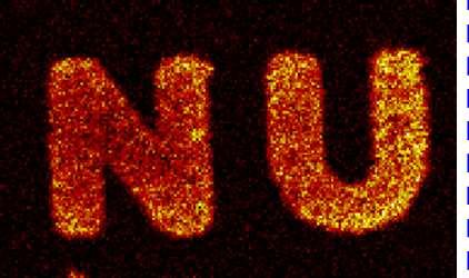
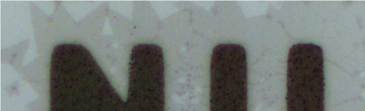
10 Figure S3. Fabrication process of 2 patterns. (a) Optical image and (b) SEM image of NU patterns after galvanic deposition. (c) NU patterns after annealing. (d) Growth of 2 heterostructures on the NU patterns. (e) Optical image of circular patterns with diameter of 10 µm. (f) Growth of 2 using patterns in (e). a Pattern 1 b Au film c Au nanoparticles 50 µm 10 µm 10 µm e Pattern 2 d 50 µm f 10

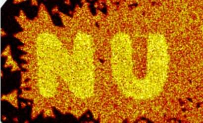
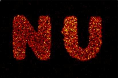

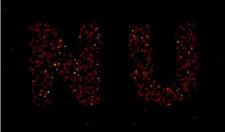

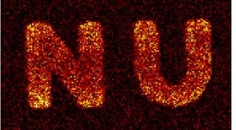
11 Figure S4. SIMS demonstration of the 2 patterns. (a) Optical image of various NU at the edge region of Si substrate. (b-e) SIMS elemental mapping (including Mo, S, and Au) on various patterns. a 50 b c d E Mo Mo Mo Mo S S S S Au Au Au Au 11
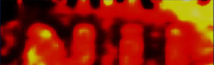
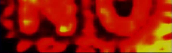

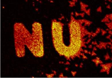
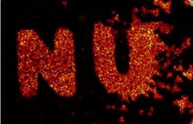
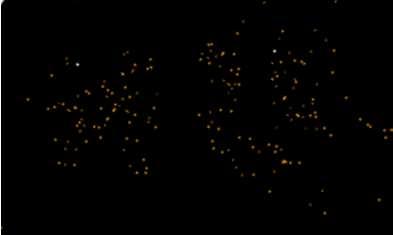
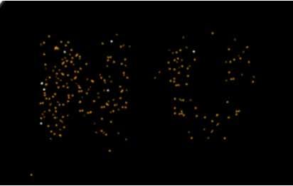
12 Figure S5. Photoluminescence mapping on various 2 patterns. (a,b) photoluminescence mapping with relatively low resolution on another NU patterns. (c,d) NU patterns at the center region of the substrate. a c 10 µm 10 b d 12
 Atomic structure of MoS 2 nanosheet used for the DFT calculation. The x-y coordinate shows the direction for structural bending.")

13 Figure S6. Density functional theory modeling of electronic structure. (a) Band structure of 6-layer MoS 2 flat nanosheet. (b) Atomic structure of MoS 2 nanosheet used for the DFT calculation. The x-y coordinate shows the direction for structural bending. (c) Schematic diagram of band alignment of Au and various MoS 2 systems relative to the vacuum energy level. For energy levels of MoS 2 from left to right, they are respectively pure 6-layer MoS 2 slab, a bent MoS 2 in x, y and xy directions to mimic curved shell structure on Au particles. Here the bent structure refers a curve slab with 5 center angle. All numbers are in ev. The black dashed lines are Fermi levels. a b c 13
Supporting Information
 Electronic Supplementary Material (ESI) for Chemical Science. This journal is The Royal Society of Chemistry 217 Supporting Information Experimental Section Materials. Dicyandiamide(DCDA, C 2 H 4 N 4,
Molybdenum compound MoP as an efficient. electrocatalyst for hydrogen evolution reaction
 Electronic Supplementary Material (ESI) for Energy & Environmental Science. This journal is The Royal Society of Chemistry 2014 Molybdenum compound MoP as an efficient electrocatalyst for hydrogen evolution
Curvature-enhanced Spin-orbit Coupling and Spinterface Effect in Fullerene-based Spin Valves
 Supplementary Information Curvature-enhanced Spin-orbit Coupling and Spinterface Effect in Fullerene-based Spin Valves Shiheng Liang 1, Rugang Geng 1, Baishun Yang 2, Wenbo Zhao 3, Ram Chandra Subedi 1,
Iodine-Mediated Chemical Vapor Deposition Growth of Metastable Transition Metal
 Supporting Information Iodine-Mediated Chemical Vapor Deposition Growth of Metastable Transition Metal Dichalcogenides Qiqi Zhang,, Yao Xiao, #, Tao Zhang,, Zheng Weng, Mengqi Zeng, Shuanglin Yue, ± Rafael
Supplementary Information
 Electronic Supplementary Material (ESI) for Physical Chemistry Chemical Physics. This journal is the Owner Societies 2015 Supplementary Information Vertical Heterostructures of MoS2 and Graphene Nanoribbons
Facet engineered Ag 3 PO 4 for efficient water photooxidation
 Supporting Information Facet engineered Ag 3 PO 4 for efficient water photooxidation David James Martin, Naoto Umezawa, Xiaowei Chen, Jinhua Ye and Junwang Tang* This file includes the following experimental/theoretical
Supporting Information Tuning Local Electronic Structure of Single Layer MoS2 through Defect Engineering
 Supporting Information Tuning Local Electronic Structure of Single Layer MoS2 through Defect Engineering Yan Chen, 1,2,,$, * Shengxi Huang, 3,6, Xiang Ji, 2 Kiran Adepalli, 2 Kedi Yin, 8 Xi Ling, 3,9 Xinwei
Hopping in CVD Grown Single-layer MoS 2
 Supporting Information for Large Thermoelectricity via Variable Range Hopping in CVD Grown Single-layer MoS 2 Jing Wu 1,2,3, Hennrik Schmidt 1,2, Kiran Kumar Amara 4, Xiangfan Xu 5, Goki Eda 1,2,4, and
Covalent Nitrogen Doping and Compressive Strain
 Covalent Nitrogen Doping and Compressive Strain in MoS2 by Remote N2 Plasma Exposure Supplementary Information Angelica Azcatl 1, Xiaoye Qin 1, Abhijith Prakash 2, Chenxi Zhang 1, Lanxia Cheng 1, Qingxiao
Supplementary Information for
 Supplementary Information for Facile transformation of low cost thiourea into nitrogen-rich graphitic carbon nitride nanocatalyst with high visible light photocatalytic performance Fan Dong *a, Yanjuan
Supplementary Figure 1. HRTEM images of PtNi / Ni-B composite exposed to electron beam. The. scale bars are 5 nm.
 Supplementary Figure 1. HRTEM images of PtNi / Ni-B composite exposed to electron beam. The scale bars are 5 nm. S1 Supplementary Figure 2. TEM image of PtNi/Ni-B composite obtained under N 2 protection.
Supporting information. Origins of High Electrolyte-Electrode Interfacial Resistances in Lithium Cells. Containing Garnet Type LLZO Solid Electrolytes
 Electronic Supplementary Material (ESI) for Physical Chemistry Chemical Physics. This journal is the Owner Societies 2014 Supporting information Origins of High Electrolyte-Electrode Interfacial Resistances
Supplementary Figure 1 Detailed illustration on the fabrication process of templatestripped
 Supplementary Figure 1 Detailed illustration on the fabrication process of templatestripped gold substrate. (a) Spin coating of hydrogen silsesquioxane (HSQ) resist onto the silicon substrate with a thickness
The design of an integrated XPS/Raman spectroscopy instrument for co-incident analysis
 The design of an integrated XPS/Raman spectroscopy instrument for co-incident analysis Tim Nunney The world leader in serving science 2 XPS Surface Analysis XPS +... UV Photoelectron Spectroscopy UPS He(I)
UTC Power, South Windsor, CT United Technologies Research Center, East Hartford, CT
 Supporting Information Electrocatalysis on Platinum Nanoparticles: Particle Size Effect on Oxygen Reduction Reaction Activity Minhua Shao,, * Amra Peles,, * Krista Shoemaker UTC Power, South Windsor, CT
Supporting Information
 Copyright WILEY-VCH Verlag GmbH & Co. KGaA, 69469 Weinheim, Germany, 2018. Supporting Information for Small, DOI: 10.1002/smll.201801523 Ultrasensitive Surface-Enhanced Raman Spectroscopy Detection Based
Supplementary Information Our InGaN/GaN multiple quantum wells (MQWs) based one-dimensional (1D) grating structures
 based one-dimensional (1D) grating structures") Polarized white light from hybrid organic/iii-nitrides grating structures M. Athanasiou, R. M. Smith, S. Ghataora and T. Wang* Department of Electronic and Electrical Engineering, University of Sheffield,
Polarized white light from hybrid organic/iii-nitrides grating structures M. Athanasiou, R. M. Smith, S. Ghataora and T. Wang* Department of Electronic and Electrical Engineering, University of Sheffield,
SUPPLEMENTARY FIGURES
 1 SUPPLEMENTARY FIGURES Supplementary Figure 1: Initial stage showing monolayer MoS 2 islands formation on Au (111) surface. a, Scanning tunneling microscopy (STM) image of molybdenum (Mo) clusters deposited
Two-Dimensional CH 3 NH 3 PbI 3 Perovskite: Synthesis and Optoelectronic Application
 Two-Dimensional CH 3 NH 3 PbI 3 Perovskite: Synthesis and Optoelectronic Application Jingying Liu,, Yunzhou Xue,,, Ziyu Wang,, Zai-Quan Xu, Changxi Zheng, Bent Weber, Jingchao Song, Yusheng Wang, Yuerui
Enhanced photocurrent of ZnO nanorods array sensitized with graphene. quantum dots
 Electronic Supplementary Material (ESI) for RSC Advances. This journal is The Royal Society of Chemistry 2015 Enhanced photocurrent of ZnO nanorods array sensitized with graphene quantum dots Bingjun Yang,
Supporting Information
 Electronic Supplementary Material (ESI) for Energy & Environmental Science. This journal is The Royal Society of Chemistry 2017 Supporting Information Large Enhancement of Thermoelectric Properties in
A Novel Approach to the Layer Number-Controlled and Grain Size- Controlled Growth of High Quality Graphene for Nanoelectronics
 Supporting Information A Novel Approach to the Layer Number-Controlled and Grain Size- Controlled Growth of High Quality Graphene for Nanoelectronics Tej B. Limbu 1,2, Jean C. Hernández 3, Frank Mendoza
Supporting Information
 Electronic Supplementary Material (ESI) for ChemComm. This journal is The Royal Society of Chemistry 2014 Supporting Information Controllable Atmospheric Pressure Growth of Mono-layer, Bi-layer and Tri-layer
Experiment Section Fig. S1 Fig. S2
 Electronic Supplementary Material (ESI) for ChemComm. This journal is The Royal Society of Chemistry 2018 Supplementary Materials Experiment Section The STM experiments were carried out in an ultrahigh
Supplementary Information
 Supplementary Information Chemical and Bandgap Engineering in Monolayer Hexagonal Boron Nitride Kun Ba 1,, Wei Jiang 1,,Jingxin Cheng 2, Jingxian Bao 1, Ningning Xuan 1,Yangye Sun 1, Bing Liu 1, Aozhen
Body Centered Cubic Magnesium Niobium Hydride with Facile Room Temperature Absorption and Four Weight Percent Reversible Capacity
 Electronic Supplementary Information (ESI) for Energy & Environmental Science This journal is The Royal Society of Chemistry 212 Supporting Information Body Centered Cubic Magnesium Niobium Hydride with
SUPPLEMENTARY INFORMATION
 Atomic structure and dynamic behaviour of truly one-dimensional ionic chains inside carbon nanotubes Ryosuke Senga 1, Hannu-Pekka Komsa 2, Zheng Liu 1, Kaori Hirose-Takai 1, Arkady V. Krasheninnikov 2
were obtained from Timesnano, and chloroplatinic acid hydrate (H 2 PtCl 6, 37%-40%
 Electronic Supplementary Material (ESI) for Green Chemistry. This journal is The Royal Society of Chemistry 2015 Support Information Chemicals: Potassium borohydride (KBH 4 ), sodium oxalate (NaC 2 O 4
Supporting Information
 Supporting Information Ultrathin Spinel-Structured Nanosheets Rich in Oxygen Deficiencies for Enhanced Electrocatalytic Water Oxidation** Jian Bao, Xiaodong Zhang,* Bo Fan, Jiajia Zhang, Min Zhou, Wenlong
Edge-to-edge oriented self-assembly of ReS 2 nanoflakes
 Edge-to-edge oriented self-assembly of ReS 2 nanoflakes Qin Zhang,, Wenjie Wang,, Xin Kong, Rafael G. Mendes, Liwen Fang, Yinghui Xue, Yao Xiao, Mark H. Rümmeli,#,, Shengli Chen and Lei Fu*, College of
Supplementary Materials for
 advances.sciencemag.org/cgi/content/full/3/10/e1701661/dc1 Supplementary Materials for Defect passivation of transition metal dichalcogenides via a charge transfer van der Waals interface Jun Hong Park,
Supplementary Information
 Supplementary Information Supplementary Figure 1: Electronic Kohn-Sham potential profile of a charged monolayer MoTe 2 calculated using PBE-DFT. Plotted is the averaged electronic Kohn- Sham potential
Simulated Study of Plasmonic Coupling in Noble Bimetallic Alloy Nanosphere Arrays
 CHAPTER 4 Simulated Study of Plasmonic Coupling in Noble Bimetallic Alloy Nanosphere Arrays 4.1 Introduction In Chapter 3, the noble bimetallic alloy nanosphere (BANS) of Ag 1-x Cu x at a particular composition
Paper presentation. M S Bootha Raju Date: 28/11/09
 Paper presentation M S Bootha Raju Date: 28/11/09 Photoemission Spectroscopy and Atomic Force Microscopy Investigation of Vapor-Phase Codeposited Silver/Poly(3-hexylthiophene) Composites L. Scudiero, Haoyan
Supporting information. The Unusual and the Expected in the Si/C Phase Diagram. Guoying Gao, N. W. Ashcroft and Roald Hoffmann.
 Supporting information The Unusual and the Expected in the Si/C Phase Diagram Guoying Gao, N. W. Ashcroft and Roald Hoffmann Table of Contents Computational Methods...S1 Hypothetical Structures for Si
Hydrogenation of Single Walled Carbon Nanotubes
 Hydrogenation of Single Walled Carbon Nanotubes Anders Nilsson Stanford Synchrotron Radiation Laboratory (SSRL) and Stockholm University Coworkers and Ackowledgement A. Nikitin 1), H. Ogasawara 1), D.
The deposition of these three layers was achieved without breaking the vacuum. 30 nm Ni
 Transfer-free Growth of Atomically Thin Transition Metal Disulfides using a Solution Precursor by a Laser Irradiation Process and their Application in Low-power Photodetectors Chi-Chih Huang 1, Henry Medina
Graphene field effect transistor as a probe of electronic structure and charge transfer at organic molecule-graphene interfaces
 Electronic Supplementary Material (ESI) for Nanoscale. This journal is The Royal Society of Chemistry 2014 Supplementary Information: Graphene field effect transistor as a probe of electronic structure
SUPPLEMENTARY MATERIALS FOR PHONON TRANSMISSION COEFFICIENTS AT SOLID INTERFACES
 148 A p p e n d i x D SUPPLEMENTARY MATERIALS FOR PHONON TRANSMISSION COEFFICIENTS AT SOLID INTERFACES D.1 Overview The supplementary information contains additional information on our computational approach
Supporting Information s for
 Supporting Information s for # Self-assembling of DNA-templated Au Nanoparticles into Nanowires and their enhanced SERS and Catalytic Applications Subrata Kundu* and M. Jayachandran Electrochemical Materials
Supporting Information for. Revealing Surface Elemental Composition and Dynamic Processes
 Supporting Information for Revealing Surface Elemental Composition and Dynamic Processes Involved in Facet-dependent Oxidation of Pt 3 Co Nanoparticles via in-situ Transmission Electron Microscopy Sheng
Electronic Supplementary Information. Molecular Antenna Tailored Organic Thin-film Transistor for. Sensing Application
 Electronic Supplementary Material (ESI) for Materials Horizons. This journal is The Royal Society of Chemistry 2017 Electronic Supplementary Information Molecular Antenna Tailored Organic Thin-film Transistor
Supporting Information
 Supporting Information Assembly and Densification of Nanowire Arrays via Shrinkage Jaehoon Bang, Jonghyun Choi, Fan Xia, Sun Sang Kwon, Ali Ashraf, Won Il Park, and SungWoo Nam*,, Department of Mechanical
Electronic Supplementary Information
 Electronic Supplementary Material (ESI) for ChemComm. This journal is The Royal Society of Chemistry 2018 Electronic Supplementary Information One-step synthesis of cobalt-doped MoS 2 nanosheets as bifunctional
Supporting Information. Modulating the photocatalytic redox preferences between
 Electronic Supplementary Material (ESI) for ChemComm. This journal is The Royal Society of Chemistry 2016 Supporting Information Modulating the photocatalytic redox preferences between anatase TiO 2 {001}
Supporting Online Material for
 www.sciencemag.org/cgi/content/full/325/5948/1670/dc1 Supporting Online Material for Coordinatively Unsaturated Al 3+ Centers as Binding Sites for Active Catalyst Phases of Platinum on γ-al 2 O 3 Ja Hun
Black phosphorus field-effect transistors
 SUPPLEMENTARY INFORMATION DOI: 10.1038/NNANO.2014.35 Black phosphorus field-effect transistors Likai Li, Yijun Yu, Guo Jun Ye, Qingqin Ge, Xuedong Ou, Hua Wu, Donglai Feng, Xian Hui Chen and Yuanbo Zhang
Supporting Data. The University of Texas at Dallas, 800 West Campbell Road, Richardson, Texas 75080, United
 Supporting Data MoS 2 Functionalization for Ultra-thin Atomic Layer Deposited Dielectrics Angelica Azcatl, 1 Stephen McDonnell, 1 Santosh KC, 1 Xing Peng, 1 Hong Dong, 1 Xiaoye Qin, 1 Rafik Addou, 1 Greg
Atomic Models for Anionic Ligand Passivation of Cation- Rich Surfaces of IV-VI, II-VI, and III-V Colloidal Quantum Dots
 Electronic Supplementary Material (ESI) for ChemComm. This journal is The Royal Society of Chemistry 2016 Electronic Supplementary Information Atomic Models for Anionic Ligand Passivation of Cation- Rich
Supporting Information
 Supporting Information A Porous Two-Dimensional Monolayer Metal-Organic Framework Material and its Use for the Size-Selective Separation of Nanoparticles Yi Jiang, 1 Gyeong Hee Ryu, 1, 3 Se Hun Joo, 4
SUPPLEMENTARY INFORMATION
 SUPPLEMENTARY INFORMATION Facile Synthesis of High Quality Graphene Nanoribbons Liying Jiao, Xinran Wang, Georgi Diankov, Hailiang Wang & Hongjie Dai* Supplementary Information 1. Photograph of graphene
SUPPLEMENTARY INFORMATION
 doi:10.1038/nature21051 1. Methods and synthesis 1.1 Synthesis of mono-dispersed catalyst precursors on sapphire Typically, 0.088g (NH 4 ) 6 Mo 7 O 24 4H 2 O was dissolved into 100 ml deionized water under
Supplementary Materials for Oxygen-induced self-assembly of quaterphenyl molecule on metal surfaces
 Electronic Supplementary Material (ESI) for ChemComm. This journal is The Royal Society of Chemistry 2014 Supplementary Materials for Oxygen-induced self-assembly of quaterphenyl molecule on metal surfaces
All-Inorganic Perovskite Solar Cells
 Supporting Information for: All-Inorganic Perovskite Solar Cells Jia Liang, Caixing Wang, Yanrong Wang, Zhaoran Xu, Zhipeng Lu, Yue Ma, Hongfei Zhu, Yi Hu, Chengcan Xiao, Xu Yi, Guoyin Zhu, Hongling Lv,
Our first-principles calculations were performed using the Vienna Ab Initio Simulation
 Supplementary Note 1: Computational details First-principles calculations Our first-principles calculations were performed using the Vienna Ab Initio Simulation Package (VASP) 1, which is based on density
Supporting Information
 Supporting Information Oxygen Reduction on Graphene-Carbon Nanotube Composites Doped Sequentially with Nitrogen and Sulfur Drew C. Higgins, Md Ariful Hoque, Fathy Hassan, Ja-Yeon Choi, Baejung Kim, Zhongwei
Supplementary Figure 1. SEM characterization. SEM image shows the freshly made CoSe 2 /DETA nanobelt substrates possess widths of nm and
 Supplementary Figure 1. SEM characterization. SEM image shows the freshly made CoSe 2 /DETA nanobelt substrates possess widths of 100-800 nm and lengths up to several tens of micrometers with flexible,
Supporting Information
 Electronic Supplementary Material (ESI) for Nanoscale. This journal is The Royal Society of Chemistry 2014 Engineering Cu 2 O/NiO/Cu 2 MoS 4 Hybrid Photocathode for H 2 Generation in Water Chen Yang, a,b
Supporting Information. Don-Hyung Ha, Liane M. Moreau, Clive R. Bealing, Haitao Zhang, Richard G. Hennig, and. Richard D.
 Supporting Information The structural evolution and diffusion during the chemical transformation from cobalt to cobalt phosphide nanoparticles Don-Hyung Ha, Liane M. Moreau, Clive R. Bealing, Haitao Zhang,
Efficient Hydrogen Evolution. University of Central Florida, 4000 Central Florida Blvd. Orlando, Florida, 32816,
 Electronic Supplementary Material (ESI) for Energy & Environmental Science. This journal is The Royal Society of Chemistry 2017 MoS 2 /TiO 2 Heterostructures as Nonmetal Plasmonic Photocatalysts for Highly
ToF-SIMS or XPS? Xinqi Chen Keck-II
 ToF-SIMS or XPS? Xinqi Chen Keck-II 1 Time of Flight Secondary Ion Mass Spectrometry (ToF-SIMS) Not ToF MS (laser, solution) X-ray Photoelectron Spectroscopy (XPS) 2 3 Modes of SIMS 4 Secondary Ion Sputtering
Supporting information. Uniform Graphene Quantum Dots Patterned from Selfassembled
 Supporting information Uniform Graphene Quantum Dots Patterned from Selfassembled Silica Nanodots Jinsup Lee,,, Kyungho Kim,, Woon Ik Park, Bo-Hyun Kim,, Jong Hyun Park, Tae-Heon Kim, Sungyool Bong, Chul-Hong
A Plasmonic Photocatalyst Consisting of Silver Nanoparticles Embedded in Titanium Dioxide. Ryan Huschka LANP Seminar February 19, 2008
 A Plasmonic Photocatalyst Consisting of Silver Nanoparticles Embedded in Titanium Dioxide Ryan Huschka LANP Seminar February 19, 2008 TiO 2 Applications White Pigment Photocatalyst Previous methods to
Atomically intercalating tin ions into the interlayer. of molybdenum oxide nanobelt toward long-cycling
 Atomically intercalating tin ions into the interlayer of molybdenum oxide nanobelt toward long-cycling lithium battery Chuanqiang Wu, + Hui Xie, + Dongdong Li, Daobin Liu, Shiqing Ding, Shi Tao, Heng Chen,
Supporting Information
 Supporting Information CO 2 -Induced Phase Engineering: A Protocol for Enhanced Photoelectrocatalytic Performance of 2D MoS 2 Nanosheets Yuhang Qi, Qun Xu*, Yun Wang*, Bo Yan, Yumei Ren, Zhimin Chen Table
Stabilization of polysulfides via lithium bonds for Li S batteries
 Electronic Supplementary Material (ESI) for Journal of Materials Chemistry A. This journal is The Royal Society of Chemistry 2016 Supporting Information Stabilization of polysulfides via lithium bonds
Graphene Annealing: How Clean Can It Be?
 Supporting Information for Graphene Annealing: How Clean Can It Be? Yung-Chang Lin, 1 Chun-Chieh Lu, 1 Chao-Huei Yeh, 1 Chuanhong Jin, 2 Kazu Suenaga, 2 Po-Wen Chiu 1 * 1 Department of Electrical Engineering,
Aminopropyltrimethoxysilane-Functionalized Boron Nitride. Nanotube Based Epoxy Nanocomposites with Simultaneous High
 Electronic Supplementary Material (ESI) for Journal of Materials Chemistry A. This journal is The Royal Society of Chemistry 2018 Electronic Supplementary Information (ESI) Aminopropyltrimethoxysilane-Functionalized
Supplementary materials for: Large scale arrays of single layer graphene resonators
 Supplementary materials for: Large scale arrays of single layer graphene resonators Arend M. van der Zande* 1, Robert A. Barton 2, Jonathan S. Alden 2, Carlos S. Ruiz-Vargas 2, William S. Whitney 1, Phi
Title of file for HTML: Supplementary Information Description: Supplementary Figures and Supplementary References
 Title of file for HTML: Supplementary Information Description: Supplementary Figures and Supplementary References Supplementary Figure 1. SEM images of perovskite single-crystal patterned thin film with
Supporting Information for
 Supporting Information for Designing Air-Stable O3-Type Cathode Materials by Combined Structure Modulation for Na-Ion Batteries Hu-Rong Yao,, Peng-Fei Wang,, Yue Gong, Jienan Zhang, Xiqian Yu, Lin Gu,,
Supplementary Information
 Supplementary Information Supplementary Figure 1. fabrication. A schematic of the experimental setup used for graphene Supplementary Figure 2. Emission spectrum of the plasma: Negative peaks indicate an
Tunable Band Gap of Silicene on Monolayer Gallium Phosphide Substrate
 2017 International Conference on Energy Development and Environmental Protection (EDEP 2017) ISBN: 978-1-60595-482-0 Tunable Band Gap of Silicene on Monolayer Gallium Phosphide Substrate Miao-Juan REN
[100] directed Cu-doped h-coo Nanorods: Elucidation of. Growth Mechanism and Application to Lithium-Ion Batteries
![[100] directed Cu-doped h-coo Nanorods: Elucidation of. Growth Mechanism and Application to Lithium-Ion Batteries](/thumbs/74/70795351.jpg "[100] directed Cu-doped h-coo Nanorods: Elucidation of. Growth Mechanism and Application to Lithium-Ion Batteries") Supplementary Information [100] directed Cu-doped h-coo Nanorods: Elucidation of Growth Mechanism and Application to Lithium-Ion Batteries Ki Min Nam, Young Cheol Choi, Sung Chul Jung, Yong-Il Kim, Mi
Supplementary Information [100] directed Cu-doped h-coo Nanorods: Elucidation of Growth Mechanism and Application to Lithium-Ion Batteries Ki Min Nam, Young Cheol Choi, Sung Chul Jung, Yong-Il Kim, Mi
Large scale growth and characterization of atomic hexagonal boron. nitride layers
 Supporting on-line material Large scale growth and characterization of atomic hexagonal boron nitride layers Li Song, Lijie Ci, Hao Lu, Pavel B. Sorokin, Chuanhong Jin, Jie Ni, Alexander G. Kvashnin, Dmitry
Supporting Information
 Supporting Information Nanoconfined Iron Oxychloride Material as a High-Performance Cathode for Rechargeable Chloride Ion Batteries Tingting Yu, Qiang Li, Xiangyu Zhao,*,, Hui Xia, Liqun Ma, Jinlan Wang,
Cu 2 O/g-C 3 N 4 nanocomposites: An insight into the band structure tuning and catalytic efficiencies
 Electronic Supplementary Material (ESI) for Nanoscale. This journal is The Royal Society of Chemistry 216 Cu 2 O/g-C 3 N 4 nanocomposites: An insight into the band structure tuning and catalytic efficiencies
Defects in TiO 2 Crystals
 , March 13-15, 2013, Hong Kong Defects in TiO 2 Crystals Richard Rivera, Arvids Stashans 1 Abstract-TiO 2 crystals, anatase and rutile, have been studied using Density Functional Theory (DFT) and the Generalized
EPIC: Keck-II: SPID:
 The Northwestern University Atomic and Nanoscale Characterization Experimental Center (NUANCE) was established during 2001-02 to integrate complementary analytical instruments and characterization capabilities
GRAPHENE ON THE Si-FACE OF SILICON CARBIDE USER MANUAL
 GRAPHENE ON THE Si-FACE OF SILICON CARBIDE USER MANUAL 1. INTRODUCTION Silicon Carbide (SiC) is a wide band gap semiconductor that exists in different polytypes. The substrate used for the fabrication
Supporting Information
 Electronic Supplementary Material (ESI) for Journal of Materials Chemistry A. This journal is The Royal Society of Chemistry 2015 Supporting Information 1. Synthesis of perovskite materials CH 3 NH 3 I
Layer-modulated synthesis of uniform tungsten disulfide nanosheet using gas-phase precursors.
 Layer-modulated synthesis of uniform tungsten disulfide nanosheet using gas-phase precursors. Jusang Park * Hyungjun Kim School of Electrical and Electronics Engineering, Yonsei University, 262 Seongsanno,
Supporting Information
 Electronic Supplementary Material (ESI) for ChemComm. This journal is The Royal Society of Chemistry 216 Supporting Information Metal sulfide photocatalyst composed of ubiquitous elements for solar hydrogen
3D Boron doped Carbon Nanorods/Carbon-Microfiber Hybrid Composites: Synthesis and Applications as Highly Stable Proton Exchange Membrane Fuel Cell
 Electronic Supplementary Information for Journal of Materials Chemistry 3D Boron doped Carbon Nanorods/Carbon-Microfiber Hybrid Composites: Synthesis and Applications as Highly Stable Proton Exchange Membrane
Observation of a robust zero-energy bound state in iron-based superconductor Fe(Te,Se)
") Materials and Methods: SUPPLEMENTARY INFORMATION Observation of a robust zero-energy bound state in iron-based superconductor Fe(Te,Se) All the crystals, with nominal composition FeTe0.5Se0.5, used in
Materials and Methods: SUPPLEMENTARY INFORMATION Observation of a robust zero-energy bound state in iron-based superconductor Fe(Te,Se) All the crystals, with nominal composition FeTe0.5Se0.5, used in
Supporting Information For Pt Monolayer on Porous Pd-Cu Alloys as Oxygen Reduction Electrocatalysts
 Supporting Information For Pt Monolayer on Porous Pd-Cu Alloys as Oxygen Reduction Electrocatalysts Minhua Shao, *, Krista Shoemaker, Amra Peles, Keiichi Kaneko #, Lesia Protsailo UTC Power, South Windsor,
Supporting information
 Supporting information Toward a Janus Cluster: Regiospecific Decarboxylation of Ag 44 (4- MBA) 30 @Ag Nanoparticles Indranath Chakraborty, Anirban Som, Tuhina Adit Maark, Biswajit Mondal, Depanjan Sarkar
CHAPTER 3. OPTICAL STUDIES ON SnS NANOPARTICLES
 42 CHAPTER 3 OPTICAL STUDIES ON SnS NANOPARTICLES 3.1 INTRODUCTION In recent years, considerable interest has been shown on semiconducting nanostructures owing to their enhanced optical and electrical
Supplementary Figure 2 Photoluminescence in 1L- (black line) and 7L-MoS 2 (red line) of the Figure 1B with illuminated wavelength of 543 nm.
 and 7L-MoS 2 (red line) of the Figure 1B with illuminated wavelength of 543 nm.") PL (normalized) Intensity (arb. u.) 1 1 8 7L-MoS 1L-MoS 6 4 37 38 39 4 41 4 Raman shift (cm -1 ) Supplementary Figure 1 Raman spectra of the Figure 1B at the 1L-MoS area (black line) and 7L-MoS area (red
PL (normalized) Intensity (arb. u.) 1 1 8 7L-MoS 1L-MoS 6 4 37 38 39 4 41 4 Raman shift (cm -1 ) Supplementary Figure 1 Raman spectra of the Figure 1B at the 1L-MoS area (black line) and 7L-MoS area (red
Supplementary Figure S1. AFM images of GraNRs grown with standard growth process. Each of these pictures show GraNRs prepared independently,
 Supplementary Figure S1. AFM images of GraNRs grown with standard growth process. Each of these pictures show GraNRs prepared independently, suggesting that the results is reproducible. Supplementary Figure
High-Performance Photocoupler Based on Perovskite Light Emitting Diode and Photodetector
 Supporting information for High-Performance Photocoupler Based on Perovskite Light Emitting Diode and Photodetector Zhi-Xiang Zhang, Ji-Song Yao, Lin Liang, Xiao-Wei Tong, Yi Lin, Feng-Xia Liang, *, Hong-Bin
SUPPLEMENTARY NOTES Supplementary Note 1: Fabrication of Scanning Thermal Microscopy Probes
 SUPPLEMENTARY NOTES Supplementary Note 1: Fabrication of Scanning Thermal Microscopy Probes Fabrication of the scanning thermal microscopy (SThM) probes is summarized in Supplementary Fig. 1 and proceeds
MS482 Materials Characterization ( 재료분석 ) Lecture Note 2: UPS
 Lecture Note 2: UPS") 2016 Fall Semester MS482 Materials Characterization ( 재료분석 ) Lecture Note 2: UPS Byungha Shin Dept. of MSE, KAIST 1 Course Information Syllabus 1. Overview of various characterization techniques (1 lecture)
2016 Fall Semester MS482 Materials Characterization ( 재료분석 ) Lecture Note 2: UPS Byungha Shin Dept. of MSE, KAIST 1 Course Information Syllabus 1. Overview of various characterization techniques (1 lecture)
Supplementary Information. Large Scale Graphene Production by RF-cCVD Method
 Supplementary Information Large Scale Graphene Production by RF-cCVD Method Enkeleda Dervishi, *a,b Zhongrui Li, b Fumiya Watanabe, b Abhijit Biswas, c Yang Xu, b Alexandru R. Biris, d Viney Saini, a,b
Electronic Supplementary Information
 Electronic Supplementary Information Stable cycling of lithium sulfide cathodes through strong affinity with a bifunctional binder Zhi Wei Seh, Qianfan Zhang, Weiyang Li, Guangyuan Zheng, Hongbin Yao,
Temperature Dependent Optical Band Gap Measurements of III-V films by Low Temperature Photoluminescence Spectroscopy
 Temperature Dependent Optical Band Gap Measurements of III-V films by Low Temperature Photoluminescence Spectroscopy Linda M. Casson, Francis Ndi and Eric Teboul HORIBA Scientific, 3880 Park Avenue, Edison,
Figure 1: Graphene release, transfer and stacking processes. The graphene stacking began with CVD
 Supplementary figure 1 Graphene Growth and Transfer Graphene PMMA FeCl 3 DI water Copper foil CVD growth Back side etch PMMA coating Copper etch in 0.25M FeCl 3 DI water rinse 1 st transfer DI water 1:10
1 IMEM-CNR, U.O.S. Genova, Via Dodecaneso 33, Genova, IT. 2 Dipartimento di Fisica, Università di Genova, Via Dodecaneso 33, Genova, IT
 Spontaneous Oxidation of Ni Nanoclusters on MgO Monolayers Induced by Segregation of Interfacial Oxygen. M. Smerieri 1, J. Pal 1,2, L. Savio 1*, L. Vattuone 1,2, R. Ferrando 1,3, S. Tosoni 4, L. Giordano
Supporting Information. CdS/mesoporous ZnS core/shell particles for efficient and stable photocatalytic hydrogen evolution under visible light
 Electronic Supplementary Material (ESI) for Energy & Environmental Science. This journal is The Royal Society of Chemistry 2014 Supporting Information CdS/mesoporous ZnS core/shell particles for efficient
Dielectric Meta-Reflectarray for Broadband Linear Polarization Conversion and Optical Vortex Generation
 Supporting Information Dielectric Meta-Reflectarray for Broadband Linear Polarization Conversion and Optical Vortex Generation Yuanmu Yang, Wenyi Wang, Parikshit Moitra, Ivan I. Kravchenko, Dayrl P. Briggs,