In-Situ Combination of TOF-SIMS and EDS Analysis During FIB Sectioning
|
|
|
- Florence Cannon
- 6 years ago
- Views:
Transcription

1 In-Situ Combination of TOF-SIMS and EDS Analysis During FIB Sectioning V. Ray 1, E. Principe 2, T. Piper 2 vray@umd.edu 1. AIM Lab University of Maryland Nanocenter, College Park, MD 2. Tescan USA, Warrendale PA 9 th Annual FIB-SEM Workshop, John Hopkins APL, Laurel MD
2 Outline Tescan AIM Lab, UMD Nanocenter FIB-STEM holder for liftout grids FIB-ORTHO, FIB, and SEM positions EDS mapping on thinned sample TOF-SIMS mapping prior to final thinning 2/19/ th Annual FIB-SEM Workshop, John Hopkins APL, Laurel MD 2


3 From Mount Olympus in Greece Gaia was the primal Greek Mother Goddess; creator and giver of birth to the Earth and all the Universe; the heavenly gods, the Titans, and the Giants were born to her. The gods reigning over their classical pantheon were born from her union with Uranus, while the seagods were born from her union with Pontus. Wikipedia, 02/15/2016 Kings of Gods 2/19/ th Annual FIB-SEM Workshop, John Hopkins APL, Laurel MD 3


4 by the way of Brno, Czech Republic 2/19/ th Annual FIB-SEM Workshop, John Hopkins APL, Laurel MD 4
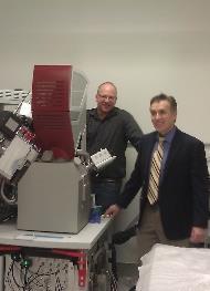
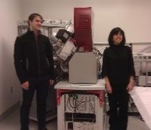
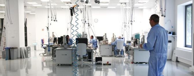
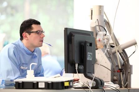
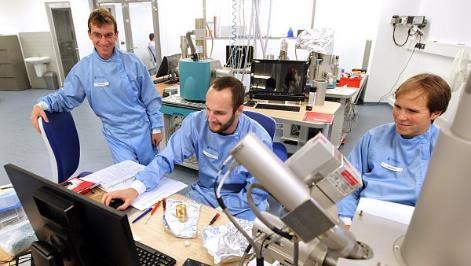
5 to UMD Nanocenter AIM Lab 2/19/ th Annual FIB-SEM Workshop, John Hopkins APL, Laurel MD 5

 Model: JEOL 2100 LaB 6 TEM Electron Gun: LaB6 Accelerating")
 EDS (Oxford) Electron Diffraction: SAD, NBD, CBED")

 Detectors: SEM and BSE; EDS (Bruker) Model: JEOL 2100")
/0.")
 EELS and Energy Filter TEM (EFTEM, Gatan) In-situ")
, 1.")

 Office Image Scanner Vacuum")

 EDS, CL, 5-GIS, Peltier stage,")
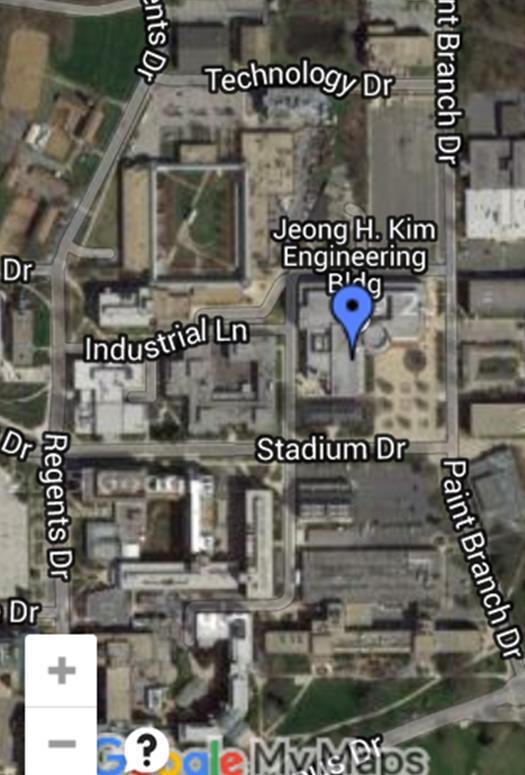
6 AIM LAB INSTRUMENTATION At Suite 1237, Jeong H. Kim Building High Resolution Analytical TEM Ultra High Resolution Analytical SEM Ultra High Resolution TEM/STEM Gallium FIB/SEM (GAIA) Model: JEOL 2100 LaB 6 TEM Electron Gun: LaB6 Accelerating Voltage: 100 to 200 kv Resolution: 0.23 nm (P-P)/0.14 nm (L) EDS (Oxford) Electron Diffraction: SAD, NBD, CBED Cameras: CCD and TV Cameras In-situ Experiments Model: Hitachi SU-70 UHR FEG-SEM Electron Gun: Schottky Field Emission Accelerating Voltage: 0.5 to 30 kv Resolution: 1.0 nm (15 kv), 1.6 nm (1 kv) Detectors: SEM and BSE; EDS (Bruker) Model: JEOL 2100 FEG-TEM Electron Gun: Schottky Field Emission Accelerating Voltage: 100 to 200 kv Resolution: nm (P-P)/0.14 nm (L) Electron Diffraction: SAD, NBD, CBED Cameras: two CCDs EDS (Oxford) EELS and Energy Filter TEM (EFTEM, Gatan) In-situ Experiments Electron Gun: Schottky Field Emission Accelerating Voltage: 0.2 ~ 30 kv Resolution: 1.0 nm (15 kv), 1.8 nm (1 kv) Ion Gun: Ga Liquid Metal Ion Source Accelerating Voltage: 0.5 ~ 30 kv Resolution: < 2.5 nm (30 kv) STEM, EDS, EBSD, TOF-SIMS, OP-200, 5-GIS, Peltier Stage, Low-Vac Xenon FIB/SEM (XEIA) Office Image Scanner Vacuum Evaporator Plasma Cleaner Optical Microscope Ion Mill Carbon Evaporator Electron Gun: Schottky Field Emission Accelerating Voltage: 0.2 ~ 30 kv Resolution: 1.0 nm (15 kv), 1.6 nm (1 kv) Ion Gun: Xe Plasma Ion Source Accelerating Voltage: 3 ~ 30 kv Resolution: 25 nm (30 kv) EDS, CL, 5-GIS, Peltier stage, Low-Vac Fume Hood Laminar Flow Hood 2/19/ th Annual FIB-SEM Workshop, John Hopkins APL, Laurel MD 8


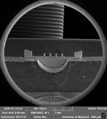
7 GAIA-3 FIB/SEM SFE, LMIS, Se -, R-BSe -, IB-Se -, IB-BSe - SI +, STEM, 2xEDS, EBSD, TOF-SIMS, 5-GIS, OP-200, STEM EDS F on Li EDS O on Li 2/19/ th Annual FIB-SEM Workshop, John Hopkins APL, Laurel MD 7


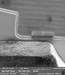
8 FIB-STEM Holder STEM-EDS in SEM (SOFC) STEM Position Rapid grid change for: STEM DF/BF, HR Se - STEM-EDS with EDS-1 2/19/ th Annual FIB-SEM Workshop, John Hopkins APL, Laurel MD 8

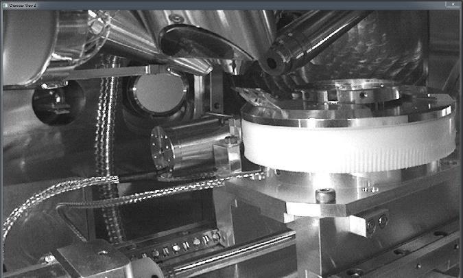
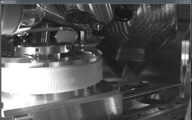
9 FIB-STEM Holder Additional Positions FIB-ORTHO: Cutout, TOF-SIMS FIB: Thinning, EDS-2 SEM: Lamella Attachment FIB FIB FIB FIB SEM FIB SEM SEM SEM 2/19/ th Annual FIB-SEM Workshop, John Hopkins APL, Laurel MD 9
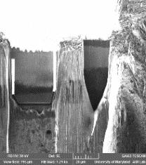
10 FIB-STEM Holder STEM imaging on round and lift-out grids In addition to STEM imaging, the FIB-STEM holder could be positioned for:» SEM attaching lamella to grid» FIB thinning lamella, EDS with enhanced count» FIB-ORTHO TOF-SIMS, lamella cut-out Change between any positions in under ~40 Sec 2/19/ th Annual FIB-SEM Workshop, John Hopkins APL, Laurel MD 10


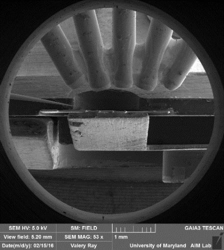
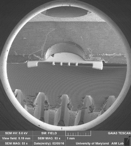
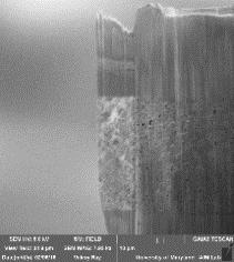
11 EDS on Porous Ceramic Lamella Improved spatial resolution on thinned area, prior to final thinning to TEM transparency FIB SEM FIB Orientation EDS: Main Element EDS: Inclusion 2/19/ th Annual FIB-SEM Workshop, John Hopkins APL, Laurel MD 11


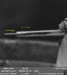
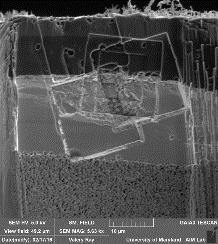
12 FIB / TOF-SIMS on Thick Lamella TOF SEM EDS: Sr Differences in Sr distribution visible in FIB/SIMS No differences in Sr distribution detected by EDS 2/19/ th Annual FIB-SEM Workshop, John Hopkins APL, Laurel MD 12
13 Summary Developed and demonstrated full-cycle TEM sample preparation process using Tescan FIB-STEM holder Utilized increased X-Ray counts in FIB position for highresolution EDS mapping on thinned lamella Utilized higher efficiency of secondary ion collection in FIB-ORTHO position for detecting variation in Strontium distribution near ceramic boundary by in-situ TOF-SIMS 2/19/ th Annual FIB-SEM Workshop, John Hopkins APL, Laurel MD 13
14 Acknowledgements Support of University of Maryland NanoCenter and its AIM Lab Image of STEM-EDS of Solid Electrolyte Fuel Cell provided by Joshua Taillon Instrumentation slide provided by Director of AIM Lab, Dr. Wen-An Chiou Challenging sample for FIB/SIMS & EDS provided by Wachsman s ceramic anode development team: Prof. Eric D. Wachsman Dr. Mohammed Hussain Abdul Jabbar Ke-Ji Pan 2/19/ th Annual FIB-SEM Workshop, John Hopkins APL, Laurel MD 14
15 9 th Annual FIB-SEM Workshop, John Hopkins APL, Laurel MD
EPIC: Keck-II: SPID:
 The Northwestern University Atomic and Nanoscale Characterization Experimental Center (NUANCE) was established during 2001-02 to integrate complementary analytical instruments and characterization capabilities
The New TEM facility at LCI, KSU. Min Gao Liquid Crystal Institute Kent State University
 The New TEM facility at LCI, KSU Min Gao Liquid Crystal Institute Kent State University 1 Questions to be answered How does TEM work? Why thin specimen? How to prepare one? What is the TEM at LCI like?
(Advanced) FIB sample preparation for (high performance) TEM analysis
 FIB sample preparation for (high performance) TEM analysis") (Advanced) FIB sample preparation for (high performance) TEM analysis Bertrand Van de Moortèle Laboratoire de Géologie de Lyon Terre, Planètes, Environnement ENS de Lyon CROSSBEAM MICROSCOPY Metz, June
(Advanced) FIB sample preparation for (high performance) TEM analysis Bertrand Van de Moortèle Laboratoire de Géologie de Lyon Terre, Planètes, Environnement ENS de Lyon CROSSBEAM MICROSCOPY Metz, June
Nova 600 NanoLab Dual beam Focused Ion Beam IITKanpur
 Nova 600 NanoLab Dual beam Focused Ion Beam system @ IITKanpur Dual Beam Nova 600 Nano Lab From FEI company (Dual Beam = SEM + FIB) SEM: The Electron Beam for SEM Field Emission Electron Gun Energy : 500
TESCAN S New generation of FIB-SEM microscope
 TESCAN S New generation of FIB-SEM microscope rising standards in sample preparation Key Features SEM COLUMN Versatile system for unlimited applications: resolution imaging (0.9 nm at 15 kev, 1.4 nm at
MSE 321 Structural Characterization
 Optical Microscope Plan Lenses In an "ideal" single-element lens system all planar wave fronts are focused to a point at distance f from the lens; therefore: Image near the optical axis will be in perfect
ELECTRON MICROSCOPE UNIT
 ELECTRON MICROSCOPE Director: Prof Richard Tilley Associate Director: Dr Nicholas Ariotti Lab Manager: Ms Katie Levick Administrative Assistant: Mr Michael Zhi UNIT Basement Level: F10 Chemical Sciences
Nanoscale voxel spectroscopy by simultaneous EELS and EDS tomography
 Electronic Supplementary Material (ESI) for Nanoscale. This journal is The Royal Society of Chemistry 2014 Supplementary Information Nanoscale voxel spectroscopy by simultaneous EELS and EDS tomography
Electron Microprobe Analysis 1 Nilanjan Chatterjee, Ph.D. Principal Research Scientist
 12.141 Electron Microprobe Analysis 1 Nilanjan Chatterjee, Ph.D. Principal Research Scientist Massachusetts Institute of Technology Electron Microprobe Facility Department of Earth, Atmospheric and Planetary
Electron Microprobe Analysis 1 Nilanjan Chatterjee, Ph.D. Principal Research Scientist
 12.141 Electron Microprobe Analysis 1 Nilanjan Chatterjee, Ph.D. Principal Research Scientist Massachusetts Institute of Technology Electron Microprobe Facility Department of Earth, Atmospheric and Planetary
Model : JEOL JSM 7610f
 Name Field Emission Electron Scanning Microscopy (FESEM) Make: JEOL India Pvt Ltd. Model : JEOL JSM 7610f Specification Electron gun : Schottky type field emission (T-FE) gun Electron Beam resolution (secondary
FIB Etching and Deposition on Nanoscale Studied by TEM and Numerical Modeling
 FIB Etching and Deposition on Nanoscale Studied by TEM and Numerical Modeling V. Ray, E. Chang, Sz.C. Liou, K. Toula, and W.A. Chiou vray@umd.edu 8 th FIB/SEM Workshop, John Hopkins APL, Laurel MD Outline
Electronic Supplementary Information (ESI)
") Electronic Supplementary Information (ESI) A thin-layered chromatography plate prepared from naphthalimide-based receptor immobilized SiO 2 nanoparticles as a portable chemosensor and adsorbent for Pb
Electronic Supplementary Information (ESI) A thin-layered chromatography plate prepared from naphthalimide-based receptor immobilized SiO 2 nanoparticles as a portable chemosensor and adsorbent for Pb
2012/01/20. Thierry EPICIER. MATEIS-CLYM, umr CNRS5510, Director METSA (FR 3507 CNRS) M. AOUINE, JP MILLET et al.
 M. AOUINE, JP MILLET et al.") 2012/01/20 Thierry EPICIER MATEIS-CLYM, umr CNRS5510, Director METSA (FR 3507 CNRS) thierry.epicier@insa-lyon.fr M. AOUINE, JP MILLET et al. MATERIALS SCIENCES & NANOTECHNOLOGIES HIGH RESOLUTION MICROSCOPY
2012/01/20 Thierry EPICIER MATEIS-CLYM, umr CNRS5510, Director METSA (FR 3507 CNRS) thierry.epicier@insa-lyon.fr M. AOUINE, JP MILLET et al. MATERIALS SCIENCES & NANOTECHNOLOGIES HIGH RESOLUTION MICROSCOPY
HOW TO APPROACH SCANNING ELECTRON MICROSCOPY AND ENERGY DISPERSIVE SPECTROSCOPY ANALYSIS. SCSAM Short Course Amir Avishai
 HOW TO APPROACH SCANNING ELECTRON MICROSCOPY AND ENERGY DISPERSIVE SPECTROSCOPY ANALYSIS SCSAM Short Course Amir Avishai RESEARCH QUESTIONS Sea Shell Cast Iron EDS+SE Fe Cr C Objective Ability to ask the
Everhart-Thornley detector
 SEI Detector Everhart-Thornley detector Microscope chamber wall Faraday cage Scintillator Electrons in Light pipe Photomultiplier Electrical signal out Screen Quartz window +200 V +10 kv Always contains
User Fees for the 4D LABS Characterization Facility
 User Fees for the 4D LABS Characterization Facility 1. Imaging Fees Service SEM 1 - Helios: SEM/EDS mode SEM/EDS mode with FIB functions Cryo mode setup SEM 2 Nova NanoSEM SEM/EDS mode SEM/EDS mode with
PHYS-E0541:Special Course in Physics Gas phase synthesis of carbon nanotubes for thin film application. Electron Microscopy. for
 PHYS-E0541:Special Course in Physics Gas phase synthesis of carbon nanotubes for thin film application Electron Microscopy for Introduction to Electron Microscopy Carbon Nanomaterials (nanotubes) Dr. Hua
Pd-P nanoalloys supported on porous carbon frame as efficient catalyst for benzyl alcohol oxidation
 Electronic Supplementary Material (ESI) for Catalysis Science & Technology. This journal is The Royal Society of Chemistry 2018 Supporting information Pd-P nanoalloys supported on porous carbon frame as
The illumination source: the electron beam
 The SEM Column The illumination source: the electron beam The probe of the electron microscope is an electron beam with very high and stable energy (10-100 kev) in order to get images with high resolution.
CBE Science of Engineering Materials. Scanning Electron Microscopy (SEM)
") CBE 30361 Science of Engineering Materials Scanning Electron Microscopy (SEM) Scale of Structure Organization Units: micrometer = 10-6 m = 1µm nanometer= 10-9 m = 1nm Angstrom = 10-10 m = 1Å A hair is
CBE 30361 Science of Engineering Materials Scanning Electron Microscopy (SEM) Scale of Structure Organization Units: micrometer = 10-6 m = 1µm nanometer= 10-9 m = 1nm Angstrom = 10-10 m = 1Å A hair is
Low Vacuum Scanning Electron Microscopy and Microanalysis
 Low Vacuum Scanning Electron Microscopy and Microanalysis Principles and Practice of Variable Pressure/Environmental Scanning Electron Microscopy (VP-ESEM), Debbie J Stokes, John Wiley&Sons 2008 Several
An environment designed for success
 An environment designed for success The nanofab is a centralized, open-access, training, service, and collaboration facility, focused on academic research and industrial applications in micro- and nanoscale
Gaetano L Episcopo. Scanning Electron Microscopy Focus Ion Beam and. Pulsed Plasma Deposition
 Gaetano L Episcopo Scanning Electron Microscopy Focus Ion Beam and Pulsed Plasma Deposition Hystorical background Scientific discoveries 1897: J. Thomson discovers the electron. 1924: L. de Broglie propose
Chapter 9. Electron mean free path Microscopy principles of SEM, TEM, LEEM
 Chapter 9 Electron mean free path Microscopy principles of SEM, TEM, LEEM 9.1 Electron Mean Free Path 9. Scanning Electron Microscopy (SEM) -SEM design; Secondary electron imaging; Backscattered electron
= 6 (1/ nm) So what is probability of finding electron tunneled into a barrier 3 ev high?
 So what is probability of finding electron tunneled into a barrier 3 ev high?") STM STM With a scanning tunneling microscope, images of surfaces with atomic resolution can be readily obtained. An STM uses quantum tunneling of electrons to map the density of electrons on the surface
STM STM With a scanning tunneling microscope, images of surfaces with atomic resolution can be readily obtained. An STM uses quantum tunneling of electrons to map the density of electrons on the surface
SUPPORTING INFORMATION
 Electronic Supplementary Material (ESI) for Chemical Communications. This journal is The Royal Society of Chemistry 2017 SUPPORTING INFORMATION Synthesis of Circular and Triangular Gold Nanorings with
Characterisation of Catalysts Using Secondary and Backscattered Electron In-lens Detectors
 Platinum Metals Rev., 2014, 58, (2), 106 110 FINAL ANALYSIS Characterisation of Catalysts Using Secondary and Backscattered Electron In-lens Detectors Heterogeneous catalysis often involves the use of
Dual Beam Helios Nanolab 600 and 650
 Dual Beam Helios Nanolab 600 and 650 In the Clean Room facilities of the INA LMA, several lithography facilities permit to pattern structures at the micro and nano meter scale and to create devices. In
How to Use the Devices in the Analytical Instrument Laboratory
 How to Use the Devices in the Analytical Instrument Laboratory 1. Eligible users To be eligible, the user must be a member of the faculty or staff, a researcher, or a Waseda University student. If the
Transmission Electron Microscopy. Part #2 High Resolution Imaging XEDS EELS spectroscopies Aberration corrected TEM
 Transmission Electron Microscopy Part #2 High Resolution Imaging XEDS EELS spectroscopies Aberration corrected TEM Nicolas Menguy Institut de Minéralogie, de Physique des Matériaux et de Cosmochimie Part
h p λ = mν Back to de Broglie and the electron as a wave you will learn more about this Equation in CHEM* 2060
 Back to de Broglie and the electron as a wave λ = mν h = h p you will learn more about this Equation in CHEM* 2060 We will soon see that the energies (speed for now if you like) of the electrons in the
Imaging Carbon materials with correlative Raman-SEM microscopy. Introduction. Raman, SEM and FIB within one chamber. Diamond.
 Imaging Carbon materials with correlative Raman-SEM microscopy Application Example Carbon materials are widely used in many industries for their exceptional properties. Electric conductance, light weight,
Massachusetts Institute of Technology. Dr. Nilanjan Chatterjee
 Massachusetts Institute of Technology Dr. Nilanjan Chatterjee Electron Probe Micro-Analysis (EPMA) Imaging and micrometer-scale chemical compositional analysis of solids Signals produced in The Electron
*Specifications subject to change without notice.
 The Power of STEM *Specifications subject to change without notice. No. 1301G040C 1101E010C Printed in Japan, Kp Atomic Resolution Analytical Microscope Serving Advanced Technology Atomic Resolution Analytical
Energy-Filtering. Transmission. Electron Microscopy
 Part 3 Energy-Filtering Transmission Electron Microscopy 92 Energy-Filtering TEM Principle of EFTEM expose specimen to mono-energetic electron radiation inelastic scattering in the specimen poly-energetic
Chapter 2 Instrumentation for Analytical Electron Microscopy Lecture 5. Chapter 2 CHEM 793, 2011 Fall 1
 Chater Instrumentation for Analytical Electron Microscoy Lecture 5 Chater CHEM 793, 011 Fall 1 Outline Electron Sources (Electron Guns) Thermionic: LaB 6 or W Field emission gun: cold or Schottky Lenses
Supporting Information
 Supporting Information Toward an Ideal Polymer Binder Design for High-Capacity Battery Anodes Mingyan Wu, 1 Xingcheng Xiao, 2 Nenad Vukmirovic, 3 Shidi Xun, 1 Prodip K. Das, 1 Xiangyun Song, 1 Paul Olalde-Velasco,
EDS on the Nanoscale in TEM/STEM and SEM
 EDS on the Nanoscale in TEM/STEM and SEM Bruker Nano Analytics, Berlin, Germany Webinar, June 14, 2017 Innovation with Integrity Presenters Dr. Meiken Falke Global Product Manager TEM Bruker Nano Analytics,
Conventional Transmission Electron Microscopy. Introduction. Text Books. Text Books. EMSE-509 CWRU Frank Ernst
 Text Books Conventional Transmission Electron Microscopy EMSE-509 CWRU Frank Ernst D. B. Williams and C. B. Carter: Transmission Electron Microscopy, New York: Plenum Press (1996). L. Reimer: Transmission
Scanning Electron Microscopy
 Scanning Electron Microscopy Field emitting tip Grid 2kV 100kV Anode ZEISS SUPRA Variable Pressure FESEM Dr Heath Bagshaw CMA bagshawh@tcd.ie Why use an SEM? Fig 1. Examples of features resolvable using
IMAGING DIFFRACTION SPECTROSCOPY
 TEM Techniques TEM/STEM IMAGING DIFFRACTION SPECTROSCOPY Amplitude contrast (diffracion contrast) Phase contrast (highresolution imaging) Selected area diffraction Energy dispersive X-ray spectroscopy
Two-dimensional homologous perovskites as light absorbing materials for solar cell applications
 Supporting Information for Two-dimensional homologous perovskites as light absorbing materials for solar cell applications Duyen H. Cao, Constantinos C. Stoumpos, Omar K. Farha,, Joseph T. Hupp, and Mercouri
object objective lens eyepiece lens
 Advancing Physics G495 June 2015 SET #1 ANSWERS Field and Particle Pictures Seeing with electrons The compound optical microscope Q1. Before attempting this question it may be helpful to review ray diagram
raw materials C V Mn Mg S Al Ca Ti Cr Si G H Nb Na Zn Ni K Co A B C D E F
 Today s advanced batteries require a range of specialized analytical tools to better understand the electrochemical processes that occur during battery cycling. Evans Analytical Group (EAG) offers a wide-range
Atomic Force/Magnetic Force Microscope
 Atomic Force/Magnetic Force Microscope Veeco Instruments Dimension 3000 SPM with Nanoscope IIIa controller Atomic Force Microscopy Mode Magnetic Force Microscopy Mode Vibration isolation and sound proof
Chapter 10. Nanometrology. Oxford University Press All rights reserved.
 Chapter 10 Nanometrology Oxford University Press 2013. All rights reserved. 1 Introduction Nanometrology is the science of measurement at the nanoscale level. Figure illustrates where nanoscale stands
Preamble: Emphasis: Material = Device? MTSE 719 PHYSICAL PRINCIPLES OF CHARACTERIZATION OF SOLIDS
 MTSE 719 PHYSICAL PRINCIPLES OF CHARACTERIZATION OF SOLIDS MTSE 719 - PHYSCL PRIN CHARACTIZTN SOLIDS Section # Call # Days / Times 001 96175 -View Book Info - F:100PM - 355PM - TIER114 Preamble: Core course
CHARACTERIZATION of NANOMATERIALS KHP
 CHARACTERIZATION of NANOMATERIALS Overview of the most common nanocharacterization techniques MAIN CHARACTERIZATION TECHNIQUES: 1.Transmission Electron Microscope (TEM) 2. Scanning Electron Microscope
Scanning Electron Microscopy
 Scanning Electron Microscopy Amanpreet Kaur 1 www.reading.ac.uk/emlab Scanning Electron Microscopy What is scanning electron microscopy? Basic features of conventional SEM Limitations of conventional SEM
Electronic Supplementary Information. Low-temperature Benchtop-synthesis of All-inorganic Perovskite Nanowires
 Electronic Supplementary Material (ESI) for Nanoscale. This journal is The Royal Society of Chemistry 2017 Electronic Supplementary Information Low-temperature Benchtop-synthesis of All-inorganic Perovskite
3D Boron doped Carbon Nanorods/Carbon-Microfiber Hybrid Composites: Synthesis and Applications as Highly Stable Proton Exchange Membrane Fuel Cell
 Electronic Supplementary Information for Journal of Materials Chemistry 3D Boron doped Carbon Nanorods/Carbon-Microfiber Hybrid Composites: Synthesis and Applications as Highly Stable Proton Exchange Membrane
ECE Semiconductor Device and Material Characterization
 ECE 4813 Semiconductor Device and Material Characterization Dr. Alan Doolittle School of Electrical and Computer Engineering Georgia Institute of Technology As with all of these lecture slides, I am indebted
FIB - SIMS. Focussed Ion Beam Secondary Ion Mass Spectrometry.
 FIB - SIMS Focussed Ion Beam Secondary Ion Mass Spectrometry Outline Introduction to Hiden Analytical Introduction to SIMS FIB-SIMS - Introduction and key features FIB-SIMS - Applications data Hiden SIMS
MT Electron microscopy Scanning electron microscopy and electron probe microanalysis
 MT-0.6026 Electron microscopy Scanning electron microscopy and electron probe microanalysis Eero Haimi Research Manager Outline 1. Introduction Basics of scanning electron microscopy (SEM) and electron
WorkShop Audace. INSA ROUEN 8 juin 2012
 WorkShop Audace INSA ROUEN 8 juin 2012 Groupe de Physique des Matériaux Failure analysis of the HEMT GaN Cécile Genevois 8 juin 2012 AGENDA Context GPM presentation GPM: High Technology instruments Power
Transmutation Reaction Induced by Deuterium Permeation Through Nanostructured Multi-layer Thin Film
 106 Transmutation Reaction Induced by Deuterium Permeation Through Nanostructured Multi-layer Thin Film SHIGENORI TSURUGA *1 KENJI MUTA *1 YUTAKA TANAKA *2 TADASHI SHIMAZU *3 KOJI FUJIMORI *4 TAKEHIKO
Why microscopy?
 Electron Microscopy Why microscopy? http://www.cellsalive.com/howbig.htm 2 Microscopes are used as magnifying tools (although not exclusively as will see later on). The resolution of the human eye is limited
From Nanoparticles to Single Atoms, EDS of Electron Transparent Samples. M. Falke, et al.
 From Nanoparticles to Single Atoms, EDS of Electron Transparent Samples M. Falke, et al. 1 Presenters Dr. Meiken Falke Product Manager EDS/TEM, Bruker Nano Analytics, Berlin, Germany Dr. Igor Nemeth Application
Supplementary Information
 Electronic Supplementary Material (ESI) for Physical Chemistry Chemical Physics. This journal is the Owner Societies 2015 Supplementary Information Vertical Heterostructures of MoS2 and Graphene Nanoribbons
HIGH-TEMPERATURE CADMIUM-FREE NANOPHOSPHORS FOR DAYLIGHT-QUALITY WHITE LEDS
 CPS S1 / R1 Intensity (CPS) HIGH-TEMPERATURE CADMIUM-FREE NANOPHOSPHORS FOR DAYLIGHT-QUALITY WHITE LEDS REU Student: Nathaniel C. Cook Graduate Student Mentor: Brian A. Akins Faculty Mentor: Dr. Marek
Synthesis of Colloidal Au-Cu 2 S Heterodimers via Chemically Triggered Phase Segregation of AuCu Nanoparticles
 SUPPORTING INFORMATION Synthesis of Colloidal Au-Cu 2 S Heterodimers via Chemically Triggered Phase Segregation of AuCu Nanoparticles Nathan E. Motl, James F. Bondi, and Raymond E. Schaak* Department of
April 10th-12th, 2017
 Thomas LaGrange, Ph.D. Faculty Lecturer and Senior Staff Scientist Introduction: Basics of Transmission Electron Microscopy (TEM) TEM Doctoral Course MS-637 April 10th-12th, 2017 Outline 1. What is microcopy?
Nanoporous metals by dealloying multicomponent metallic glasses. Chen * Institute for Materials Research, Tohoku University, Sendai , Japan
 Supporting information for: Nanoporous metals by dealloying multicomponent metallic glasses Jinshan Yu, Yi Ding, Caixia Xu, Akihisa Inoue, Toshio Sakurai and Mingwei Chen * Institute for Materials Research,
MSE 321 Structural Characterization
 Auger Spectroscopy Auger Electron Spectroscopy (AES) Scanning Auger Microscopy (SAM) Incident Electron Ejected Electron Auger Electron Initial State Intermediate State Final State Physical Electronics
Final exam: take-home part
 Final exam: take-home part! List five things that can be done to improve this class. Be specific; give much detail.! (You will be penalized only for insulting comments made for no benefit; you will not
Scanning Electron Microscopy (SEM) with Energy Dispersive Spectroscopy (EDS) Analysis The samples were also characterized by scanning electron
 with Energy Dispersive Spectroscopy (EDS) Analysis The samples were also characterized by scanning electron") Electronic Supplementary Material (ESI) for RSC Advances. This journal is The Royal Society of Chemistry 2016 Scanning Electron Microscopy (SEM) with Energy Dispersive Spectroscopy (EDS) Analysis The samples
Electronic Supplementary Material (ESI) for RSC Advances. This journal is The Royal Society of Chemistry 2016 Scanning Electron Microscopy (SEM) with Energy Dispersive Spectroscopy (EDS) Analysis The samples
Rapid, Efficient Phase Pure Synthesis of Ca 2 AlNO 3 Layered Double Hydroxide
 Electronic Supplementary Material (ESI) for Journal of Materials Chemistry A. This journal is The Royal Society of Chemistry 2015 Supporting Information Rapid, Efficient Phase Pure Synthesis of Ca 2 AlNO
Resolving Questions of Biological Interface Chemistry with TOF-SIMS and FIB-TOF Tomography
 Resolving Questions of Biological Interface Chemistry with TOF-SIMS and FIB-TOF Tomography Gregory L. Fisher, John S. Hammond & Scott R. Bryan, Physical Electronics With acknowledgements to: Prof. Reinhard
CURRICULUM VITAE. Department of Physics (D.P), College of Science (C.S), Sudan University of Science and
, College of Science (C.S), Sudan University of Science and") CURRICULUM VITAE DATE: July 2016 PERSONAL DATA: NAME: Abd Ellateef Abbass Abd Ellateef Mohammed Khair (AE. Abbass) NATIONALITY: Sudanese GENDER: Male PLACE AND DATE OF BIRTH: Sudan, 02 / May / 1977 LANGUAGES:
CURRICULUM VITAE DATE: July 2016 PERSONAL DATA: NAME: Abd Ellateef Abbass Abd Ellateef Mohammed Khair (AE. Abbass) NATIONALITY: Sudanese GENDER: Male PLACE AND DATE OF BIRTH: Sudan, 02 / May / 1977 LANGUAGES:
Microscopy: Principles
 Low Voltage Electron Microscopy: Principles and Applications Edited by David C. Bell Harvard University, USA and Natasha Erdman JEOL USA Inc., USA Published in association with the Royal Microscopical
Lecture 22 Ion Beam Techniques
 Lecture 22 Ion Beam Techniques Schroder: Chapter 11.3 1/44 Announcements Homework 6/6: Will be online on later today. Due Wednesday June 6th at 10:00am. I will return it at the final exam (14 th June).
GSA Data Repository Item Wacey et al.
 GSA Data Repository Item 2015025 Wacey et al. Figure DR1. Occurrence of putative framboidal pyrite from the late Ediacaran of the Catalina Dome, Bonavista Peninsula, Newfoundland (sample WM1, c. 560 Ma
Chemical Analysis in TEM: XEDS, EELS and EFTEM. HRTEM PhD course Lecture 5
 Chemical Analysis in TEM: XEDS, EELS and EFTEM HRTEM PhD course Lecture 5 1 Part IV Subject Chapter Prio x-ray spectrometry 32 1 Spectra and mapping 33 2 Qualitative XEDS 34 1 Quantitative XEDS 35.1-35.4
Two-Dimensional (C 4 H 9 NH 3 ) 2 PbBr 4 Perovskite Crystals for. High-Performance Photodetector. Supporting Information for
 2 PbBr 4 Perovskite Crystals for. High-Performance Photodetector. Supporting Information for") Supporting Information for Two-Dimensional (C 4 H 9 NH 3 ) 2 PbBr 4 Perovskite Crystals for High-Performance Photodetector Zhenjun Tan,,ǁ, Yue Wu,ǁ, Hao Hong, Jianbo Yin, Jincan Zhang,, Li Lin, Mingzhan
Supporting Information for Two-Dimensional (C 4 H 9 NH 3 ) 2 PbBr 4 Perovskite Crystals for High-Performance Photodetector Zhenjun Tan,,ǁ, Yue Wu,ǁ, Hao Hong, Jianbo Yin, Jincan Zhang,, Li Lin, Mingzhan
Determination of Minimum Detectable Partial Pressure (MDPP) of QMS and its Uncertainty
 of QMS and its Uncertainty") Workshop on Towards more reliable partial and outgassing rate measurements Berlin, Germany, January 30 - February 1, 2017 Determination of Minimum Detectable Partial Pressure (MDPP) of QMS and its Uncertainty
Workshop on Towards more reliable partial and outgassing rate measurements Berlin, Germany, January 30 - February 1, 2017 Determination of Minimum Detectable Partial Pressure (MDPP) of QMS and its Uncertainty
Supporting Information for: Emulsion-assisted synthesis of monodisperse binary metal nanoparticles
 Supporting Information for: Emulsion-assisted synthesis of monodisperse binary metal nanoparticles Zhen Yin, Ding Ma* and Xinhe Bao* Synthesis of the PdCu nanoparticles: All synthesis was carried out under
Auger Electron Spectroscopy Overview
 Auger Electron Spectroscopy Overview Also known as: AES, Auger, SAM 1 Auger Electron Spectroscopy E KLL = E K - E L - E L AES Spectra of Cu EdN(E)/dE Auger Electron E N(E) x 5 E KLL Cu MNN Cu LMM E f E
Applications of XPS, AES, and TOF-SIMS
 Applications of XPS, AES, and TOF-SIMS Scott R. Bryan Physical Electronics 1 Materials Characterization Techniques Microscopy Optical Microscope SEM TEM STM SPM AFM Spectroscopy Energy Dispersive X-ray
Gold nanothorns macroporous silicon hybrid structure: a simple and ultrasensitive platform for SERS
 Supporting Information Gold nanothorns macroporous silicon hybrid structure: a simple and ultrasensitive platform for SERS Kamran Khajehpour,* a Tim Williams, b,c Laure Bourgeois b,d and Sam Adeloju a
ABNORMAL X-RAY EMISSION FROM INSULATORS BOMBARDED WITH LOW ENERGY IONS
 302 ABNORMAL X-RAY EMISSION FROM INSULATORS BOMBARDED WITH LOW ENERGY IONS M. Song 1, K. Mitsuishi 1, M. Takeguchi 1, K. Furuya 1, R. C. Birtcher 2 1 High Voltage Electron Microscopy Station, National
SCANNING THERMAL MICROSCOPY OF THERMOELECTRIC PULSED LASER DEPOSITED NANOSTRUCTURES
 SCANNING THERMAL MICROSCOPY OF THERMOELECTRIC PULSED LASER DEPOSITED NANOSTRUCTURES VANIŠ Jan 1,2, ZELINKA Jiří 1, ZEIPL Radek 1, JELÍNEK Miroslav 1, KOCOUREK Tomáš 1, REMSA Jan 1, NAVRÁTIL Jiří 3 1 Institute
MSE 321 Structural Characterization
 Auger Spectroscopy Auger Electron Spectroscopy (AES) Scanning Auger Microscopy (SAM) Incident Electron Ejected Electron Auger Electron Initial State Intermediate State Final State Physical Electronics
Electron probe microanalysis - Electron microprobe analysis EPMA (EMPA) What s EPMA all about? What can you learn?
 What s EPMA all about? What can you learn?") Electron probe microanalysis - Electron microprobe analysis EPMA (EMPA) What s EPMA all about? What can you learn? EPMA - what is it? Precise and accurate quantitative chemical analyses of micron-size
Electron probe microanalysis - Electron microprobe analysis EPMA (EMPA) What s EPMA all about? What can you learn? EPMA - what is it? Precise and accurate quantitative chemical analyses of micron-size
Analytical Methods for Materials
 Analytical Methods for Materials Lesson 21 Electron Microscopy and X-ray Spectroscopy Suggested Reading Leng, Chapter 3, pp. 83-126; Chapter 4, pp. 127-160; Chapter 6, pp. 191-219 P.J. Goodhew, J. Humphreys
Supporting Information
 Supporting Information Universal, In-Situ Transformation of Bulky Compounds into Nanoscale Catalysts by High Temperature Pulse Shaomao Xu 1, (a), Yanan Chen 1, (a), Yiju Li 1, (a), Aijiang Lu 1, Yonggang
Supporting Information
 Supporting Information Pt Nanoparticles Anchored Molecular Self-Assemblies of DNA: An Extremely Stable and Efficient HER Electrocatalyst with Ultra-Low Pt Content Sengeni Anantharaj, $ Pitchiah E. Karthik,
Introduction to Microscopy. Boonrat Lohwongwatana
 Introduction to Microscopy Boonrat Lohwongwatana boonrat@gmail.com http://ows.public.sembach.af.mil/index.cfm Avoiding stereological bias inherent to the appearance of 3-D objects on
NUANCE Center. Northwestern University Atomic and Nanoscale Experimental Characterization Center. Professor Vinayak P. Dravid, Ph.D.
 NUANCE Center Northwestern University Atomic and Nanoscale Experimental Characterization Center Professor Vinayak P. Dravid, Ph.D. Director NUANCE CENTER NU Atomic and Nanoscale Characterization Experimental
Ionization Techniques Part IV
 Ionization Techniques Part IV CU- Boulder CHEM 5181 Mass Spectrometry & Chromatography Presented by Prof. Jose L. Jimenez High Vacuum MS Interpretation Lectures Sample Inlet Ion Source Mass Analyzer Detector
Interactions with Matter
 Manetic Lenses Manetic fields can displace electrons Manetic field can be produced by passin an electrical current throuh coils of wire Manetic field strenth can be increased by usin a soft ferromanetic
Role of Re and Ru in Re Ru/C Bimetallic Catalysts for the
 Role of Re and Ru in Re Ru/C Bimetallic Catalysts for the Aqueous Hydrogenation of Succinic Acid Xin Di a, Chuang Li a, Bingsen Zhang b, Ji Qi a, Wenzhen Li c, Dangsheng Su b, Changhai Liang a, * a Laboratory
Scanning Electron Microscopy & Ancillary Techniques
 Scanning Electron Microscopy & Ancillary Techniques By Pablo G. Caceres-Valencia The prototype of the first Stereoscan supplied by the Cambridge Instrument Company to the dupont Company, U.S.A. (1965)
Body Centered Cubic Magnesium Niobium Hydride with Facile Room Temperature Absorption and Four Weight Percent Reversible Capacity
 Electronic Supplementary Information (ESI) for Energy & Environmental Science This journal is The Royal Society of Chemistry 212 Supporting Information Body Centered Cubic Magnesium Niobium Hydride with
FIELD EMISSION SCANNING ELECTRON MICROSCOPY
 FIELD EMISSION SCANNING ELECTRON MICROSCOPY Make: Carl Zeiss, Germany Model: SUPRA 55VP, Gemini Column. With air lock system Detectors; 1, Secondary Electron 1 (In Lens) 2, Secondary Electron 2(SE2) 3,
Supporting Information for
 Supporting Information for 2D/2D g-c 3 N 4 /MnO 2 nanocomposite as a direct Z-scheme photocatalyst for enhanced photocatalytic activity Pengfei Xia, Bicheng Zhu, Bei Cheng, Jiaguo Yu, *,, and Jingsan Xu
Supporting Information
 1 Supporting Information Photoluminescent Carbogenic Dots A. B. Bourlinos, A. Stassinopoulos, D. Anglos, R. Zboril, V. Georgakilas, E. P. Giannelis *, Institute of Materials Science, NCSR Demokritos, Ag.
Opportunities for Advanced Plasma and Materials Research in National Security
 Opportunities for Advanced Plasma and Materials Research in National Security Prof. J.P. Allain allain@purdue.edu School of Nuclear Engineering Purdue University Outline: Plasma and Materials Research
Ionic Liquid Ion Sources in the Processing of Materials and Other Applications
 Ionic Liquid Ion Sources in the Processing of Materials and Other Applications Paulo Lozano Massachusetts Institute of Technology Materials and Processes Far From Equilibrium Workshop November 3, 2010
Novel fluorescent matrix embedded carbon quantum dots enrouting stable gold and silver hydrosols
 Novel fluorescent matrix embedded carbon quantum dots enrouting stable gold and silver hydrosols Shouvik Mitra a, Sourov Chandra b, Prasun Patra a, Panchanan Pramanik b *, Arunava Goswami a * a AERU, Biological