2D Materials Research Activities at the NEST lab in Pisa, Italy. Stefan Heun NEST, Istituto Nanoscienze-CNR and Scuola Normale Superiore, Pisa, Italy
|
|
|
- Benjamin Thompson
- 5 years ago
- Views:
Transcription
1 2D Materials Research Activities at the NEST lab in Pisa, Italy Stefan Heun NEST, Istituto Nanoscienze-CNR and Scuola Normale Superiore, Pisa, Italy
2 2D Materials Research Activities at the NEST lab in Pisa, Italy Stefan Heun NEST, Istituto Nanoscienze-CNR and Scuola Normale Superiore, Pisa, Italy
3 Outline CNR Nano NEST Pisa My Research Activities
4 Outline CNR Nano NEST Pisa My Research Activities

 project admin,")
5 Institute of Nanoscience Established on February 2010 Pisa: L. Sorba Lecce: D. Pisignano Modena: E. Molinari Adm. Genova (with Nano, SPIN, IOM) project admin, recruitment
6 Mission The primary objective of the Institute is the fundamental study and the manipulation of systems at the nanometric scale. Its wide and multidisciplinary research activities include: Synthesis and fabrication of nanostructures and devices. Experimental and theoretical-computational studies of their properties and functionality. Knowledge and expertise are used to develop applications in several fields, from energy and environment to nanomechanics, nano(bio)technologies, and nanomedicine. Special attention to projects and advanced technologies of industrial interest.

7 Institute of Nanoscience Interdisciplinary research activities where physicists, chemists and biologists do science at the nanoscale. Strong interaction between theory and experiments Strong interaction with the Universities (SNS, Unimore, Salento) 7
8 Equipment intensive Nanofabrication: bottom-up: growth (CBE, CVD) and chemical and bio synthesis top-down: clean rooms, EBL, FIB Microscopies : SEM, TEM, AFM, SNOM, STM, two photon microscopy, single molecule imaging, scanning gate microscopy Spectroscopies: Transport and optics at low T and H fields, electron spectroscopy, optical tweezers Theory: Cluster, dedicated agreement with CINECA 8

9 Personnel 2014 Total: % 31% Employees Associates Postdocs 48% Associates: mainly from University, including students (Master and PhD) 9

10 Publications Nano Istituto Nanoscienze is the Cnr institute with the highest number of publications in 2012 in the Nature Group journals according to the recently published Nature Publishing Index. 10
 REGIONAL NATIONAL EUROPEAN 2,000,000.00 1,000,000.00 0.")
11 Funding ,000, ,000, ,000, ,000, ,000, ,000, ,000, CNR-FFO INDUSTRY PON (SOUTH ITALY ONLY) REGIONAL NATIONAL EUROPEAN 2,000, ,000,

12 Scientific Council 12
13
14 Outline CNR Nano NEST Pisa My Research Activities

15 NEST Facilities - NEST Pisa


16 NEST Pisa National Enterprise for nanoscience and nanotechnology NEST is an interdisciplinary research and training centre where physicists, chemists and biologists investigate scientific issues at the nanoscale.
17 Research NEST Pisa NanoPhysics 1. Quantum transport and phase coherent effects in superconductors 2. Physics of low-dimensional semiconductor systems 3. Graphene (Flagship) Advanced Photonics 4. Intersubband polaritonics 5. Silicon-Germanium optoelectronics 6. THz photonics 7. OptoElectronics Materials: from nanoscale to bulk single crystals NanoBioScience 8. Visualizing brain function and structure in the living mouse 9. Lab-on-a-chip technologies 10. Nanoscale and single-molecule spectroscopy and imaging of soft matter

18 NEST Facilities - NEST Pisa

19 NEST Facilities - NEST Pisa
20 NEST

21 NEST 0.1 Low-temperature magneto transport and optics
22 0.2 Scanning Gate Microscopy NEST

23 NEST 0.3 CVD-based growth of graphene nanostructures

24 NEST 0.4 Transmission Electron Microscopy Lab

25 NEST 0.5 CBE, Plasma Etching and Deposition
")
26 Theory (DFT) NEST
27 0.6 Coherent Raman Spectroscopy NEST


28 NEST Micro-Raman 0.6 Coherent Raman Spectroscopy

29 0.7 Superconductivity NEST


30 NEST 0.9 UHV-VT-STM AFM 4K UHV-LT-STM Micro-Raman
31 NEST
32 1.1 Clean Room Facility NEST

33 NEST 1.1 Clean Room Facility SEM

34 NEST 1.1 Clean Room Facility AFM

35 NEST 1.5 Single-molecule Confocal Microscopy

36 NEST 1.6 THZ Quantum Cascade Lasers and DNSOM

37 NEST 1.12 Bio Chemistry and Molecular Biology

38 1.14 Lab-on-a-Chip Tecnologies NEST

39 1.15 In vivo Two-Photon Imaging NEST
40 Outline CNR Nano NEST Pisa My Research Activities

41 Yuya Murata Stefan Heun Stefano Guiducci Abhishek Kumar Luca Planat Stefano Roddaro Shaohua Xiang

 the manipulation of samples on")


42 Research Activities The physics of low-dimensional systems. This includes three aspects: (i) the synthesis of nanostructures, (ii) the manipulation of samples on the nanometer-scale, and (iii) their characterization with spatially resolved spectroscopic techniques. (i) synthesis of nanostructures (iii) Sample characterization with spatially resolved spectroscopic techniques (ii) manipulation of samples on the nanometer-scale

43 Surface Science & Magneto-Transport UHV-VT-STM & Scanning Gate Microscopy 300 mk, 9 T UHV-LT-STM

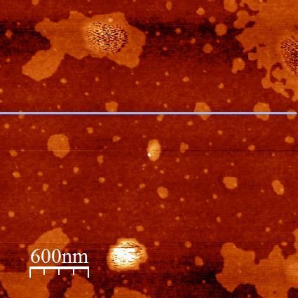
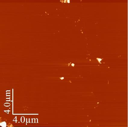
44 Projects Graphene for Hydrogen Storage Phosphorene G. Gervais, Mc Gill University, Montreal, Canada 2D Materials S. Suzuki, NTT High-mobility Graphene
45 Recent Activities SGM on QPCs in III-V 2DEGS Magneto-transport in Graphene Hydrogenated Graphene Hydrogen Storage in Graphene Phosphorene
46
 948.")
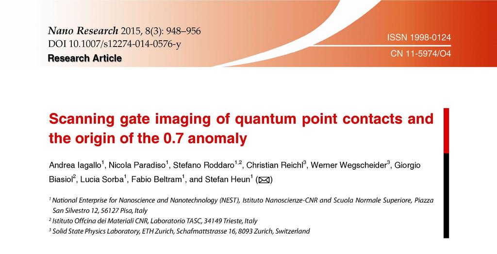
47 0.7 Anomaly A. Iagallo et al., Nano Research 8 (2015) 948.
48


49 Bilayer-induced asymmetric quantum Hall effect A. Iagallo et al., Semicond. Sci. Technol. 30 (2015)
50

51 Single-crystal CVD graphene V. Miseikis et al., 2D Mater. 2 (2015)
52
53 Berry Phase in Graphene K. Bennaceur et al., Phys. Rev. B, submitted.
54

 T.")
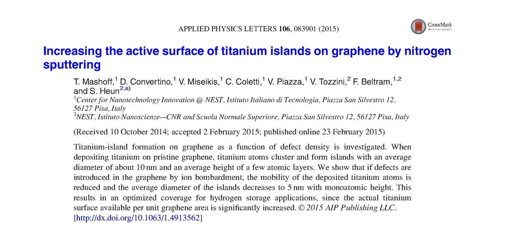
55 Number of islands Hydrogen storage in Ti-functionalized graphene Average Number of Islands per 100 nm Sputter Energy (ev) T. Mashoff et al., Appl. Phys. Lett. 106 (2015)
56
57 M. Serrano-Ruiz et al., in preparation. Phosphorene Flakes
Metal-functionalized Graphene for Hydrogen Storage
 Metal-functionalized Graphene for Hydrogen Storage Stefan Heun NEST, Istituto Nanoscienze-CNR and Scuola Normale Superiore Pisa, Italy NEST Pisa Research themes @ NEST Pisa National Enterprise for nanoscience
Semiconductor Nanowires. Stefan Heun NEST, Istituto Nanoscienze-CNR and Scuola Normale Superiore, Pisa, Italy
 Semiconductor Nanowires Stefan Heun NEST, Istituto Nanoscienze-CNR and Scuola Normale Superiore, Pisa, Italy Leaning Tower in Pisa Pisa and Hangzhou: Twin towns since 2008 Institute of Nanoscience- National
Scanning gate microscopy and individual control of edge-state transmission through a quantum point contact
 Scanning gate microscopy and individual control of edge-state transmission through a quantum point contact Stefan Heun NEST, CNR-INFM and Scuola Normale Superiore, Pisa, Italy Coworkers NEST, Pisa, Italy:
Hydrogen Storage in Metalfunctionalized
 Hydrogen Storage in Metalfunctionalized Graphene Stefan Heun NEST, Istituto Nanoscienze-CNR and Scuola Normale Superiore Pisa, Italy Outline Introduction to Hydrogen Storage Epitaxial Graphene Hydrogen
Nanomaterials Characterization by lowtemperature Scanning Probe Microscopy
 Nanomaterials Characterization by lowtemperature Scanning Probe Microscopy Stefan Heun NEST, Istituto Nanoscienze-CNR and Scuola Normale Superiore Piazza San Silvestro 12, 56127 Pisa, Italy e-mail: stefan.heun@nano.cnr.it
Designing Graphene for Hydrogen Storage
 Designing Graphene for Hydrogen Storage Stefan Heun NEST, Istituto Nanoscienze-CNR and Scuola Normale Superiore Pisa, Italy Outline Introduction to Hydrogen Storage Epitaxial Graphene Hydrogen Storage
Hydrogenated Graphene
 Hydrogenated Graphene Stefan Heun NEST, Istituto Nanoscienze-CNR and Scuola Normale Superiore Pisa, Italy Outline Epitaxial Graphene Hydrogen Chemisorbed on Graphene Hydrogen-Intercalated Graphene Outline
Quantum Technologies CCEM Workshop March 23 rd, 2017
 Quantum Technologies CCEM Workshop March 23 rd, 2017 JT Janssen Welcome to the National Physical Laboratory The first quantum revolution h V n f 2 e 1 The second quantum revolution Superposition Entanglement
Quantum Hall circuits with variable geometry: study of the inter-channel equilibration by Scanning Gate Microscopy
 *nicola.paradiso@sns.it Nicola Paradiso Ph. D. Thesis Quantum Hall circuits with variable geometry: study of the inter-channel equilibration by Scanning Gate Microscopy N. Paradiso, Advisors: S. Heun,
Local Anodic Oxidation with AFM: A Nanometer-Scale Spectroscopic Study with Photoemission Microscopy
 Local Anodic Oxidation with AFM: A Nanometer-Scale Spectroscopic Study with Photoemission Microscopy S. Heun, G. Mori, M. Lazzarino, D. Ercolani,* G. Biasiol, and L. Sorba* Laboratorio Nazionale TASC-INFM,
Compositional mapping of semiconductor quantum dots by X-ray photoemission electron microscopy
 Compositional mapping of semiconductor quantum dots by X-ray photoemission electron microscopy Stefan Heun CNR-INFM, Italy, Laboratorio Nazionale TASC, Trieste and NEST-SNS, Pisa Outline A brief introduction
QS School Summary
 2018 NSF/DOE/AFOSR Quantum Science Summer School June 22, 2018 QS 3 2018 School Summary Kyle Shen (Cornell) Some Thank yous! A Big Thanks to Caroline Brockner!!! Also to our fantastic speakers! Kavli Institute
Crystalline Surfaces for Laser Metrology
 Crystalline Surfaces for Laser Metrology A.V. Latyshev, Institute of Semiconductor Physics SB RAS, Novosibirsk, Russia Abstract: The number of methodological recommendations has been pronounced to describe
2D-BLACK PHOSPHORUS FUNCTIONALIZED WITH METAL NANOPARTICLES: FULL CHARACTERIZATION AND CATALYTIC ACTIVITY ON HYDROGENATION REACTIONS
 2D-BLACK PHOSPHORUS FUNCTIONALIZED WITH METAL NANOPARTICLES: FULL CHARACTERIZATION AND CATALYTIC ACTIVITY ON HYDROGENATION REACTIONS EWPC-13 Freie Universität Berlin Salvatore Interlandi CNR-ICCOM Sesto
(Suppression of) Dephasing in a Field-Effect Black Phosphorus Transistor. Guillaume Gervais (Physics) and Thomas Szkopek (Electrical Eng.
 Dephasing in a Field-Effect Black Phosphorus Transistor. Guillaume Gervais (Physics) and Thomas Szkopek (Electrical Eng.") (Suppression of) Dephasing in a Field-Effect Black Phosphorus Transistor Guillaume Gervais (Physics) and Thomas Szkopek (Electrical Eng.) July 28, 2016 This talk contains no quantum Hall effect at all
(Suppression of) Dephasing in a Field-Effect Black Phosphorus Transistor Guillaume Gervais (Physics) and Thomas Szkopek (Electrical Eng.) July 28, 2016 This talk contains no quantum Hall effect at all
In the name of Allah
 In the name of Allah Nano chemistry- 4 th stage Lecture No. 1 History of nanotechnology 16-10-2016 Assistance prof. Dr. Luma Majeed Ahmed lumamajeed2013@gmail.com, luma.ahmed@uokerbala.edu.iq Nano chemistry-4
MSN551 LITHOGRAPHY II
 MSN551 Introduction to Micro and Nano Fabrication LITHOGRAPHY II E-Beam, Focused Ion Beam and Soft Lithography Why need electron beam lithography? Smaller features are required By electronics industry:
Opportunities for Advanced Plasma and Materials Research in National Security
 Opportunities for Advanced Plasma and Materials Research in National Security Prof. J.P. Allain allain@purdue.edu School of Nuclear Engineering Purdue University Outline: Plasma and Materials Research
Lectures Graphene and
 Lectures 15-16 Graphene and carbon nanotubes Graphene is atomically thin crystal of carbon which is stronger than steel but flexible, is transparent for light, and conducts electricity (gapless semiconductor).
tunneling theory of few interacting atoms in a trap
 tunneling theory of few interacting atoms in a trap Massimo Rontani CNR-NANO Research Center S3, Modena, Italy www.nano.cnr.it Pino D Amico, Andrea Secchi, Elisa Molinari G. Maruccio, M. Janson, C. Meyer,
Scanning Gate Microscopy (SGM) of semiconductor nanostructures
 of semiconductor nanostructures") Scanning Gate Microscopy (SGM) of semiconductor nanostructures H. Sellier, P. Liu, B. Sacépé, S. Huant Dépt NANO, Institut NEEL, Grenoble, France B. Hackens, F. Martins, V. Bayot UCL, Louvain-la-Neuve,
Scanning Gate Microscopy (SGM) of semiconductor nanostructures H. Sellier, P. Liu, B. Sacépé, S. Huant Dépt NANO, Institut NEEL, Grenoble, France B. Hackens, F. Martins, V. Bayot UCL, Louvain-la-Neuve,
master thesis STM studies of molecules for molecular electronics
 STM studies of molecules for molecular electronics Experimental study of single organic molecules by Scanning Tunneling Microscope (STM) and spectroscopy at low temperature Experimental STM images of Aza-BODIPY
SYLLABUS FINDING NANO Syllabus NanoSCI DISCOVERING NANOTECHNOLOGY AND CULTURE IN GERMANY
 1. Syllabus NanoSCI Course title: NanoSCI - Electronic Properties of Nanoengineered Materials Catalog description: Physics and technology of nanoengineered materials and devices. Semiconductor nanostructures.
City University of Hong Kong. Course Syllabus. offered by Department of Physics and Materials Science with effect from Semester A 2016 / 17
 City University of Hong Kong offered by Department of Physics and Materials Science with effect from Semester A 2016 / 17 Part I Course Overview Course Title: Nanostructures and Nanotechnology Course Code:
Institute of Materials Science of Mulhouse. Vincent Roucoules. UMR 7361 CNRS. 27 th november, 2017 SULZBACH- ROSEMBERG (GERMANY)
") Institute of Materials Science of Mulhouse Director(s): Mulhouse Cathie Vix Vincent Roucoules UMR 7361 CNRS www.is2m.uha.fr 10,0 µ 27 th november, 2017 SULZBACH- ROSEMBERG (GERMANY) Institute of Materials
Institute of Materials Science of Mulhouse Director(s): Mulhouse Cathie Vix Vincent Roucoules UMR 7361 CNRS www.is2m.uha.fr 10,0 µ 27 th november, 2017 SULZBACH- ROSEMBERG (GERMANY) Institute of Materials
Graphene Fundamentals and Emergent Applications
 Graphene Fundamentals and Emergent Applications Jamie H. Warner Department of Materials University of Oxford Oxford, UK Franziska Schaffel Department of Materials University of Oxford Oxford, UK Alicja
Behörighetskrav: kandidatexamen i fysik eller angränsande ämne, till exempel matematik. 90 hp i fysik och matematik. Dessutom krävs Eng B
 1 of 5 2013-12-09 16:04 ÖVERSIKT ÖVER UTBILDNINGAR Kurs grundnivå, Kurs avancerad nivå, Utbildning på grundnivå för nybörjare Endast utbildningar/tillfällen i svart text är publicerade. Annan status anges
Nanostructure. Materials Growth Characterization Fabrication. More see Waser, chapter 2
 Nanostructure Materials Growth Characterization Fabrication More see Waser, chapter 2 Materials growth - deposition deposition gas solid Physical Vapor Deposition Chemical Vapor Deposition Physical Vapor
Physics of Nanotubes, Graphite and Graphene Mildred Dresselhaus
 Quantum Transport and Dynamics in Nanostructures The 4 th Windsor Summer School on Condensed Matter Theory 6-18 August 2007, Great Park Windsor (UK) Physics of Nanotubes, Graphite and Graphene Mildred
GRAPHENE ON THE Si-FACE OF SILICON CARBIDE USER MANUAL
 GRAPHENE ON THE Si-FACE OF SILICON CARBIDE USER MANUAL 1. INTRODUCTION Silicon Carbide (SiC) is a wide band gap semiconductor that exists in different polytypes. The substrate used for the fabrication
Physics and Material Science of Semiconductor Nanostructures
 Physics and Material Science of Semiconductor Nanostructures PHYS 570P Prof. Oana Malis Email: omalis@purdue.edu Course website: http://www.physics.purdue.edu/academic_programs/courses/phys570p/ 1 Course
Nanotechnology? Source: National Science Foundation (NSF), USA
, USA") 2 2 Nanotechnology? Ability to work at the atomic, molecular and even sub-molecular levels in order to create and use material structures, devices and systems with new properties and functions Source:
2 2 Nanotechnology? Ability to work at the atomic, molecular and even sub-molecular levels in order to create and use material structures, devices and systems with new properties and functions Source:
Physics in two dimensions in the lab
 Physics in two dimensions in the lab Nanodevice Physics Lab David Cobden PAB 308 Collaborators at UW Oscar Vilches (Low Temperature Lab) Xiaodong Xu (Nanoscale Optoelectronics Lab) Jiun Haw Chu (Quantum
Novel materials and nanostructures for advanced optoelectronics
 Novel materials and nanostructures for advanced optoelectronics Q. Zhuang, P. Carrington, M. Hayne, A Krier Physics Department, Lancaster University, UK u Brief introduction to Outline Lancaster University
National Science and Technology Council (NSTC) Committee on Technology
 Committee on Technology") BY LYNN YARRIS "The emerging fields of nanoscience and nanoengineering are leading to unprecedented understanding and control over the fundamental building blocks of all physical things. This is likely
BY LYNN YARRIS "The emerging fields of nanoscience and nanoengineering are leading to unprecedented understanding and control over the fundamental building blocks of all physical things. This is likely
Vienna Doctoral School in Physics
 Vienna Doctoral School in Physics You? Hearings in Vienna: 22& 23 February 2018 Aerosol Physics Prof. Bernadett Weinzierl Atmospheric and Aerosol Physics Position 1 Airborne measurements of the complex
From nanophysics research labs to cell phones. Dr. András Halbritter Department of Physics associate professor
 From nanophysics research labs to cell phones Dr. András Halbritter Department of Physics associate professor Curriculum Vitae Birth: 1976. High-school graduation: 1994. Master degree: 1999. PhD: 2003.
Superconducting Single-photon Detectors
 : Quantum Cryptography Superconducting Single-photon Detectors Hiroyuki Shibata Abstract This article describes the fabrication and properties of a single-photon detector made of a superconducting NbN
Surface Composition Mapping Of Semiconductor Quantum Dots. Stefan Heun, Laboratorio TASC INFM-CNR, Trieste, Italy.
 Surface Composition Mapping Of Semiconductor Quantum Dots Stefan Heun, Laboratorio TASC INFM-CNR, Trieste, Italy. Motivation Quantum Dot Applications based on their particular electronic properties (confinement)
SUPPLEMENTARY INFORMATION
 SUPPLEMENTARY INFORMATION Facile Synthesis of High Quality Graphene Nanoribbons Liying Jiao, Xinran Wang, Georgi Diankov, Hailiang Wang & Hongjie Dai* Supplementary Information 1. Photograph of graphene
CURRICULUM VITAE. 1. To apply the knowledge which I learned theoretically in the practical setting.
 CURRICULUM VITAE II M,Sc. Nano Science and Technology, Coimbatore-641 046, Tamil Nadu. Mobile: +91-9843858762 E mail: maninano@gmail.com MANIVEL.P Objectives: 1. To apply the knowledge which I learned
Single-Molecule Junctions: Vibrational and Magnetic Degrees of Freedom, and Novel Experimental Techniques
 Single-Molecule Junctions: Vibrational and Magnetic Degrees of Freedom, and Novel Experimental Techniques Heiko B. Weber Lehrstuhl für Angewandte Physik Friedrich-Alexander-Universität Erlangen-Nürnberg
There s plenty of room at the bottom! - R.P. Feynman, Nanostructure: a piece of material with at least one dimension less than 100 nm in extent.
 Nanostructures and Nanotechnology There s plenty of room at the bottom! - R.P. Feynman, 1959 Materials behave differently when structured at the nm scale than they do in bulk. Technologies now exist that
Südliche Stadtmauerstr. 15a Tel: D Erlangen Fax:
 Curriculum Vitae Lionel Santinacci 19.10.1974 Nationality: French Südliche Stadtmauerstr. 15a Tel: + 49 9131 852 7587 D-91054 Erlangen Fax: + 49 9131 852 7582 Germany e-mail: lionel@ww.uni-erlangen.de
Jeopardy Q $100 Q $100 Q $100 Q $100 Q $100 Q $200 Q $200 Q $200 Q $200 Q $200 Q $300 Q $300 Q $300 Q $300 Q $300 Q $400 Q $400 Q $400 Q $400 Q $400
 Jeopardy Size and Scale Nano Products Tools Structure Of Matter Science and Society Q $100 Q $200 Q $300 Q $400 Q $500 Q $100 Q $100 Q $100 Q $100 Q $200 Q $200 Q $200 Q $200 Q $300 Q $300 Q $300 Q $300
REFRACTORY METAL OXIDES: FABRICATION OF NANOSTRUCTURES, PROPERTIES AND APPLICATIONS
 REFRACTORY METAL OXIDES: FABRICATION OF NANOSTRUCTURES, PROPERTIES AND APPLICATIONS S.K. Lazarouk, D.A. Sasinovich BELARUSIAN STATE UNIVERSITY OF INFORMATICS AND RADIOELECTRONICS Outline: -- experimental
RAJASTHAN TECHNICAL UNIVERSITY, KOTA
 RAJASTHAN TECHNICAL UNIVERSITY, KOTA (Electronics & Communication) Submitted By: LAKSHIKA SOMANI E&C II yr, IV sem. Session: 2007-08 Department of Electronics & Communication Geetanjali Institute of Technical
Nanobiotechnology. Place: IOP 1 st Meeting Room Time: 9:30-12:00. Reference: Review Papers. Grade: 40% midterm, 60% final report (oral + written)
") Nanobiotechnology Place: IOP 1 st Meeting Room Time: 9:30-12:00 Reference: Review Papers Grade: 40% midterm, 60% final report (oral + written) Midterm: 5/18 Oral Presentation 1. 20 minutes each person
Nanobiotechnology Place: IOP 1 st Meeting Room Time: 9:30-12:00 Reference: Review Papers Grade: 40% midterm, 60% final report (oral + written) Midterm: 5/18 Oral Presentation 1. 20 minutes each person
Supplementary Information
 Supplementary Information Supplementary Figure 1. fabrication. A schematic of the experimental setup used for graphene Supplementary Figure 2. Emission spectrum of the plasma: Negative peaks indicate an
Nanotechnology Fabrication Methods.
 Nanotechnology Fabrication Methods. 10 / 05 / 2016 1 Summary: 1.Introduction to Nanotechnology:...3 2.Nanotechnology Fabrication Methods:...5 2.1.Top-down Methods:...7 2.2.Bottom-up Methods:...16 3.Conclusions:...19
Raman spectroscopy study of rotated double-layer graphene: misorientation angle dependence of electronic structure
 Supplementary Material for Raman spectroscopy study of rotated double-layer graphene: misorientation angle dependence of electronic structure Kwanpyo Kim 1,2,3, Sinisa Coh 1,3, Liang Z. Tan 1,3, William
1. Introduction : 1.2 New properties:
 Nanodevices In Electronics Rakesh Kasaraneni(PID : 4672248) Department of Electrical Engineering EEL 5425 Introduction to Nanotechnology Florida International University Abstract : This paper describes
Laurea degree (summa cum laude) in physics from the University of Pisa, in 1992 and the PhD in physics from Scuola Normale Superiore of Pisa, in 1997
 in physics from the University of Pisa, in 1992 and the PhD in physics from Scuola Normale Superiore of Pisa, in 1997") Vittorio PELLEGRINI Graphene for energy applications Laurea degree (summa cum laude) in physics from the University of Pisa, in 1992 and the PhD in physics from Scuola Normale Superiore of Pisa, in 1997
Vittorio PELLEGRINI Graphene for energy applications Laurea degree (summa cum laude) in physics from the University of Pisa, in 1992 and the PhD in physics from Scuola Normale Superiore of Pisa, in 1997
Supplementary Materials for
 advances.sciencemag.org/cgi/content/full/3/10/e1701661/dc1 Supplementary Materials for Defect passivation of transition metal dichalcogenides via a charge transfer van der Waals interface Jun Hong Park,
Scanning Tunneling Microscopy
 Scanning Tunneling Microscopy References: 1. G. Binnig, H. Rohrer, C. Gerber, and Weibel, Phys. Rev. Lett. 49, 57 (1982); and ibid 50, 120 (1983). 2. J. Chen, Introduction to Scanning Tunneling Microscopy,
Fundamentals of nanoscience
 Fundamentals of nanoscience Spectroscopy of nano-objects Mika Pettersson 1. Non-spatially resolved spectroscopy Traditionally, in spectroscopy, one is interested in obtaining information on the energy
Scanning Probe Microscopy (SPM)
") http://ww2.sljus.lu.se/staff/rainer/spm.htm Scanning Probe Microscopy (FYST42 / FAFN30) Scanning Probe Microscopy (SPM) overview & general principles March 23 th, 2018 Jan Knudsen, room K522, jan.knudsen@sljus.lu.se
http://ww2.sljus.lu.se/staff/rainer/spm.htm Scanning Probe Microscopy (FYST42 / FAFN30) Scanning Probe Microscopy (SPM) overview & general principles March 23 th, 2018 Jan Knudsen, room K522, jan.knudsen@sljus.lu.se
Nanoscale Chemical Characterization: Moving to 3 Dimensions
 Nanoscale Chemical Characterization: Moving to 3 Dimensions Eric B. Steel Chemical Science & Technology Laboratory National Institute of Standards & Technology Outline What is and why do we need chemical
Kavli Workshop for Journalists. June 13th, CNF Cleanroom Activities
 Kavli Workshop for Journalists June 13th, 2007 CNF Cleanroom Activities Seeing nm-sized Objects with an SEM Lab experience: Scanning Electron Microscopy Equipment: Zeiss Supra 55VP Scanning electron microscopes
Nanotechnology Nanofabrication of Functional Materials. Marin Alexe Max Planck Institute of Microstructure Physics, Halle - Germany
 Nanotechnology Nanofabrication of Functional Materials Marin Alexe Max Planck Institute of Microstructure Physics, Halle - Germany Contents Part I History and background to nanotechnology Nanoworld Nanoelectronics
Spectromicroscopic investigations of semiconductor quantum dots. Stefan Heun, Laboratorio TASC INFM-CNR, Trieste, Italy.
 Spectromicroscopic investigations of semiconductor quantum dots Stefan Heun, Laboratorio TASC INFM-CNR, Trieste, Italy. Motivation Quantum Dot Applications based on their particular electronic properties
Center for Integrated Nanostructure Physics (CINAP)
") Center for Integrated Nanostructure Physics (CINAP) - Institute for Basic Science (IBS) was launched in 2012 by the Korean government to promote basic science in Korea - Our Center was established in 2012
Center for Integrated Nanostructure Physics (CINAP) - Institute for Basic Science (IBS) was launched in 2012 by the Korean government to promote basic science in Korea - Our Center was established in 2012
Graphene. Tianyu Ye November 30th, 2011
 Graphene Tianyu Ye November 30th, 2011 Outline What is graphene? How to make graphene? (Exfoliation, Epitaxial, CVD) Is it graphene? (Identification methods) Transport properties; Other properties; Applications;
Industry needs: Characterisation & Analysis. Prof. Valeria Nicolosi
 Industry needs: Characterisation & Analysis Prof. Valeria Nicolosi Cleanroom Facility Cleanroom Facility Class 100 and 10,000 cleanroom facility. Cleanroom Sample Preparation Substrates are diced Into
Strong light matter coupling in two-dimensional atomic crystals
 SUPPLEMENTARY INFORMATION DOI: 10.1038/NPHOTON.2014.304 Strong light matter coupling in two-dimensional atomic crystals Xiaoze Liu 1, 2, Tal Galfsky 1, 2, Zheng Sun 1, 2, Fengnian Xia 3, Erh-chen Lin 4,
Monolayer Semiconductors
 Monolayer Semiconductors Gilbert Arias California State University San Bernardino University of Washington INT REU, 2013 Advisor: Xiaodong Xu (Dated: August 24, 2013) Abstract Silicon may be unable to
Nanomaterials and their Optical Applications
 Nanomaterials and their Optical Applications Winter Semester 2013 Lecture 02 rachel.grange@uni-jena.de http://www.iap.uni-jena.de/multiphoton Lecture 2: outline 2 Introduction to Nanophotonics Theoretical
Beyond silicon electronics-fets with nanostructured graphene channels with high on-off ratio and highmobility
 Beyond silicon electronics-fets with nanostructured graphene channels with high on-off ratio and highmobility M.Dragoman 1, A.Dinescu 1, and D.Dragoman 2 1 National Institute for Research and Development
Solid State Physics (Major, 8 ECTS)
") Solid State Physics (Major, 8 ECTS) 1 physicist over 3 in US declares to be a condensed matter physicist (CMP) CMP: solids, amorphous materials, liquids, soft materials 20 CMP physics Nobel prizes + 5
Solid State Physics (Major, 8 ECTS) 1 physicist over 3 in US declares to be a condensed matter physicist (CMP) CMP: solids, amorphous materials, liquids, soft materials 20 CMP physics Nobel prizes + 5
Chapter 103 Spin-Polarized Scanning Tunneling Microscopy
 Chapter 103 Spin-Polarized Scanning Tunneling Microscopy Toyo Kazu Yamada Keywords Spin-polarized tunneling current Spin polarization Magnetism 103.1 Principle Spin-polarized scanning tunneling microscopy
Dual Beam Helios Nanolab 600 and 650
 Dual Beam Helios Nanolab 600 and 650 In the Clean Room facilities of the INA LMA, several lithography facilities permit to pattern structures at the micro and nano meter scale and to create devices. In
Research Team name: Technology Research Center Laboratory, Selcuk University Presenter name: Prof. Dr. Mustafa Ersoz
 Research Team name: Technology Research Center Laboratory, Selcuk University Presenter name: Prof. Dr. Mustafa Ersoz Team Presentation Annual Workshop, COST Action MP1106 Dublin, September, 2012 Research
672 Advanced Solid State Physics. Scanning Tunneling Microscopy
 672 Advanced Solid State Physics Scanning Tunneling Microscopy Biao Hu Outline: 1. Introduction to STM 2. STM principle & working modes 3. STM application & extension 4. STM in our group 1. Introduction
Surface compositional gradients of InAs/GaAs quantum dots
 Surface compositional gradients of InAs/GaAs quantum dots S. Heun, G. Biasiol, V. Grillo, E. Carlino, and L. Sorba Laboratorio Nazionale TASC INFM-CNR, I-34012 Trieste, Italy G. B. Golinelli University
Wet Clean Challenges for Various Applications
 Wet Clean Challenges for Various Applications Business of Cleans Conference 2018 Stephen Olson, Martin Rodgers, Satyavolu Papa Rao, Chris Borst solson@sunypoly.edu Outline SUNY Poly Introduction Background
Seminars in Nanosystems - I
 Seminars in Nanosystems - I Winter Semester 2011/2012 Dr. Emanuela Margapoti Emanuela.Margapoti@wsi.tum.de Dr. Gregor Koblmüller Gregor.Koblmueller@wsi.tum.de Seminar Room at ZNN 1 floor Topics of the
Fundamentals of Nanoelectronics: Basic Concepts
 Fundamentals of Nanoelectronics: Basic Concepts Sławomir Prucnal FWIM Page 1 Introduction Outline Electronics in nanoscale Transport Ohms law Optoelectronic properties of semiconductors Optics in nanoscale
Call for Papers. 3 Steps to Contribute a Presentation. Submit. Submission Deadline: June 26 (Tue.), 2018 (17:00, JST)
, 2018 (17:00, JST)") Call for Papers 3 Steps to Contribute a Presentation Join JSAP Submit Register Regular Membership Admission Fee: 10,000 JPY Annual Due*: 10,000 JPY *Annual due will be waived for the first year. Graduate
Call for Papers 3 Steps to Contribute a Presentation Join JSAP Submit Register Regular Membership Admission Fee: 10,000 JPY Annual Due*: 10,000 JPY *Annual due will be waived for the first year. Graduate
TEOS characterization of 2D materials from graphene to TMDCs
 Marc Chaigneau Yoshito Okuno, Andrey Krayev, Filippo Fabbri HORIBA Scientific AIST-NT Inc. IMEM-CNR Institute TEOS characterization of 2D materials from graphene to TMDCs 30-03-2017 Graphene2017 2015 2017
Nanosphere Lithography
 Nanosphere Lithography Derec Ciafre 1, Lingyun Miao 2, and Keita Oka 1 1 Institute of Optics / 2 ECE Dept. University of Rochester Abstract Nanosphere Lithography is quickly emerging as an efficient, low
Supplementary Figure S1. AFM images of GraNRs grown with standard growth process. Each of these pictures show GraNRs prepared independently,
 Supplementary Figure S1. AFM images of GraNRs grown with standard growth process. Each of these pictures show GraNRs prepared independently, suggesting that the results is reproducible. Supplementary Figure
CHEM 6342 Nanotechnology Fundamentals and Applications. Dieter Cremer, 325 FOSC, ext ,
 D. Cremer, CHEM 6342, Nanotechnology - Fundamentals and Applications 1 CHEM 6342 Nanotechnology Fundamentals and Applications Class location: Lectures, time and location: Lab times and location: Instructor:
A new method of growing graphene on Cu by hydrogen etching
 A new method of growing graphene on Cu by hydrogen etching Linjie zhan version 6, 2015.05.12--2015.05.24 CVD graphene Hydrogen etching Anisotropic Copper-catalyzed Highly anisotropic hydrogen etching method
State of São Paulo. Brasil. Localization. Santo André
 Brasil State of São Paulo Localization Santo André The Group www.crespilho.com Frank N. Crespilho Pablo R. S. Abdias Group Leader Synthesis of nanostructured materials using polyelectrolytes Andressa R.
ESH Benign Processes for he Integration of Quantum Dots (QDs)
") ESH Benign Processes for he Integration of Quantum Dots (QDs) PIs: Karen K. Gleason, Department of Chemical Engineering, MIT Graduate Students: Chia-Hua Lee: PhD Candidate, Department of Material Science
ESH Benign Processes for he Integration of Quantum Dots (QDs) PIs: Karen K. Gleason, Department of Chemical Engineering, MIT Graduate Students: Chia-Hua Lee: PhD Candidate, Department of Material Science
Lecture 3: Heterostructures, Quasielectric Fields, and Quantum Structures
 Lecture 3: Heterostructures, Quasielectric Fields, and Quantum Structures MSE 6001, Semiconductor Materials Lectures Fall 2006 3 Semiconductor Heterostructures A semiconductor crystal made out of more
Physics Open House Boston University Physics Department
 2012 Boston University Physics Department What are the Big Questions? Dept. of Energy BESAC Report (2007): Directing Boston UniversityMatter Slideshow Title and Goes Energy: Here Five Challenges for Science
The New IMP(F) - F4 unified. Nanoscale Science and Technology
 - F4 unified. Nanoscale Science and Technology") IMP(F) - Nanoscale Science and Technology The New IMP(F) - F4 unified International Master s Programme in Nanoscale Science and Technology 2002/2003 Göran Wendin, MINA/MC2 What sizes are we talking about?
IMP(F) - Nanoscale Science and Technology The New IMP(F) - F4 unified International Master s Programme in Nanoscale Science and Technology 2002/2003 Göran Wendin, MINA/MC2 What sizes are we talking about?
Paola De Padova* Fellow
 Paola De Padova* Fellow 2 Place Le Verrier, 13004, Marseille, France; *On leave from: Consiglio Nazionale delle Ricerche Istituto di Struttura della Materia CNR-ISM Via Fosso del Cavaliere, 100, 00133
Wafer-scale fabrication of graphene
 Wafer-scale fabrication of graphene Sten Vollebregt, MSc Delft University of Technology, Delft Institute of Mircosystems and Nanotechnology Delft University of Technology Challenge the future Delft University
Towards nano-mri in mesoscopic transport systems
 Towards nano-mri in mesoscopic transport systems P. Peddibhotla, M. Montinaro, D. Weber, F. Xue, and M. Poggio Swiss Nanoscience Institute Department of Physics University of Basel Switzerland 3 rd Nano-MRI
EPIC: Keck-II: SPID:
 The Northwestern University Atomic and Nanoscale Characterization Experimental Center (NUANCE) was established during 2001-02 to integrate complementary analytical instruments and characterization capabilities
Effects on Diffusion by Relativistic Motion in Nanomaterials Paolo Di Sia
 ISSN: 319-596 ISO 9001:008 Certified Volume 3, Issue 4, July 014 Effects on Diffusion by Relativistic Motion in Nanomaterials Paolo Di Sia Abstract considering the results of experimental research, theoretical
Black Phosphorus Field Effect Transistors: Passivation By Oxidation, and the Role of Anisotropy in Magnetotransport
 Black Phosphorus Field Effect Transistors: Passivation By Oxidation, and the Role of Anisotropy in Magnetotransport Tomasz Szkopek Electrical and Computer Engineering, Physics 231 st ECS Meeting, 1 June
Light Emission from Ultranarrow Graphene Nanoribbons Edge and Termini Effects. Deborah Prezzi CNR Nanoscience Institute, Modena, Italy
 Light Emission from Ultranarrow Graphene Nanoribbons Edge and Termini Effects Deborah Prezzi CNR Nanoscience Institute, Modena, Italy Graphene Nanostructures Quantum Confinement Open a band gap by confining
Printing Silver Nanogrids on Glass: A Hands-on Investigation of Transparent Conductive Electrodes
 Printing Silver Nanogrids on Glass: A Hands-on Investigation of Transparent Conductive Electrodes Silver Nanogrid/Nanowire Importance The next generation of optoelectronic devices requires transparent
Current and Emergent Developments
 Self Assembly and Biologically Inspired Processes in Applied Nanotechnology: Current and Emergent Developments Charles Ostman VP, Electronics & Photonics Forum chair NanoSig Senior Consultant Silicon Valley
Nanofabrication/Nano-Characterization Calixarene and CNT Control Technology
 Nanofabrication/Nano-Characterization Calixarene and CNT Control Technology ISHIDA Masahiko, FUJITA Junichi, NARIHIRO Mitsuru, ICHIHASHI Toshinari, NIHEY Fumiyuki, OCHIAI Yukinori Abstract The world of
Fabrication and Domain Imaging of Iron Magnetic Nanowire Arrays
 Abstract #: 983 Program # MI+NS+TuA9 Fabrication and Domain Imaging of Iron Magnetic Nanowire Arrays D. A. Tulchinsky, M. H. Kelley, J. J. McClelland, R. Gupta, R. J. Celotta National Institute of Standards
Magneto-Optical Properties of Quantum Nanostructures
 Magneto-optics of nanostructures Magneto-Optical Properties of Quantum Nanostructures Milan Orlita Institute of Physics, Charles University Institute of Physics, Academy of Sciences of the Czech Republic