Nanolithography and Design- Technology Co-optimization Beyond 22nm
|
|
|
- Jayson Rich
- 6 years ago
- Views:
Transcription


1 Nanolithography and Design- Technology Co-optimization Beyond 22nm David Z. Pan Dept. of Electrical and Computer Engineering The University of Texas at Austin 1
2 50+ Years Ago, Still There's Plenty of Room at the Bottom - An Invitation to Enter a New Field of Physics Richard P. Feynman, 1959 The Moore, The Better! 2
3 Outline Introduction Nanolithography for 22nm and Beyond Double Pattern Lithography Emerging Lithography Some Other Design-Technology Co-optimization Issues NBTI/PBTI 3D Integration: TSV, Stress, Reliability Conclusions 3


4 Nanometer Issues -nce Litho CMP Random defects Etch 4


5 Next Generation Lithography 193i w/ DPL EUV mindp Nanoimprint 5
 (source: Intel) Interconnect determines the")

6 Don t Forget Other Objectives Temp ( o C) (source: ITRS) (source: Intel) Interconnect determines the overall performance Power/leakage/thermal issues Other technology related issues: NBTI, HCI, FINFET 6
7 More Moore and More than Moore More Moore: continue pushing the envelope, 22nm, 15nm (14nm), 11nm, 8nm (ITRS) Computational Scaling (pushing 193nm) Double Patterning Emerging Nanolithography More than Moore: New design-technology cooptimization issues Vertically 3D IC integration New device/material: FINFET, optical interconnect, Nano-X 7
8 Outline Introduction Nanolithography for 22nm and Beyond: Double Pattern Lithography Emerging Lithography Some Other Design-Technology Co-optimization Issues NBTI 3D Integration: TSV, Stress, Reliability Conclusions 8
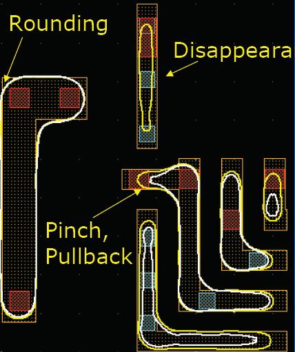
 A key problem is overlay control Double exposures, masks,")

9 Double Patterning Lithography For 22nm and 16nm, the industry most likely will adopt double patterning lithography (DPL) A key problem is overlay control Double exposures, masks, Intelligent CAD solution to compensate unwanted overlay effects or even take advantage of them! [Yang et al, ASPDAC 2010] A new layout decomposition framework Graph-theoretic, multi-objective Stitch mindp 9


10 Issues with DPL Minimum Stitch Insertion Stitch Stitch 1) Yield loss with overlay 2) Area increase due to overlap margin [Lucas SPIE 08] Overlay Compensation 2 nd patterning 2 nd patterning 2 nd patterning 1 st patterning C 1 - C 1 C 2 - C 2 C 1 - C 1 C 2 + C 2 1 st patterning 1 st patterning 1 st patterning 2 nd patterning Without Overlay Compensation With Overlay Compensation 10
11 Comparisons with Previous Works Balanced Density Overlay Compensation Stitch Minimization Complexity [Yao+, ICCAD08] [Yuan+, ISPD09] [Xu+, ICCAD09] Our Framework [ASPDAC10] No No Yes (ILP) No No Yes (ILP) No No Yes (ILP) Yes Yes Yes (Bi-Partitioning) NP-Complete NP-Complete NP-Complete Polynomial Time O(NlogN) 11


12 Benefits of Balanced Density S38584:13% and 87% S38584: 50% and 50% C432:27% and 73% (7 stitches) C432:50% and 50% (17 stitches) 12

 ( Weight=0.")
13 Overlay Compensation Result ( Weight=0.0 ) ( Weight=0.2 ) ( Weight=0.5 ) ( Weight=1.0 ) 13

14 Spacer-type DPL SADP (self-aligned double patterning) Core mask and trim mask Less overlay cf. LELE (1) target (2) core mask (3) sidewall spacer (4) trim mask 14
15 Challenges in SADP A single width of sidewall spacer Does not allow stitch points SADP currently in production only for 1D patterns NAND Flash memory applications SADP for 2D random logic patterns is challenging [Ban et al., DAC 11] proposes systematic techniques to perform layout decomposition for general 2D patterns 15
16 How to Solve Coloring Conflicts? A B C D E Coloring conflict A A C B D F D Grouping E E A F Merging D E 1 st Mask Sidewall Spacer The space/width of the merged region should be equal or larger than the minimum space/width of the trim mask. Trim mask overlay at the merged region 16 cut (open) Trimming


17 22nm Metal1 Standard Cell (1) Target layout (2) Mandrel & spacer (3) Trim mask (4) Final patterns 17
18 Electronic Beam Lithography Maskless technology, which shoots desired patterns directly into a silicon wafer Low throughput is its major hurdle Variable Shaped Beam (VSB) Total number of 11 shots are needed
19 Character Projection (CP) Technology Print some complex shapes in one electronic beam shot, rather than writing multiple rectangles. Electron Gun 3 shots only Electron Gun Shaping aperture Shaping aperture Stencil Wafer Stencil Electron Gun Electron Gun Wafer Character Shaping aperture Shaping aperture Stencil Stencil Wafer Wafer
20 Blank B Blank A BlankB BlankA Min(BlankA, BlankB) Overlapped Characters The number of characters is limited due to the area constraints of the stencil Layout A Spanned region of electron beam from shaping aperture Layout B H h Character w Character A Character B By overlapping adjacent characters/sharing blank spaces, more characters can be put on the stencil W Layout A Layout B Layout A Layout B Character A Character B Character A Character B
21 Not a Trivial Task [Yuan-Pan, ISPD 11] Character candidates to be considered A B C Stencil Order Matters A B C Out of Stencil C B A
22 Stencil Planning and Optimization #shots (projection time) #characters on stencil D-1 1D-2 1D-3 1D-4 0 1D-1 1D-2 1D-3 1D-4 NON-OVERLAP GREEDY PROPOSED NON-OVERLAP GREEDY PROPOSED #CPU(logscale) D-1 1D-2 1D-3 1D-4 NON-OVERLAP GREEDY PROPOSED 51%, 14% reduction on shot number over previous ILP-based approach without overlapping characters and greedy algorithm. 22
23 Outline Introduction Nanolithography for 22nm and Beyond: Double Pattern Lithography Emerging Lithography Some Other Design-Technology Co-optimization Issues NBTI and Clock Network Design 3D Integration: TSV, Stress, Reliability Conclusion 23
24 What is NBTI? NBTI is a key failure mechanism for PMOS Cause PMOS Vth to drift when driven by GND E.g., V TH = +60mV after 10 years 30% increase in inverter delay NBTI-Induced Skew Management in Gated Clock Trees [Chakraborty+, DATE 2009, ISPD 2010] Main problem: clock gating cause inbalance between different clock buffers/receivers Key idea: try to balance NBTI degradation Both circuit design (run time) and CAD techniques (design time) Similar principle holds for PBTI 24
25 Clock Gating Induced V TH Imbalance SP0=50% SP0=50% CLK SP0=50% SP0 = Prob. that net is at logic 0. SP0=50% GATE: 30% SP0=35% Larger V TH Lower V TH Using NAND gate reduces SP0 at output Using NOR gate increases SP0 at output In both cases, V TH mismatch will exist! Skew? 25
26 MUX [Chakraborty+, DATE 2009] CLK NOR Gated at 0 GATE CLK_OUT CLK NAND Gated at 1 SELECT If { GATE = FALSE } CLK_OUT = CLK Else If { SELECT = 0 } CLK_OUT = 0 Else CLK_OUT = 1 26
27 [Chakraborty and Pan, ISPD 10] Determine clock gating NAND/NOR during design Not runtime (less penalty and no SELECT signals) Symbolic SP0 Propagation SP0 Aware Delay Characterization Main idea: Optimally pick NAND and NOR gates for clock gating Symbolic Arrival Time Computation Skew Minimization Formulation (ILP) 27
28 Delay is Function of CLK Gating Assignment DINV(0.5) + X2 * DNAND(0.5) + X2 * DNOR(0.5) + ( X4 * DNAND( X2 * 0.5 ) + X4 * DNOR( X2 * 0.5 ) ) 28
29 Results CKT Solver Time (s) OUR Skew (ps) All NAND (ps) All NOR (ps) 10 Rand. (ps) A B C D E F G H Avg: X 2.19X 1.33X Age the circuit to 10 years Our > Rand > NAND > NOR solution Significantly tightens the skew budget 29
30 3D IC Integration Better Performance Photonics MEMS RF Memory CMOS Massive Bandwidth Reduced Interconnect Delays Power Reduction (Less IO driver) Higher Functionality/Space Heterogeneous Integration Smaller Size 3D Maximizes Space Utilization Lower Cost Lower Cost vs. Next-gen Device Reuse of Proven SIP 30 [Courtesy of Dr. H.-M., Tong, ASE]
31 3D IC Yield Y 1 = Joint Yield Memory Y 2 = Repassivation/RDL Yield Y 3 = Interface Yield Processor ELK/ULK RDL X X X X X X X X X X Y 4 = TSV Yield Y 5 = Interface Yield Y 6 = Repassivation/RDL Yield Y 7 = Joint Yield Y 8 = Joint Yield Y 9 = Substrate Yield Y 10 = Joint Yield Y 1 Y 2 Y 3 Y 4 Y 5 Y 6 Y 7 Y 8 Y 9 Y 10 Overall Yield 99.5% 99.5% 99.5% 99.5% 99.5% 99.5% 99.5% 99.5% 99.5% 99.5% 95.0% 99.5% 99.5% 90.0% 90.0% 90.0% 99.5% 99.5% 99.5% 99.5% 99.5% 70.0% Scrap or Barely Usable Scrap [Courtesy of Dr. H.-M., Tong, ASE]
 Since Cu has larger")

32 Thermal Stress Impact Near TSV CTE : Coefficient of thermal expansion [Dao+, ICICDT 2009] TSV: 250 C ~400 C process (Higher than operating temperature) Since Cu has larger CTE than Si, tensile stress is in Si near TSV. < Tensile stress > < Fast NFET, slow PFET with tensile stress > Cu TSV Silicon [Selvanayagam+, ECTC 08, TAP 09] 32 [H.S. Yang, IEDM 2004]
![Stress Aware Design Flow [Yang+, DAC 10] Pre-placed TSV location Stress estimation induced by TSVs Mobility change ( μ/μ) calculation Verilog netlist Cell characterization with mobility (Cell name](/docs-images/76/73085623/images/33-0.jpg "change in Verilog) Stress aware Verilog netlist Verilog, SPEF merging for 3D STA Liberty file having cell timing with different mobility 3D Timing Analysis with PrimeTime Critical gate selection")
33 Stress Aware Design Flow [Yang+, DAC 10] Pre-placed TSV location Stress estimation induced by TSVs Mobility change ( μ/μ) calculation Verilog netlist Cell characterization with mobility (Cell name change in Verilog) Stress aware Verilog netlist Verilog, SPEF merging for 3D STA Liberty file having cell timing with different mobility 3D Timing Analysis with PrimeTime Critical gate selection Optimized layout with TSV stress 33 TSV stress aware layout optimization
34 Stress Effect on Mobility & Current CMOS (Stress: 200MPa, R=r) NMOS: 0.5 μ ( Ids:+1.5%) PMOS: 0.6 μ ( Ids:+1.8%) Cmos NMOS: 0.75 μ ( Ids:+2.25%) PMOS: -0.1 μ( Ids:-0.3%) Cmos TSV NMOS: μ( Ids:+3%) PMOS: - μ( Ids:-3%) Cmos FS corner Cell characterizations based on distance and orientation are needed 34
 e = +4% ( μ/μ) h = +6% INVX1_P8_N8 ( μ/μ) e = +8% ( μ/μ) h = -8% I2 I4 INVX1_P2_0 ( μ/μ) e =")

35 Cell Instantiation Depending on Location TSV2 TSV1 INVX1_P8_N14 ( μ/μ) e = +8% ( μ/μ) h = -14% I3 TSV2 TSV2 I1 KOZ INVX1_P4_P6 ( μ/μ) e = +4% ( μ/μ) h = +6% INVX1_P8_N8 ( μ/μ) e = +8% ( μ/μ) h = -8% I2 I4 INVX1_P2_0 ( μ/μ) e = +2% ( μ/μ) h = 0% KOZ Indentify hole and electron mobility variation according to TSV induced stress Rename cells based on the mobility Cell naming: INVX1_P8_N8 P8: +8% electron mobility variation N8: -8% hole mobility variation 35
36 Falling Delay Variation Rising Delay Variation Inverter Delay Dependence on Stress 30.0% 0.0% -2.0% 20.0% ( μ/μ)e=0% -4.0% ( μ/μ)h=-22% ( μ/μ)h=0% 10.0% ( μ/μ)e=12% ( μ/μ)e=24% -6.0% ( μ/μ)h=10% 0.0% -8.0% 0% 10% 20% 30% Electron Mobility Variation -10.0% -30% -20% -10% 0% 10% 20% Hole Mobility Variation μe : 0%~24% in our test case Dfalling : up to 7.5% μh : -22%~10% in our test case Drising : more than 20% 36
37 Result: Timing Analysis with Stress TSV Specification Width Landing pad KOZ Height Dielectric Resistance Capacitance 4.14um 4.54um 0.4um 20um 0.2um fF Stress effect on critical paths Circuit #Cells Without TSV stress With TSV stress Difference Longest Delay(ns) TNS(ns) 37 Longest Delay(ns) TNS(ns) Longest Delay(ns) TNS(ns) IDCT 14, % -7.7% , % 1.1% , % 5.7% MAC2 29, % 0.3% ETHERNET 77, % 1.3% RISC 88, % 22.9% B18 103, % -12.4% DES_PERT 109, % -8.1% VGA_LCD 126, % -0.9% B19 168, % -10.2% average 75, , , % -0.8%
38 Result: Timing Optimization Critical path manual optimization (Circuit: 8051) Original Optimized Timing Logic Depth Gate Hole(%) Electron (%) Gate Hole(%) Electron (%) Arc Original Delay(ns) Optimized Delay(ns) Reduction Ratio DFFPOSX1 DFFPOSX1 fall % 1 NOR3X NOR3X rise % 2 AND2X AND2X rise % 3 INVX INVX fall % 4 INVX INVX rise % 5 AND2X AND2X rise % 6 BUFX BUFX rise % 7 AOI22X AOI22X fall % 8 INVX INVX rise % 9 OR2X OR2X1 2 8 rise % 10 OR2X OR2X rise % 11 NOR3X NOR3X fall % 12 NAND3X NAND3X rise % 13 BUFX BUFX rise % 14 OR2X2-8 OR2X2 2 8 rise % 15 AOI22X AOI22X fall % 16 OAI21X OAI21X rise % 17 NOR3X NOR3X fall % 18 AOI21X AOI21X rise % 19 INVX INVX fall % 20 OAI21X OAI21X rise % Path Delay % 38


39 Result: Cell Perturbation Original cell placement After cell perturbation Rising critical optimization with hole contour Falling critical optimization with electron contour
40 TSV Stress/Reliability & EM Issues Consider TSV stress during placement [ICCAD 10] Full-chip TSV stress modeling with multiple TSVs and physical layout optimization issues [Mitra+, ECTC 11] TSV EMI analysis [Pak+, ECTC 11] Due to vast difference is size differences A Current B C D E I H G F
41 Conclusion Some new research problems in nanolithography and design-technology co-optimization Pushing the lithography limits:» double patterning, triple/quadruple patterning» E-beam lithography (stencil planning, e-beam proximity effects)» EUV lithography (flare effects, etc.) Resilient design with built-in compensation and error correction (NBTI/PBTI, overlay effects, etc.) 3D-IC manufacturability and reliability issues Holistic treatment in a vertically integrated manner 41

42 Synergistic Design-Technology Co-opt Need good levers at different levels for designtechnology co-optimization (DTC) Give me a place to stand on, and I can move the earth. - Archimedes Lever DTC lever for your sub- 22nm billion transistor design!
Skew Management of NBTI Impacted Gated Clock Trees
 International Symposium on Physical Design 2010 Skew Management of NBTI Impacted Gated Clock Trees Ashutosh Chakraborty and David Z. Pan ECE Department, University of Texas at Austin ashutosh@cerc.utexas.edu
Design for Manufacturability and Reliability in Extreme CMOS Scaling and Beyond
 Design for Manufacturability and Reliability in Extreme CMOS Scaling and Beyond David Z. Pan Dept. of Electrical and Computer Engineering The University of Texas at Austin http://www.cerc.utexas.edu/utda
Skew Management of NBTI Impacted Gated Clock Trees
 Skew Management of NBTI Impacted Gated Clock Trees Ashutosh Chakraborty ECE Department The University of Texas at Austin Austin, TX 78703, USA ashutosh@cerc.utexas.edu David Z. Pan ECE Department The University
TCAD Modeling of Stress Impact on Performance and Reliability
 TCAD Modeling of Stress Impact on Performance and Reliability Xiaopeng Xu TCAD R&D, Synopsys March 16, 2010 SEMATECH Workshop on Stress Management for 3D ICs using Through Silicon Vias 1 Outline Introduction
NANO-CMOS DESIGN FOR MANUFACTURABILILTY
 NANO-CMOS DESIGN FOR MANUFACTURABILILTY Robust Circuit and Physical Design for Sub-65nm Technology Nodes Ban Wong Franz Zach Victor Moroz An u rag Mittal Greg Starr Andrew Kahng WILEY A JOHN WILEY & SONS,
Chapter 2 Process Variability. Overview. 2.1 Sources and Types of Variations
 Chapter 2 Process Variability Overview Parameter variability has always been an issue in integrated circuits. However, comparing with the size of devices, it is relatively increasing with technology evolution,
Thermal-reliable 3D Clock-tree Synthesis Considering Nonlinear Electrical-thermal-coupled TSV Model
 Thermal-reliable 3D Clock-tree Synthesis Considering Nonlinear Electrical-thermal-coupled TSV Model Yang Shang 1, Chun Zhang 1, Hao Yu 1, Chuan Seng Tan 1, Xin Zhao 2, Sung Kyu Lim 2 1 School of Electrical
Lecture 0: Introduction
 Lecture 0: Introduction Introduction q Integrated circuits: many transistors on one chip q Very Large Scale Integration (VLSI): bucketloads! q Complementary Metal Oxide Semiconductor Fast, cheap, low power
Adding a New Dimension to Physical Design. Sachin Sapatnekar University of Minnesota
 Adding a New Dimension to Physical Design Sachin Sapatnekar University of Minnesota 1 Outline What is 3D about? Why 3D? 3D-specific challenges 3D analysis and optimization 2 Planning a city: Land usage
STATIC TIMING ANALYSIS
 STATIC TIMING ANALYSIS Standard Cell Library NanGate 45 nm Open Cell Library Open-source standard cell library Over 62 different functions ranging from buffers, to scan-able FFs with set and reset, to
Performance and Variability Driven Guidelines for BEOL Layout Decomposition with LELE Double Patterning
 Performance and Variability Driven Guidelines for BEOL Layout Decomposition with LELE Double Patterning Tuck-Boon Chan, Kwangok Jeong and Andrew B. Kahng ECE and CSE Depts., University of California at
AE74 VLSI DESIGN JUN 2015
 Q.2 a. Write down the different levels of integration of IC industry. (4) b. With neat sketch explain briefly PMOS & NMOS enhancement mode transistor. N-MOS enhancement mode transistor:- This transistor
Physical Design of Digital Integrated Circuits (EN0291 S40) Sherief Reda Division of Engineering, Brown University Fall 2006
 Sherief Reda Division of Engineering, Brown University Fall 2006") Physical Design of Digital Integrated Circuits (EN0291 S40) Sherief Reda Division of Engineering, Brown University Fall 2006 1 Lecture 04: Timing Analysis Static timing analysis STA for sequential circuits
Physical Design of Digital Integrated Circuits (EN0291 S40) Sherief Reda Division of Engineering, Brown University Fall 2006 1 Lecture 04: Timing Analysis Static timing analysis STA for sequential circuits
There's Plenty of Room at the Bottom
 There's Plenty of Room at the Bottom 12/29/1959 Feynman asked why not put the entire Encyclopedia Britannica (24 volumes) on a pin head (requires atomic scale recording). He proposed to use electron microscope
Self-study problems and questions Processing and Device Technology, FFF110/FYSD13
 Self-study problems and questions Processing and Device Technology, FFF110/FYSD13 Version 2016_01 In addition to the problems discussed at the seminars and at the lectures, you can use this set of problems
KINGS COLLEGE OF ENGINEERING DEPARTMENT OF ELECTRONICS AND COMMUNICATION ENGINEERING QUESTION BANK
 KINGS COLLEGE OF ENGINEERING DEPARTMENT OF ELECTRONICS AND COMMUNICATION ENGINEERING QUESTION BANK SUBJECT CODE: EC 1354 SUB.NAME : VLSI DESIGN YEAR / SEMESTER: III / VI UNIT I MOS TRANSISTOR THEORY AND
EE410 vs. Advanced CMOS Structures
 EE410 vs. Advanced CMOS Structures Prof. Krishna S Department of Electrical Engineering S 1 EE410 CMOS Structure P + poly-si N + poly-si Al/Si alloy LPCVD PSG P + P + N + N + PMOS N-substrate NMOS P-well
Chapter 2 Fault Modeling
 Chapter 2 Fault Modeling Jin-Fu Li Advanced Reliable Systems (ARES) Lab. Department of Electrical Engineering National Central University Jungli, Taiwan Outline Why Model Faults? Fault Models (Faults)
Lithography Issues in Nano Chip Design and Manufacture
 Lithography Issues in Nano Chip Design and Manufacture Xuan Zeng, Jintao Xue and Wei Cai ASIC & System State Key Lab., Microelectronics Dept., Fudan Univerisity Jan. 7, 2007 Jan. 7, 2007 Challenges and
On Critical Path Selection Based Upon Statistical Timing Models -- Theory and Practice
 On Critical Path Selection Based Upon Statistical Timing Models -- Theory and Practice Jing-Jia Liou, Angela Krstic, Li-C. Wang, and Kwang-Ting Cheng University of California - Santa Barbara Problem Find
Research Challenges and Opportunities. in 3D Integrated Circuits. Jan 30, 2009
 Jan 3, 29 Research Challenges and Opportunities in 3D Integrated Circuits Ankur Jain ankur.jain@freescale.com, ankurjain@stanfordalumni.org Freescale Semiconductor, Inc. 28. 1 What is Three-dimensional
CSE241 VLSI Digital Circuits Winter Lecture 07: Timing II
 CSE241 VLSI Digital Circuits Winter 2003 Lecture 07: Timing II CSE241 L3 ASICs.1 Delay Calculation Cell Fall Cap\Tr 0.05 0.2 0.5 0.01 0.02 0.16 0.30 0.5 2.0 0.04 0.32 0.178 0.08 0.64 0.60 1.20 0.1ns 0.147ns
Robust Clock Tree Synthesis with Timing Yield Optimization for 3D-ICs
 Robust Clock Tree Synthesis with Timing Yield Optimization for 3D-ICs Jae-Seok Yang, Jiwoo Pak, Xin Zhao, Sung Kyu Lim, and David Z. Pan Dept. of ECE, The University of Texas at Austin, TX USA School of
EV Group. Engineered Substrates for future compound semiconductor devices
 EV Group Engineered Substrates for future compound semiconductor devices Engineered Substrates HB-LED: Engineered growth substrates GaN / GaP layer transfer Mobility enhancement solutions: III-Vs to silicon
ELEN0037 Microelectronic IC Design. Prof. Dr. Michael Kraft
 ELEN0037 Microelectronic IC Design Prof. Dr. Michael Kraft Lecture 2: Technological Aspects Technology Passive components Active components CMOS Process Basic Layout Scaling CMOS Technology Integrated
Overlay Aware Interconnect and Timing Variation Modeling for Double Patterning Technology
 Overlay Aware Interconnect and Timing Variation Modeling for Double Patterning Technology Jae-Seok Yang, David Z. Pan Dept. of ECE, The University of Texas at Austin, Austin, Tx 78712 jsyang@cerc.utexas.edu,
Buffered Clock Tree Sizing for Skew Minimization under Power and Thermal Budgets
 Buffered Clock Tree Sizing for Skew Minimization under Power and Thermal Budgets Krit Athikulwongse, Xin Zhao, and Sung Kyu Lim School of Electrical and Computer Engineering Georgia Institute of Technology
Statistical Analysis of BTI in the Presence of Processinduced Voltage and Temperature Variations
 Statistical Analysis of BTI in the Presence of Processinduced Voltage and Temperature Variations Farshad Firouzi, Saman Kiamehr, Mehdi. B. Tahoori INSTITUTE OF COMPUTER ENGINEERING (ITEC) CHAIR FOR DEPENDABLE
FLCC Seminar. Spacer Lithography for Reduced Variability in MOSFET Performance
 1 Seminar Spacer Lithography for Reduced Variability in MOSFET Performance Prof. Tsu-Jae King Liu Electrical Engineering & Computer Sciences Dept. University of California at Berkeley Graduate Student:
Nanoscale CMOS Design Issues
 Nanoscale CMOS Design Issues Jaydeep P. Kulkarni Assistant Professor, ECE Department The University of Texas at Austin jaydeep@austin.utexas.edu Fall, 2017, VLSI-1 Class Transistor I-V Review Agenda Non-ideal
Floating Point Representation and Digital Logic. Lecture 11 CS301
 Floating Point Representation and Digital Logic Lecture 11 CS301 Administrative Daily Review of today s lecture w Due tomorrow (10/4) at 8am Lab #3 due Friday (9/7) 1:29pm HW #5 assigned w Due Monday 10/8
DKDT: A Performance Aware Dual Dielectric Assignment for Tunneling Current Reduction
 DKDT: A Performance Aware Dual Dielectric Assignment for Tunneling Current Reduction Saraju P. Mohanty Dept of Computer Science and Engineering University of North Texas smohanty@cs.unt.edu http://www.cs.unt.edu/~smohanty/
918 IEEE TRANSACTIONS ON COMPUTER-AIDED DESIGN OF INTEGRATED CIRCUITS AND SYSTEMS, VOL. 32, NO. 6, JUNE 2013
 918 IEEE TRANSACTIONS ON COMPUTER-AIDED DESIGN OF INTEGRATED CIRCUITS AND SYSTEMS, VOL. 32, NO. 6, JUNE 2013 Skew Management of NBTI Impacted Gated Clock Trees Ashutosh Chakraborty, Member, IEEE, and David
Chapter 2. Design and Fabrication of VLSI Devices
 Chapter 2 Design and Fabrication of VLSI Devices Jason Cong 1 Design and Fabrication of VLSI Devices Objectives: To study the materials used in fabrication of VLSI devices. To study the structure of devices
Reliability of 3D IC with Via-Middle TSV: Characterization and Modeling
 Reliability of 3D IC with Via-Middle TSV: Characterization and Modeling Victor Moroz *, Munkang Choi *, Geert Van der Plas, Paul Marchal, Kristof Croes, and Eric Beyne * Motivation: Build Reliable 3D IC
Previously. ESE370: Circuit-Level Modeling, Design, and Optimization for Digital Systems. Today. Variation Types. Fabrication
 ESE370: Circuit-Level Modeling, Design, and Optimization for Digital Systems Previously Understand how to model transistor behavior Given that we know its parameters V dd, V th, t OX, C OX, W, L, N A Day
Lecture 9: Clocking, Clock Skew, Clock Jitter, Clock Distribution and some FM
 Lecture 9: Clocking, Clock Skew, Clock Jitter, Clock Distribution and some FM Mark McDermott Electrical and Computer Engineering The University of Texas at Austin 9/27/18 VLSI-1 Class Notes Why Clocking?
Equivalent Circuit Model Extraction for Interconnects in 3D ICs
 Equivalent Circuit Model Extraction for Interconnects in 3D ICs A. Ege Engin Assistant Professor, Department of ECE, San Diego State University Email: aengin@mail.sdsu.edu ASP-DAC, Jan. 23, 213 Outline
ECE 546 Lecture 10 MOS Transistors
 ECE 546 Lecture 10 MOS Transistors Spring 2018 Jose E. Schutt-Aine Electrical & Computer Engineering University of Illinois jesa@illinois.edu NMOS Transistor NMOS Transistor N-Channel MOSFET Built on p-type
EEC 118 Lecture #16: Manufacturability. Rajeevan Amirtharajah University of California, Davis
 EEC 118 Lecture #16: Manufacturability Rajeevan Amirtharajah University of California, Davis Outline Finish interconnect discussion Manufacturability: Rabaey G, H (Kang & Leblebici, 14) Amirtharajah, EEC
Lecture 23. Dealing with Interconnect. Impact of Interconnect Parasitics
 Lecture 23 Dealing with Interconnect Impact of Interconnect Parasitics Reduce Reliability Affect Performance Classes of Parasitics Capacitive Resistive Inductive 1 INTERCONNECT Dealing with Capacitance
Lecture 16: Circuit Pitfalls
 Introduction to CMOS VLSI Design Lecture 16: Circuit Pitfalls David Harris Harvey Mudd College Spring 2004 Outline Pitfalls Detective puzzle Given circuit and symptom, diagnose cause and recommend solution
MOSIS REPORT. Spring MOSIS Report 1. MOSIS Report 2. MOSIS Report 3
 MOSIS REPORT Spring 2010 MOSIS Report 1 MOSIS Report 2 MOSIS Report 3 MOSIS Report 1 Design of 4-bit counter using J-K flip flop I. Objective The purpose of this project is to design one 4-bit counter
Lecture 1: Circuits & Layout
 Lecture 1: Circuits & Layout Outline q A Brief History q CMOS Gate esign q Pass Transistors q CMOS Latches & Flip-Flops q Standard Cell Layouts q Stick iagrams 2 A Brief History q 1958: First integrated
University of Toronto. Final Exam
 University of Toronto Final Exam Date - Apr 18, 011 Duration:.5 hrs ECE334 Digital Electronics Lecturer - D. Johns ANSWER QUESTIONS ON THESE SHEETS USING BACKS IF NECESSARY 1. Equation sheet is on last
EE241 - Spring 2003 Advanced Digital Integrated Circuits
 EE241 - Spring 2003 Advanced Digital Integrated Circuits Lecture 16 Energy-Recovery Circuits SOI Technology and Circuits Optimal EDP Contours 1 Leakage and Switching ELk 2 = ESw Opt L ln d K tech α avg
UNIVERSITY OF CALIFORNIA College of Engineering Department of Electrical Engineering and Computer Sciences. Fall Exam 1
 UNIVERSITY OF CALIFORNIA College of Engineering Department of Electrical Engineering and Computer Sciences EECS 143 Fall 2008 Exam 1 Professor Ali Javey Answer Key Name: SID: 1337 Closed book. One sheet
EECS150 - Digital Design Lecture 26 - Faults and Error Correction. Types of Faults in Digital Designs
 EECS150 - Digital Design Lecture 26 - Faults and Error Correction April 25, 2013 John Wawrzynek 1 Types of Faults in Digital Designs Design Bugs (function, timing, power draw) detected and corrected at
Homework Assignment #5 EE 477 Spring 2017 Professor Parker
 Homework Assignment #5 EE 477 Spring 2017 Professor Parker Question 1: (15%) Compute the worst-case rising and falling RC time constants at point B of the circuit below using the Elmore delay method. Assume
EE371 - Advanced VLSI Circuit Design
 EE371 - Advanced VLSI Circuit Design Midterm Examination May 7, 2002 Name: No. Points Score 1. 18 2. 22 3. 30 TOTAL / 70 In recognition of and in the spirit of the Stanford University Honor Code, I certify
S No. Questions Bloom s Taxonomy Level UNIT-I
 GROUP-A (SHORT ANSWER QUESTIONS) S No. Questions Bloom s UNIT-I 1 Define oxidation & Classify different types of oxidation Remember 1 2 Explain about Ion implantation Understand 1 3 Describe lithography
ECE321 Electronics I
 ECE321 Electronics I Lecture 1: Introduction to Digital Electronics Payman Zarkesh-Ha Office: ECE Bldg. 230B Office hours: Tuesday 2:00-3:00PM or by appointment E-mail: payman@ece.unm.edu Slide: 1 Textbook
7. Combinational Circuits
 7. Combinational Circuits Jacob Abraham Department of Electrical and Computer Engineering The University of Texas at Austin VLSI Design Fall 2017 September 25, 2017 ECE Department, University of Texas
Extending the Era of Moore s Law
 14 nm chip X SEM from www.intel.com/content/dam/www/public/us/en/documents/pdf/foundry/mark bohr 2014 idf presentation.pdf Extending the Era of Moore s Law Tsu Jae King Liu Department of Electrical Engineering
ECE 342 Electronic Circuits. Lecture 6 MOS Transistors
 ECE 342 Electronic Circuits Lecture 6 MOS Transistors Jose E. Schutt-Aine Electrical & Computer Engineering University of Illinois jesa@illinois.edu 1 NMOS Transistor Typically L = 0.1 to 3 m, W = 0.2
Logical Effort: Designing for Speed on the Back of an Envelope David Harris Harvey Mudd College Claremont, CA
 Logical Effort: Designing for Speed on the Back of an Envelope David Harris David_Harris@hmc.edu Harvey Mudd College Claremont, CA Outline o Introduction o Delay in a Logic Gate o Multi-stage Logic Networks
UNIVERSITY OF CALIFORNIA College of Engineering Department of Electrical Engineering and Computer Sciences. Professor Oldham Fall 1999
 UNIVERSITY OF CLIFORNI College of Engineering Department of Electrical Engineering and Computer Sciences Professor Oldham Fall 1999 EECS 40 FINL EXM 13 December 1999 Name: Last, First Student ID: T: Kusuma
Will Reliability Limit Moore s Law?
 Will Reliability Limit Moore s Law? Tony Oates, TSMC 1 Outline Trends Interconnect Transistors Soft Errors in Memory and Logic Conclusions 2 Market Growth Electronic Equipment Revenue ($B) 2,500 2,000
Variation-aware Clock Network Design Methodology for Ultra-Low Voltage (ULV) Circuits
 Circuits") Variation-aware Clock Network Design Methodology for Ultra-Low Voltage (ULV) Circuits Xin Zhao, Jeremy R. Tolbert, Chang Liu, Saibal Mukhopadhyay, and Sung Kyu Lim School of ECE, Georgia Institute of Technology,
Variation-aware Clock Network Design Methodology for Ultra-Low Voltage (ULV) Circuits Xin Zhao, Jeremy R. Tolbert, Chang Liu, Saibal Mukhopadhyay, and Sung Kyu Lim School of ECE, Georgia Institute of Technology,
and V DS V GS V T (the saturation region) I DS = k 2 (V GS V T )2 (1+ V DS )
 I DS = k 2 (V GS V T )2 (1+ V DS )") ECE 4420 Spring 2005 Page 1 FINAL EXAMINATION NAME SCORE /100 Problem 1O 2 3 4 5 6 7 Sum Points INSTRUCTIONS: This exam is closed book. You are permitted four sheets of notes (three of which are your sheets
ECE 4420 Spring 2005 Page 1 FINAL EXAMINATION NAME SCORE /100 Problem 1O 2 3 4 5 6 7 Sum Points INSTRUCTIONS: This exam is closed book. You are permitted four sheets of notes (three of which are your sheets
L ECE 4211 UConn F. Jain Scaling Laws for NanoFETs Chapter 10 Logic Gate Scaling
 L13 04202017 ECE 4211 UConn F. Jain Scaling Laws for NanoFETs Chapter 10 Logic Gate Scaling Scaling laws: Generalized scaling (GS) p. 610 Design steps p.613 Nanotransistor issues (page 626) Degradation
MTJ-Based Nonvolatile Logic-in-Memory Architecture and Its Application
 2011 11th Non-Volatile Memory Technology Symposium @ Shanghai, China, Nov. 9, 20112 MTJ-Based Nonvolatile Logic-in-Memory Architecture and Its Application Takahiro Hanyu 1,3, S. Matsunaga 1, D. Suzuki
EECS150 - Digital Design Lecture 26 Faults and Error Correction. Recap
 EECS150 - Digital Design Lecture 26 Faults and Error Correction Nov. 26, 2013 Prof. Ronald Fearing Electrical Engineering and Computer Sciences University of California, Berkeley (slides courtesy of Prof.
CMPEN 411 VLSI Digital Circuits Spring 2012 Lecture 17: Dynamic Sequential Circuits And Timing Issues
 CMPEN 411 VLSI Digital Circuits Spring 2012 Lecture 17: Dynamic Sequential Circuits And Timing Issues [Adapted from Rabaey s Digital Integrated Circuits, Second Edition, 2003 J. Rabaey, A. Chandrakasan,
Luis Manuel Santana Gallego 31 Investigation and simulation of the clock skew in modern integrated circuits
 Luis Manuel Santana Gallego 31 Investigation and simulation of the clock skew in modern egrated circuits 3. Clock skew 3.1. Definitions For two sequentially adjacent registers, as shown in figure.1, C
From Physics to Power, Performance, and Parasitics
 From Physics to Power, Performance, and Parasitics The GTS-Team Global TCAD Solutions GmbH, Böserndorferstraße 1/12, 1010 Vienna, Austria O. Baumgartner et al. (GTS) GTS 1 / 25 Scales, methods, hierarchies
EECS 141: SPRING 09 MIDTERM 2
 University of California College of Engineering Department of Electrical Engineering and Computer Sciences J. Rabaey WeFr 2-3:30pm We, April 22, 2:00-3:30pm EECS 141: SPRING 09 MIDTERM 2 NAME Last First
EE143 LAB. Professor N Cheung, U.C. Berkeley
 EE143 LAB 1 1 EE143 Equipment in Cory 218 2 Guidelines for Process Integration * A sequence of Additive and Subtractive steps with lateral patterning Processing Steps Si wafer Watch out for materials compatibility
EE115C Winter 2017 Digital Electronic Circuits. Lecture 19: Timing Analysis
 EE115C Winter 2017 Digital Electronic Circuits Lecture 19: Timing Analysis Outline Timing parameters Clock nonidealities (skew and jitter) Impact of Clk skew on timing Impact of Clk jitter on timing Flip-flop-
ESE 570: Digital Integrated Circuits and VLSI Fundamentals
 ESE 570: Digital Integrated Circuits and VLSI Fundamentals Lec 4: January 29, 2019 MOS Transistor Theory, MOS Model Penn ESE 570 Spring 2019 Khanna Lecture Outline! CMOS Process Enhancements! Semiconductor
EUVL Readiness for High Volume Manufacturing
 EUVL Readiness for High Volume Manufacturing Britt Turkot Intel Corporation Outline Exposure Tool Progress Power Availability Intel demo results Reticle Defectivity Pellicle Materials Conclusion 2 Source
Lecture 6: DC & Transient Response
 Lecture 6: DC & Transient Response Slides courtesy of Deming Chen Slides based on the initial set from David Harris CMOS VLSI Design Outline Pass Transistors DC Response Logic Levels and Noise Margins
DC and Transient. Courtesy of Dr. Daehyun Dr. Dr. Shmuel and Dr.
 DC and Transient Courtesy of Dr. Daehyun Lim@WSU, Dr. Harris@HMC, Dr. Shmuel Wimer@BIU and Dr. Choi@PSU http://csce.uark.edu +1 (479) 575-604 yrpeng@uark.edu Pass Transistors We have assumed source is
CMPEN 411 VLSI Digital Circuits Spring Lecture 14: Designing for Low Power
 CMPEN 411 VLSI Digital Circuits Spring 2012 Lecture 14: Designing for Low Power [Adapted from Rabaey s Digital Integrated Circuits, Second Edition, 2003 J. Rabaey, A. Chandrakasan, B. Nikolic] Sp12 CMPEN
Errata of K Introduction to VLSI Systems: A Logic, Circuit, and System Perspective
 Errata of K13126 Introduction to VLSI Systems: A Logic, Circuit, and System Perspective Chapter 1. Page 8, Table 1-1) The 0.35-µm process parameters are from MOSIS, both 0.25-µm and 0.18-µm process parameters
EE371 - Advanced VLSI Circuit Design
 EE371 - Advanced VLSI Circuit Design Midterm Examination May 1999 Name: No. Points Score 1. 20 2. 24 3. 26 4. 20 TOTAL / 90 In recognition of and in the spirit of the Stanford University Honor Code, I
Advanced Flash and Nano-Floating Gate Memories
 Advanced Flash and Nano-Floating Gate Memories Mater. Res. Soc. Symp. Proc. Vol. 1337 2011 Materials Research Society DOI: 10.1557/opl.2011.1028 Scaling Challenges for NAND and Replacement Memory Technology
ESE570 Spring University of Pennsylvania Department of Electrical and System Engineering Digital Integrated Cicruits AND VLSI Fundamentals
 University of Pennsylvania Department of Electrical and System Engineering Digital Integrated Cicruits AND VLSI Fundamentals ESE570, Spring 017 Final Wednesday, May 3 4 Problems with point weightings shown.
Variability Aware Statistical Timing Modelling Using SPICE Simulations
 Variability Aware Statistical Timing Modelling Using SPICE Simulations Master Thesis by Di Wang Informatics and Mathematical Modelling, Technical University of Denmark January 23, 2008 2 Contents List
Xarxes de distribució del senyal de. interferència electromagnètica, consum, soroll de conmutació.
 Xarxes de distribució del senyal de rellotge. Clock skew, jitter, interferència electromagnètica, consum, soroll de conmutació. (transparències generades a partir de la presentació de Jan M. Rabaey, Anantha
Section 12: Intro to Devices
 Section 12: Intro to Devices Extensive reading materials on reserve, including Robert F. Pierret, Semiconductor Device Fundamentals EE143 Ali Javey Bond Model of Electrons and Holes Si Si Si Si Si Si Si
Chapter 9. Estimating circuit speed. 9.1 Counting gate delays
 Chapter 9 Estimating circuit speed 9.1 Counting gate delays The simplest method for estimating the speed of a VLSI circuit is to count the number of VLSI logic gates that the input signals must propagate
ESE 570: Digital Integrated Circuits and VLSI Fundamentals
 ESE 570: Digital Integrated Circuits and VLSI Fundamentals Lec 23: April 17, 2018 I/O Circuits, Inductive Noise, CLK Generation Lecture Outline! Packaging! Variation and Testing! I/O Circuits! Inductive
Microelectronics Part 1: Main CMOS circuits design rules
 GBM8320 Dispositifs Médicaux telligents Microelectronics Part 1: Main CMOS circuits design rules Mohamad Sawan et al. Laboratoire de neurotechnologies Polystim! http://www.cours.polymtl.ca/gbm8320/! med-amine.miled@polymtl.ca!
Technologies VII. Alternative Lithographic PROCEEDINGS OF SPIE. Douglas J. Resnick Christopher Bencher. Sponsored by. Cosponsored by.
 PROCEEDINGS OF SPIE Alternative Lithographic Technologies VII Douglas J. Resnick Christopher Bencher Editors 23-26 February 2015 San Jose, California, United States Sponsored by SPIE Cosponsored by DNS
Lecture 7 Circuit Delay, Area and Power
 Lecture 7 Circuit Delay, Area and Power lecture notes from S. Mitra Intro VLSI System course (EE271) Introduction to VLSI Systems 1 Circuits and Delay Introduction to VLSI Systems 2 Power, Delay and Area:
Today s lecture. EE141- Spring 2003 Lecture 4. Design Rules CMOS Inverter MOS Transistor Model
 - Spring 003 Lecture 4 Design Rules CMOS Inverter MOS Transistor Model Today s lecture Design Rules The CMOS inverter at a glance An MOS transistor model for manual analysis Important! Labs start next
CARNEGIE MELLON UNIVERSITY DEPARTMENT OF ELECTRICAL AND COMPUTER ENGINEERING DIGITAL INTEGRATED CIRCUITS FALL 2002
 CARNEGIE MELLON UNIVERSITY DEPARTMENT OF ELECTRICAL AND COMPUTER ENGINEERING 18-322 DIGITAL INTEGRATED CIRCUITS FALL 2002 Final Examination, Monday Dec. 16, 2002 NAME: SECTION: Time: 180 minutes Closed
ENEE 359a Digital VLSI Design
 SLIDE 1 ENEE 359a Digital VLSI Design Prof. blj@eng.umd.edu Credit where credit is due: Slides contain original artwork ( Jacob 2004) as well as material taken liberally from Irwin & Vijay s CSE477 slides
Exam 2 Fall How does the total propagation delay (T HL +T LH ) for an inverter sized for equal
 for an inverter sized for equal") EE 434 Exam 2 Fall 2006 Name Instructions. Students may bring 2 pages of notes to this exam. There are 10 questions and 5 problems. The questions are worth 2 points each and the problems are all worth
EE 434 Exam 2 Fall 2006 Name Instructions. Students may bring 2 pages of notes to this exam. There are 10 questions and 5 problems. The questions are worth 2 points each and the problems are all worth
VLSI VLSI CIRCUIT DESIGN PROCESSES P.VIDYA SAGAR ( ASSOCIATE PROFESSOR) Department of Electronics and Communication Engineering, VBIT
 Department of Electronics and Communication Engineering, VBIT") VLSI VLSI CIRCUIT DESIGN PROCESSES P.VIDYA SAGAR ( ASSOCIATE PROFESSOR) SYLLABUS UNIT II VLSI CIRCUIT DESIGN PROCESSES: VLSI Design Flow, MOS Layers, Stick Diagrams, Design Rules and Layout, 2 m CMOS Design
VLSI VLSI CIRCUIT DESIGN PROCESSES P.VIDYA SAGAR ( ASSOCIATE PROFESSOR) SYLLABUS UNIT II VLSI CIRCUIT DESIGN PROCESSES: VLSI Design Flow, MOS Layers, Stick Diagrams, Design Rules and Layout, 2 m CMOS Design
! CMOS Process Enhancements. ! Semiconductor Physics. " Band gaps. " Field Effects. ! MOS Physics. " Cut-off. " Depletion.
 ESE 570: Digital Integrated Circuits and VLSI Fundamentals Lec 4: January 9, 019 MOS Transistor Theory, MOS Model Lecture Outline CMOS Process Enhancements Semiconductor Physics Band gaps Field Effects
Design for Manufacturability and Power Estimation. Physical issues verification (DSM)
") Design for Manufacturability and Power Estimation Lecture 25 Alessandra Nardi Thanks to Prof. Jan Rabaey and Prof. K. Keutzer Physical issues verification (DSM) Interconnects Signal Integrity P/G integrity
Design for Manufacturability and Power Estimation Lecture 25 Alessandra Nardi Thanks to Prof. Jan Rabaey and Prof. K. Keutzer Physical issues verification (DSM) Interconnects Signal Integrity P/G integrity
ECE 342 Electronic Circuits. 3. MOS Transistors
 ECE 342 Electronic Circuits 3. MOS Transistors Jose E. Schutt-Aine Electrical & Computer Engineering University of Illinois jschutt@emlab.uiuc.edu 1 NMOS Transistor Typically L = 0.1 to 3 m, W = 0.2 to
Computer-Aided Design for Manufacturability
 Computer-Aided Design for Manufacturability Michael Orshansky UC Berkeley From DSM to DFM A new layer of difficulties on top of the complex physics of DSM Advanced manufacturing introduces new challenges
EE 560 CHIP INPUT AND OUTPUT (I/0) CIRCUITS. Kenneth R. Laker, University of Pennsylvania
 CIRCUITS. Kenneth R. Laker, University of Pennsylvania") 1 EE 560 CHIP INPUT AND OUTPUT (I/0) CIRCUITS 2 -> ESD PROTECTION CIRCUITS (INPUT PADS) -> ON-CHIP CLOCK GENERATION & DISTRIBUTION -> OUTPUT PADS -> ON-CHIP NOISE DUE TO PARASITIC INDUCTANCE -> SUPER BUFFER
1 EE 560 CHIP INPUT AND OUTPUT (I/0) CIRCUITS 2 -> ESD PROTECTION CIRCUITS (INPUT PADS) -> ON-CHIP CLOCK GENERATION & DISTRIBUTION -> OUTPUT PADS -> ON-CHIP NOISE DUE TO PARASITIC INDUCTANCE -> SUPER BUFFER
There s Plenty of Room at the Bottom and at the Top
 14 nm chip X SEM from www.intel.com/content/dam/www/public/us/en/documents/pdf/foundry/mark bohr 2014 idf presentation.pdf There s Plenty of Room at the Bottom and at the Top Tsu Jae King Liu Department
Multiple Gate CMOS and Beyond
 Multiple CMOS and Beyond Dept. of EECS, KAIST Yang-Kyu Choi Outline 1. Ultimate Scaling of MOSFETs - 3nm Nanowire FET - 8nm Non-Volatile Memory Device 2. Multiple Functions of MOSFETs 3. Summary 2 CMOS
EE5780 Advanced VLSI CAD
 EE5780 Advanced VLSI CAD Lecture 4 DC and Transient Responses, Circuit Delays Zhuo Feng 4.1 Outline Pass Transistors DC Response Logic Levels and Noise Margins Transient Response RC Delay Models Delay
Hybrid Wafer Level Bonding for 3D IC
 Hybrid Wafer Level Bonding for 3D IC An Equipment Perspective Markus Wimplinger, Corporate Technology Development & IP Director History & Roadmap - BSI CIS Devices???? 2013 2 nd Generation 3D BSI CIS with