Xarxes de distribució del senyal de. interferència electromagnètica, consum, soroll de conmutació.
|
|
|
- Cecilia Stafford
- 5 years ago
- Views:
Transcription
1 Xarxes de distribució del senyal de rellotge. Clock skew, jitter, interferència electromagnètica, consum, soroll de conmutació. (transparències generades a partir de la presentació de Jan M. Rabaey, Anantha Chandrakasan,i Borivoje Nikolić en el llibre Digital Integrated Circuits, A design perspective ) 1
2 When synchronized circuits are employed a clock signal must be distributed to all of the clocked storage elements in a clock domain with a minimum of skew and jitter. Whether the clock domain is an entire system spanning many cabinets or a small portion of a chip, clock distribution is a difficult problem. Variations in wire delays and driver delays, a non-uniform and possible time-varying clocl load, and noise all add to the uncertainty of the clock 2
3 Synchronous Timing CLK In R Combinational 1 R Logic 2 C in C out Out 3
4 Timing Definitions 4
5 Latch Parameters D Q Clk Clk D PW m t hold T t su Q t c-q t d-q Delays can be different for rising and falling data transitions 5
6 Register Parameters D Q Clk Clk T D t hold t su Q t c-q Delays can be different for rising and falling data transitions 6
7 Clock Uncertainties 4 Power Supply Devices 2 3 Interconnect 6 Capacitive Load 1 Clock Generation 5 Temperature 7 Coupling to Adjacent Lines Sources of clock uncertainty 7
8 Clock Nonidealities Clock skew Spatial variation in temporally equivalent clock edges for 2 given signals; mainly deterministic, t SK Clock jitter Temporal variations in consecutive edges of the same clock signal; random noise Cycle-to-cycle (short-term) t JS Long term t JL Variation of the pulse width Important for level sensitive clocking 8
9 Clock Skew # of registers Earliest occurrence of Clk edge Nominal δ/2 Latest occurrence of Clk edge Nominal + δ /2 Insertion delay Max Clk skew Clk delay δ 9
10 Positive and Negative Skew In R1 D Q Combinational Logic R2 D Q Combinational Logic R3 D Q CLK t CLK1 t CLK2 t CLK3 delay (a) Positive skew delay In R1 D Q Combinational Logic R2 D Q Combinational Logic R3 D Q t CLK1 t CLK2 t CLK3 delay delay CLK (b) Negative skew 10
11 Positive Skew T CLK + δ CLK1 1 δ T CLK 3 CLK2 2 4 δ + t h Launching edge arrives before the receiving edge 11
12 Negative Skew T CLK + δ CLK1 1 T CLK 3 CLK2 2 δ 4 Receiving edge arrives before the launching edge 12
13 Timing Constraints In R1 D Q Combinational Logic R2 D Q CLK t CLK1 t CLK2 t c q t c q, cd t su, t hold t logic t logic, cd Minimum cycle time: T - δ = t c-q + t su + t logic Worst case is when receiving edge arrives early (positive δ) 13
14 Clock Skew and Jitter Clk t SK Clk t JS Both skew and jitter affect the effective cycle time Only skew affects the race margin 14
15 Timing Constraints In R1 D Q Combinational Logic R2 D Q CLK t CLK1 t CLK2 t c q t c q, cd t su, t hold t logic t logic, cd Hold time constraint: t (c-q, cd) + t (logic, cd) > t hold + δ Worst case is when receiving edge arrives late Race between data and clock 15
16 Impact of Jitter 2 T CLK 5 CLK t ji tte r t jitter 6 In REGS CLK t c-q, t c-q, cd t su, t hold t jitter Combinational Logic t logic t logic, cd 16
17 Longest Logic Path in Edge-Triggered Systems Clk T Clk-Q T T LM T SU T JI + δ Latest point of launching Earliest arrival of next cycle 17
18 Clock Constraints in Edge-Triggered Systems If launching edge is late and receiving edge is early, the data will not be too late if: T c-q + T LM + T SU < T T JI,1 T JI,2 - δ Minimum cycle time is determined by the maximum delays through the logic T c-q + T LM + T SU + δ + 2 T JI < T Skew can be either positive or negative 18
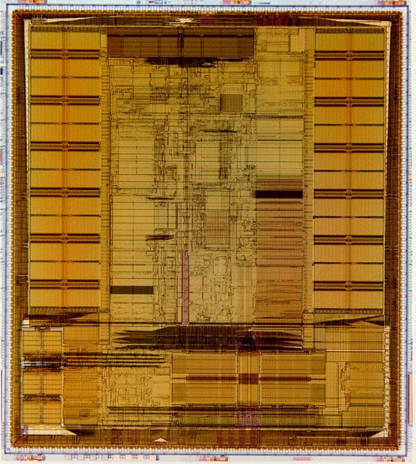
19 How to counter Clock Skew? Negative Skew REG φ REG. REG log Out In REG φ φ Positive Skew φ Clock Distribution Data and Clock Routing 19
20 Sources of Skew and Jitter Sources of Skew and Jitter Clock uncertainty: systematic or random. Clock uncertainty: static or time-varying (1) Clock signal generation (2) Manufacturing device variations (3) Interconnect variations (4) Environmental variations (5) Capacitive coupling (6) Data-dependent clock jitter 20
21 Clock Distribution H-tree 4x4 processor array CLK Clock is distributed in a tree-like fashion 21

22 More realistic H-treeH [Restle98] 22
23 The Grid System Driver GCLK GCLK Driver Driver GCLK No rc-matching Large power Driver GCLK 23
24 Example: DEC Alpha (0.5 µm) Clock Frequency: 300 MHz Million Transistors Total Clock Load: 3.75 nf (dynamic logic) Power in Clock Distribution network : 20 W (out of 50) Uses Two Level Clock Distribution: Single 6-stage driver at center of chip Secondary buffers drive left and right side clock grid in Metal3 and Metal4 Total driver size: 58 cm! 24
25 21164 Clocking t rise = 0.35ns t cycle = 3.3ns Clock waveform final drivers pre-driver Location of clock driver on die t skew = 150ps 2 phase single wire clock, distributed globally 2 distributed driver channels Reduced RC delay/skew Improved thermal distribution 3.75nF clock load 58 cm final driver width Local inverters for latching Conditional clocks in caches to reduce power More complex race checking Device variation 25
26 26

27 Clock Skew in Alpha Processor 27
28 EV6 (Alpha 21264) Clocking 600 MHz 0.35 micron CMOS t cycle = 1.67ns t rise = 0.35ns Global clock waveform t skew = 50ps PLL 2 Phase, with multiple conditional buffered clocks 2.8 nf clock load 40 cm final driver width Local clocks can be gated off to save power Reduced load/skew Reduced thermal issues Multiple clocks complicate race checking 28
29 21264 Clocking 29


30 ps EV6 Clock Results ps GCLK Skew (at Vdd/2 Crossings) GCLK Rise Times (20% to 80% Extrapolated to 0% to 100%) 30
31 EV7 Clock Hierarchy Active Skew Management and Multiple Clock Domains NCLK (Mem Ctrl) + widely dispersed drivers DLL DLL DLL + DLLs compensate static and lowfrequency variation + divides design and verification effort L2L_CLK (L2 Cache) GCLK (CPU Core) PLL L2R_CLK (L2 Cache) - DLL design and verification is added work SYSCLK + tailored clocks 31
, noise coupling")
32 Moreover Clock lines are the most active of the lines in a synchronous system. Consequently they are the main factor for electromagnetic interference (EMI), noise coupling and consumption. 32
EE115C Winter 2017 Digital Electronic Circuits. Lecture 19: Timing Analysis
 EE115C Winter 2017 Digital Electronic Circuits Lecture 19: Timing Analysis Outline Timing parameters Clock nonidealities (skew and jitter) Impact of Clk skew on timing Impact of Clk jitter on timing Flip-flop-
The Linear-Feedback Shift Register
 EECS 141 S02 Timing Project 2: A Random Number Generator R R R S 0 S 1 S 2 1 0 0 0 1 0 1 0 1 1 1 0 1 1 1 0 1 1 0 0 1 1 0 0 The Linear-Feedback Shift Register 1 Project Goal Design a 4-bit LFSR SPEED, SPEED,
Timing Issues. Digital Integrated Circuits A Design Perspective. Jan M. Rabaey Anantha Chandrakasan Borivoje Nikolić. January 2003
 Digital Integrated Circuits A Design Perspective Jan M. Rabaey Anantha Chandrakasan Borivoje Nikolić Timing Issues January 2003 1 Synchronous Timing CLK In R Combinational 1 R Logic 2 C in C out Out 2
GMU, ECE 680 Physical VLSI Design 1
 ECE680: Physical VLSI Design Chapter VII Timing Issues in Digital Circuits (chapter 10 in textbook) GMU, ECE 680 Physical VLSI Design 1 Synchronous Timing (Fig. 10 1) CLK In R Combinational 1 R Logic 2
Lecture 25. Dealing with Interconnect and Timing. Digital Integrated Circuits Interconnect
 Lecture 25 Dealing with Interconnect and Timing Administrivia Projects will be graded by next week Project phase 3 will be announced next Tu.» Will be homework-like» Report will be combined poster Today
Clock signal in digital circuit is responsible for synchronizing the transfer to the data between processing elements.
 1 2 Introduction Clock signal in digital circuit is responsible for synchronizing the transfer to the data between processing elements. Defines the precise instants when the circuit is allowed to change
Lecture 23. Dealing with Interconnect. Impact of Interconnect Parasitics
 Lecture 23 Dealing with Interconnect Impact of Interconnect Parasitics Reduce Reliability Affect Performance Classes of Parasitics Capacitive Resistive Inductive 1 INTERCONNECT Dealing with Capacitance
EECS 427 Lecture 14: Timing Readings: EECS 427 F09 Lecture Reminders
 EECS 427 Lecture 14: Timing Readings: 10.1-10.3 EECS 427 F09 Lecture 14 1 Reminders CA assignments Please submit CA6 by tomorrow noon CA7 is due in a week Seminar by Prof. Bora Nikolic SRAM variability
Lecture 9: Clocking, Clock Skew, Clock Jitter, Clock Distribution and some FM
 Lecture 9: Clocking, Clock Skew, Clock Jitter, Clock Distribution and some FM Mark McDermott Electrical and Computer Engineering The University of Texas at Austin 9/27/18 VLSI-1 Class Notes Why Clocking?
CMPEN 411 VLSI Digital Circuits Spring 2012 Lecture 17: Dynamic Sequential Circuits And Timing Issues
 CMPEN 411 VLSI Digital Circuits Spring 2012 Lecture 17: Dynamic Sequential Circuits And Timing Issues [Adapted from Rabaey s Digital Integrated Circuits, Second Edition, 2003 J. Rabaey, A. Chandrakasan,
Clocking Issues: Distribution, Energy
 EE M216A.:. Fall 2010 Lecture 12 Clocking Issues: istribution, Energy Prof. ejan Marković ee216a@gmail.com Clock istribution Goals: eliver clock to all memory elements with acceptable skew eliver clock
EE241 - Spring 2007 Advanced Digital Integrated Circuits. Announcements
 EE241 - Spring 2007 Advanced Digital Integrated Circuits Lecture 25: Synchronization Timing Announcements Homework 5 due on 4/26 Final exam on May 8 in class Project presentations on May 3, 1-5pm 2 1 Project
Issues on Timing and Clocking
 ECE152B TC 1 Issues on Timing and Clocking X Combinational Logic Z... clock clock clock period ECE152B TC 2 Latch and Flip-Flop L CK CK 1 L1 1 L2 2 CK CK CK ECE152B TC 3 Clocking X Combinational Logic...
Lecture 27: Latches. Final presentations May 8, 1-5pm, BWRC Final reports due May 7 Final exam, Monday, May :30pm, 241 Cory
 EE241 - Spring 2008 Advanced Digital Integrated Circuits Lecture 27: Latches Timing Announcements Wrapping-up the class: Final presentations May 8, 1-5pm, BWRC Final reports due May 7 Final exam, Monday,
Homework 2 due on Wednesday Quiz #2 on Wednesday Midterm project report due next Week (4 pages)
") EE241 - Spring 2013 Advanced Digital Integrated Circuits Lecture 12: SRAM Design ECC Timing Announcements Homework 2 due on Wednesday Quiz #2 on Wednesday Midterm project report due next Week (4 pages)
EE241 - Spring 2013 Advanced Digital Integrated Circuits Lecture 12: SRAM Design ECC Timing Announcements Homework 2 due on Wednesday Quiz #2 on Wednesday Midterm project report due next Week (4 pages)
CSE241 VLSI Digital Circuits Winter Lecture 07: Timing II
 CSE241 VLSI Digital Circuits Winter 2003 Lecture 07: Timing II CSE241 L3 ASICs.1 Delay Calculation Cell Fall Cap\Tr 0.05 0.2 0.5 0.01 0.02 0.16 0.30 0.5 2.0 0.04 0.32 0.178 0.08 0.64 0.60 1.20 0.1ns 0.147ns
Digital System Clocking: High-Performance and Low-Power Aspects. Vojin G. Oklobdzija, Vladimir M. Stojanovic, Dejan M. Markovic, Nikola M.
 Digital System Clocking: High-Performance and Low-Power Aspects Vojin G. Oklobdzija, Vladimir M. Stojanovic, Dejan M. Markovic, Nikola M. Nedovic Wiley-Interscience and IEEE Press, January 2003 Nov. 14,
Digital Integrated Circuits A Design Perspective
 Digital Integrated Circuits A Design Perspective Jan M. Rabaey Anantha Chandrakasan Borivoje Nikolic Designing Sequential Logic Circuits November 2002 Sequential Logic Inputs Current State COMBINATIONAL
EE241 - Spring 2006 Advanced Digital Integrated Circuits
 EE241 - Spring 2006 Advanced Digital Integrated Circuits Lecture 20: Asynchronous & Synchronization Self-timed and Asynchronous Design Functions of clock in synchronous design 1) Acts as completion signal
Jan M. Rabaey Anantha Chandrakasan Borivoje Nikolic. November Digital Integrated Circuits 2nd Sequential Circuits
 igital Integrated Circuits A esign Perspective Jan M. Rabaey Anantha Chandrakasan Borivoje Nikolic esigning i Sequential Logic Circuits November 2002 Sequential Logic Inputs Current State COMBINATIONAL
Digital VLSI Design. Lecture 8: Clock Tree Synthesis
 Digital VLSI Design Lecture 8: Clock Tree Synthesis Semester A, 2018-19 Lecturer: Dr. Adam Teman January 12, 2019 Disclaimer: This course was prepared, in its entirety, by Adam Teman. Many materials were
Itanium TM Processor Clock Design
 Itanium TM Processor Design Utpal Desai 1, Simon Tam, Robert Kim, Ji Zhang, Stefan Rusu Intel Corporation, M/S SC12-502, 2200 Mission College Blvd, Santa Clara, CA 95052 ABSTRACT The Itanium processor
Designing Sequential Logic Circuits
 igital Integrated Circuits (83-313) Lecture 5: esigning Sequential Logic Circuits Semester B, 2016-17 Lecturer: r. Adam Teman TAs: Itamar Levi, Robert Giterman 26 April 2017 isclaimer: This course was
Digital Integrated Circuits A Design Perspective
 igital Integrated Circuits A esign Perspective Jan M. Rabaey Anantha Chandrakasan Borivoje Nikolic esigning Sequential Logic Circuits November 2002 Sequential Logic Inputs Current State COMBINATIONAL LOGIC
Digital Integrated Circuits A Design Perspective
 igital Integrated Circuits A esign Perspective Jan M. Rabaey Anantha Chandrakasan Borivoje Nikolic esigning Sequential Logic Circuits November 2002 Naming Conventions In our text: a latch is level sensitive
ESE 570: Digital Integrated Circuits and VLSI Fundamentals
 ESE 570: Digital Integrated Circuits and VLSI Fundamentals Lec 23: April 17, 2018 I/O Circuits, Inductive Noise, CLK Generation Lecture Outline! Packaging! Variation and Testing! I/O Circuits! Inductive
Implementation of Clock Network Based on Clock Mesh
 International Conference on Information Technology and Management Innovation (ICITMI 2015) Implementation of Clock Network Based on Clock Mesh He Xin 1, a *, Huang Xu 2,b and Li Yujing 3,c 1 Sichuan Institute
Lecture 9: Sequential Logic Circuits. Reading: CH 7
 Lecture 9: Sequential Logic Circuits Reading: CH 7 Sequential Logic FSM (Finite-state machine) Inputs Current State COMBINATIONAL LOGIC Registers Outputs = f(current, inputs) Next state 2 storage mechanisms
UNIVERSITY OF CALIFORNIA
 UNIVERSITY OF CALIFORNIA College of Engineering Department of Electrical Engineering and Computer Sciences Last modified on April 14, 2004 by Brian Leibowitz (bsl@eecs.berkeley.edu) Jan Rabaey Homework
Luis Manuel Santana Gallego 31 Investigation and simulation of the clock skew in modern integrated circuits
 Luis Manuel Santana Gallego 31 Investigation and simulation of the clock skew in modern egrated circuits 3. Clock skew 3.1. Definitions For two sequentially adjacent registers, as shown in figure.1, C
Lecture 21: Packaging, Power, & Clock
 Lecture 21: Packaging, Power, & Clock Outline Packaging Power Distribution Clock Distribution 2 Packages Package functions Electrical connection of signals and power from chip to board Little delay or
EE382 Processor Design Winter 1999 Chapter 2 Lectures Clocking and Pipelining
 Slide 1 EE382 Processor Design Winter 1999 Chapter 2 Lectures Clocking and Pipelining Slide 2 Topics Clocking Clock Parameters Latch Types Requirements for reliable clocking Pipelining Optimal pipelining
Skew-Tolerant Circuit Design
 Skew-Tolerant Circuit Design David Harris David_Harris@hmc.edu December, 2000 Harvey Mudd College Claremont, CA Outline Introduction Skew-Tolerant Circuits Traditional Domino Circuits Skew-Tolerant Domino
CMPEN 411. Spring Lecture 18: Static Sequential Circuits
 CMPEN 411 VLSI Digital Circuits Spring 2011 Lecture 18: Static Sequential Circuits [Adapted from Rabaey s Digital Integrated Circuits, Second Edition, 2003 J. Rabaey, A. Chandrakasan, B. Nikolic] Sp11
Clock Strategy. VLSI System Design NCKUEE-KJLEE
 Clock Strategy Clocked Systems Latch and Flip-flops System timing Clock skew High speed latch design Phase locked loop ynamic logic Multiple phase Clock distribution Clocked Systems Most VLSI systems are
Next, we check the race condition to see if the circuit will work properly. Note that the minimum logic delay is a single sum.
 UNIVERSITY OF CALIFORNIA College of Engineering Department of Electrical Engineering and Computer Sciences Last modified on May 1, 2003 by Dejan Markovic (dejan@eecs.berkeley.edu) Prof. Jan Rabaey EECS
Problem Set 9 Solutions
 CSE 26 Digital Computers: Organization and Logical Design - 27 Jon Turner Problem Set 9 Solutions. For each of the sequential circuits shown below, draw in the missing parts of the timing diagrams. You
UNIVERSITY OF CALIFORNIA, BERKELEY College of Engineering Department of Electrical Engineering and Computer Sciences
 UNIVERSITY OF CALIFORNIA, BERKELEY College of Engineering Department of Electrical Engineering and Computer Sciences Elad Alon Homework #9 EECS141 PROBLEM 1: TIMING Consider the simple state machine shown
Digital Integrated Circuits A Design Perspective. Arithmetic Circuits. Jan M. Rabaey Anantha Chandrakasan Borivoje Nikolic.
 Digital Integrated Circuits A Design Perspective Jan M. Rabaey Anantha Chandrakasan Borivoje Nikolic Arithmetic Circuits January, 2003 1 A Generic Digital Processor MEM ORY INPUT-OUTPUT CONTROL DATAPATH
Timing Analysis with Clock Skew
 , Mark Horowitz 1, & Dean Liu 1 David_Harris@hmc.edu, {horowitz, dliu}@vlsi.stanford.edu March, 1999 Harvey Mudd College Claremont, CA 1 (with Stanford University, Stanford, CA) Outline Introduction Timing
The Wire. Digital Integrated Circuits A Design Perspective. Jan M. Rabaey Anantha Chandrakasan Borivoje Nikolic. July 30, 2002
 Digital Integrated Circuits A Design Perspective Jan M. Rabaey Anantha Chandrakasan Borivoje Nikolic The Wire July 30, 2002 1 The Wire transmitters receivers schematics physical 2 Interconnect Impact on
Circuit A. Circuit B
 UNIVERSITY OF CALIFORNIA College of Engineering Department of Electrical Engineering and Computer Sciences Last modified on November 19, 2006 by Karl Skucha (kskucha@eecs) Borivoje Nikolić Homework #9
Design for Manufacturability and Power Estimation. Physical issues verification (DSM)
") Design for Manufacturability and Power Estimation Lecture 25 Alessandra Nardi Thanks to Prof. Jan Rabaey and Prof. K. Keutzer Physical issues verification (DSM) Interconnects Signal Integrity P/G integrity
Design for Manufacturability and Power Estimation Lecture 25 Alessandra Nardi Thanks to Prof. Jan Rabaey and Prof. K. Keutzer Physical issues verification (DSM) Interconnects Signal Integrity P/G integrity
Jin-Fu Li Advanced Reliable Systems (ARES) Lab. Department of Electrical Engineering. Jungli, Taiwan
 Lab. Department of Electrical Engineering. Jungli, Taiwan") Chapter 7 Sequential Circuits Jin-Fu Li Advanced Reliable Systems (ARES) Lab. epartment of Electrical Engineering National Central University it Jungli, Taiwan Outline Latches & Registers Sequencing Timing
Chapter 7 Sequential Circuits Jin-Fu Li Advanced Reliable Systems (ARES) Lab. epartment of Electrical Engineering National Central University it Jungli, Taiwan Outline Latches & Registers Sequencing Timing
Final presentations May 8, 1-5pm, BWRC Final reports due May 7, 8pm Final exam, Monday, May :30pm, 241 Cory
 EE241 - Spring 2008 Advanced Digital Integrated Circuits Lecture 28: Latch-Based iming Conclusion Announcements Wrapping-up the class: Final presentations May 8, 1-5pm, BWRC Final reports due May 7, 8pm
MODULE III PHYSICAL DESIGN ISSUES
 VLSI Digital Design MODULE III PHYSICAL DESIGN ISSUES 3.2 Power-supply and clock distribution EE - VDD -P2006 3:1 3.1.1 Power dissipation in CMOS gates Power dissipation importance Package Cost. Power
Name: Answers. Mean: 83, Standard Deviation: 12 Q1 Q2 Q3 Q4 Q5 Q6 Total. ESE370 Fall 2015
 University of Pennsylvania Department of Electrical and System Engineering Circuit-Level Modeling, Design, and Optimization for Digital Systems ESE370, Fall 2015 Final Tuesday, December 15 Problem weightings
MASSACHUSETTS INSTITUTE OF TECHNOLOGY Department of Electrical Engineering and Computer Sciences
 MASSACHUSETTS INSTITUTE OF TECHNOLOGY Department of Electrical Engineering and Computer Sciences Analysis and Design of Digital Integrated Circuits (6.374) - Fall 2003 Quiz #2 Prof. Anantha Chandrakasan
EE 560 CHIP INPUT AND OUTPUT (I/0) CIRCUITS. Kenneth R. Laker, University of Pennsylvania
 CIRCUITS. Kenneth R. Laker, University of Pennsylvania") 1 EE 560 CHIP INPUT AND OUTPUT (I/0) CIRCUITS 2 -> ESD PROTECTION CIRCUITS (INPUT PADS) -> ON-CHIP CLOCK GENERATION & DISTRIBUTION -> OUTPUT PADS -> ON-CHIP NOISE DUE TO PARASITIC INDUCTANCE -> SUPER BUFFER
1 EE 560 CHIP INPUT AND OUTPUT (I/0) CIRCUITS 2 -> ESD PROTECTION CIRCUITS (INPUT PADS) -> ON-CHIP CLOCK GENERATION & DISTRIBUTION -> OUTPUT PADS -> ON-CHIP NOISE DUE TO PARASITIC INDUCTANCE -> SUPER BUFFER
Fault Modeling. 李昆忠 Kuen-Jong Lee. Dept. of Electrical Engineering National Cheng-Kung University Tainan, Taiwan. VLSI Testing Class
 Fault Modeling 李昆忠 Kuen-Jong Lee Dept. of Electrical Engineering National Cheng-Kung University Tainan, Taiwan Class Fault Modeling Some Definitions Why Modeling Faults Various Fault Models Fault Detection
Spiral 2 7. Capacitance, Delay and Sizing. Mark Redekopp
 2-7.1 Spiral 2 7 Capacitance, Delay and Sizing Mark Redekopp 2-7.2 Learning Outcomes I understand the sources of capacitance in CMOS circuits I understand how delay scales with resistance, capacitance
CARNEGIE MELLON UNIVERSITY DEPARTMENT OF ELECTRICAL AND COMPUTER ENGINEERING DIGITAL INTEGRATED CIRCUITS FALL 2002
 CARNEGIE MELLON UNIVERSITY DEPARTMENT OF ELECTRICAL AND COMPUTER ENGINEERING 18-322 DIGITAL INTEGRATED CIRCUITS FALL 2002 Final Examination, Monday Dec. 16, 2002 NAME: SECTION: Time: 180 minutes Closed
Last Lecture. Power Dissipation CMOS Scaling. EECS 141 S02 Lecture 8
 EECS 141 S02 Lecture 8 Power Dissipation CMOS Scaling Last Lecture CMOS Inverter loading Switching Performance Evaluation Design optimization Inverter Sizing 1 Today CMOS Inverter power dissipation» Dynamic»
Chapter 5 CMOS Logic Gate Design
 Chapter 5 CMOS Logic Gate Design Section 5. -To achieve correct operation of integrated logic gates, we need to satisfy 1. Functional specification. Temporal (timing) constraint. (1) In CMOS, incorrect
CPE/EE 422/522. Chapter 1 - Review of Logic Design Fundamentals. Dr. Rhonda Kay Gaede UAH. 1.1 Combinational Logic
 CPE/EE 422/522 Chapter - Review of Logic Design Fundamentals Dr. Rhonda Kay Gaede UAH UAH Chapter CPE/EE 422/522. Combinational Logic Combinational Logic has no control inputs. When the inputs to a combinational
Physical Design of Digital Integrated Circuits (EN0291 S40) Sherief Reda Division of Engineering, Brown University Fall 2006
 Sherief Reda Division of Engineering, Brown University Fall 2006") Physical Design of Digital Integrated Circuits (EN0291 S40) Sherief Reda Division of Engineering, Brown University Fall 2006 1 Lecture 04: Timing Analysis Static timing analysis STA for sequential circuits
Physical Design of Digital Integrated Circuits (EN0291 S40) Sherief Reda Division of Engineering, Brown University Fall 2006 1 Lecture 04: Timing Analysis Static timing analysis STA for sequential circuits
Methodology to Achieve Higher Tolerance to Delay Variations in Synchronous Circuits
 Methodology to Achieve Higher Tolerance to Delay Variations in Synchronous Circuits Emre Salman and Eby G. Friedman Department of Electrical and Computer Engineering University of Rochester Rochester,
EEC 118 Lecture #16: Manufacturability. Rajeevan Amirtharajah University of California, Davis
 EEC 118 Lecture #16: Manufacturability Rajeevan Amirtharajah University of California, Davis Outline Finish interconnect discussion Manufacturability: Rabaey G, H (Kang & Leblebici, 14) Amirtharajah, EEC
ALU, Latches and Flip-Flops
 CSE14: Components and Design Techniques for Digital Systems ALU, Latches and Flip-Flops Tajana Simunic Rosing Where we are. Last time: ALUs Plan for today: ALU example, latches and flip flops Exam #1 grades
Statistical Clock Skew Modeling with Data Delay Variations
 Statistical Clock Skew Modeling with Data Delay Variations Abstract David Harris 1 and Sam Naffziger 2 David_Harris@hmc.edu, sdn@fc.hp.com Accurate clock skew budgets are important for microprocessor designers
9/18/2008 GMU, ECE 680 Physical VLSI Design
 ECE680: Physical VLSI esign Chapter IV esigning Sequential Logic Circuits (Chapter 7) 1 Sequential Logic Inputs Current State COMBINATIONAL LOGIC Registers Outputs Next state 2 storage mechanisms positive
ESE 570: Digital Integrated Circuits and VLSI Fundamentals
 ESE 570: Digital Integrated Circuits and VLSI Fundamentals Lec 19: March 29, 2018 Memory Overview, Memory Core Cells Today! Charge Leakage/Charge Sharing " Domino Logic Design Considerations! Logic Comparisons!
Digital Integrated Circuits A Design Perspective. Arithmetic Circuits. Jan M. Rabaey Anantha Chandrakasan Borivoje Nikolic.
 Digital Integrated Circuits A Design Perspective Jan M. Rabaey Anantha Chandrakasan Borivoje Nikolic Arithmetic Circuits January, 2003 1 A Generic Digital Processor MEMORY INPUT-OUTPUT CONTROL DATAPATH
ECE 342 Electronic Circuits. Lecture 35 CMOS Delay Model
 ECE 34 Electronic Circuits Lecture 35 CMOS Delay Model Jose E. Schutt-Aine Electrical & Computer Engineering University of Illinois jesa@illinois.edu ECE 34 Jose Schutt Aine 1 Digital Circuits V IH : Input
Reducing Delay Uncertainty in Deeply Scaled Integrated Circuits Using Interdependent Timing Constraints
 Reducing Delay Uncertainty in Deeply Scaled Integrated Circuits Using Interdependent Timing Constraints Emre Salman and Eby G. Friedman Department of Electrical and Computer Engineering University of Rochester
Chapter 13. Clocked Circuits SEQUENTIAL VS. COMBINATIONAL CMOS TG LATCHES, FLIP FLOPS. Baker Ch. 13 Clocked Circuits. Introduction to VLSI
 Chapter 13 Clocked Circuits SEQUENTIAL VS. COMBINATIONAL CMOS TG LATCHES, FLIP FLOPS SET-RESET (SR) ARBITER LATCHES FLIP FLOPS EDGE TRIGGERED DFF FF TIMING Joseph A. Elias, Ph.D. Adjunct Professor, University
Semiconductor Memories
 Semiconductor References: Adapted from: Digital Integrated Circuits: A Design Perspective, J. Rabaey UCB Principles of CMOS VLSI Design: A Systems Perspective, 2nd Ed., N. H. E. Weste and K. Eshraghian
EE141Microelettronica. CMOS Logic
 Microelettronica CMOS Logic CMOS logic Power consumption in CMOS logic gates Where Does Power Go in CMOS? Dynamic Power Consumption Charging and Discharging Capacitors Short Circuit Currents Short Circuit
C.K. Ken Yang UCLA Courtesy of MAH EE 215B
 Decoders: Logical Effort Applied C.K. Ken Yang UCLA yang@ee.ucla.edu Courtesy of MAH 1 Overview Reading Rabaey 6.2.2 (Ratio-ed logic) W&H 6.2.2 Overview We have now gone through the basics of decoders,
EE241 - Spring 2000 Advanced Digital Integrated Circuits. Announcements
 EE241 - Spring 2000 Advanced Digital Integrated Circuits Lecture 3 Circuit Optimization for Speed Announcements Tu 2/8/00 class will be pre-taped on Friday, 2/4, 4-5:30 203 McLaughlin Class notes are available
CMOS Inverter. Performance Scaling
 Announcements Exam #2 regrade requests due today. Homework #8 due today. Final Exam: Th June 12, 8:30 10:20am, CMU 120 (extension to 11:20am requested). Grades available for viewing via Catalyst. CMOS
! Charge Leakage/Charge Sharing. " Domino Logic Design Considerations. ! Logic Comparisons. ! Memory. " Classification. " ROM Memories.
 ESE 57: Digital Integrated Circuits and VLSI Fundamentals Lec 9: March 9, 8 Memory Overview, Memory Core Cells Today! Charge Leakage/ " Domino Logic Design Considerations! Logic Comparisons! Memory " Classification
9/18/2008 GMU, ECE 680 Physical VLSI Design
 ECE680: Physical VLSI Design Chapter III CMOS Device, Inverter, Combinational circuit Logic and Layout Part 3 Combinational Logic Gates (textbook chapter 6) 9/18/2008 GMU, ECE 680 Physical VLSI Design
CMOS logic gates. João Canas Ferreira. March University of Porto Faculty of Engineering
 CMOS logic gates João Canas Ferreira University of Porto Faculty of Engineering March 2016 Topics 1 General structure 2 General properties 3 Cell layout João Canas Ferreira (FEUP) CMOS logic gates March
Signal integrity in deep-sub-micron integrated circuits
 Signal integrity in deep-sub-micron integrated circuits Alessandro Bogliolo abogliolo@ing.unife.it Outline Introduction General signaling scheme Noise sources and effects in DSM ICs Supply noise Synchronization
GMU, ECE 680 Physical VLSI Design
 ECE680: Physical VLSI esign Chapter IV esigning Sequential Logic Circuits (Chapter 7) 1 Sequential Logic Inputs Current State COMBINATIONAL LOGIC Registers Outputs Next state 2 storage mechanisms positive
Digital Integrated Circuits A Design Perspective
 Semiconductor Memories Adapted from Chapter 12 of Digital Integrated Circuits A Design Perspective Jan M. Rabaey et al. Copyright 2003 Prentice Hall/Pearson Outline Memory Classification Memory Architectures
EEC 216 Lecture #3: Power Estimation, Interconnect, & Architecture. Rajeevan Amirtharajah University of California, Davis
 EEC 216 Lecture #3: Power Estimation, Interconnect, & Architecture Rajeevan Amirtharajah University of California, Davis Outline Announcements Review: PDP, EDP, Intersignal Correlations, Glitching, Top
MODULE 5 Chapter 7. Clocked Storage Elements
 MODULE 5 Chapter 7 Clocked Storage Elements 3/9/2015 1 Outline Background Clocked Storage Elements Timing, terminology, classification Static CSEs Latches Registers Dynamic CSEs Latches Registers 3/9/2015
THE INVERTER. Inverter
 THE INVERTER DIGITAL GATES Fundamental Parameters Functionality Reliability, Robustness Area Performance» Speed (delay)» Power Consumption» Energy Noise in Digital Integrated Circuits v(t) V DD i(t) (a)
Stop Watch (System Controller Approach)
") Stop Watch (System Controller Approach) Problem Design a stop watch that can measure times taken for two events Inputs CLK = 6 Hz RESET: Asynchronously reset everything X: comes from push button First
Stop Watch (System Controller Approach) Problem Design a stop watch that can measure times taken for two events Inputs CLK = 6 Hz RESET: Asynchronously reset everything X: comes from push button First
TAU' Low-power CMOS clock drivers. Mircea R. Stan, Wayne P. Burleson.
 TAU'95 149 Low-power CMOS clock drivers Mircea R. Stan, Wayne P. Burleson mstan@risky.ecs.umass.edu, burleson@galois.ecs.umass.edu http://www.ecs.umass.edu/ece/vspgroup/index.html Abstract The clock tree
Very Large Scale Integration (VLSI)
") Very Large Scale Integration (VLSI) Lecture 4 Dr. Ahmed H. Madian Ah_madian@hotmail.com Dr. Ahmed H. Madian-VLSI Contents Delay estimation Simple RC model Penfield-Rubenstein Model Logical effort Delay
Very Large Scale Integration (VLSI) Lecture 4 Dr. Ahmed H. Madian Ah_madian@hotmail.com Dr. Ahmed H. Madian-VLSI Contents Delay estimation Simple RC model Penfield-Rubenstein Model Logical effort Delay
ΗΜΥ 307 ΨΗΦΙΑΚΑ ΟΛΟΚΛΗΡΩΜΕΝΑ ΚΥΚΛΩΜΑΤΑ Εαρινό Εξάμηνο 2018
 ΗΜΥ 307 ΨΗΦΙΑΚΑ ΟΛΟΚΛΗΡΩΜΕΝΑ ΚΥΚΛΩΜΑΤΑ Εαρινό Εξάμηνο 2018 ΔΙΑΛΕΞΕΙΣ 12-13: esigning ynamic and Static CMOS Sequential Circuits ΧΑΡΗΣ ΘΕΟΧΑΡΙΔΗΣ (ttheocharides@ucy.ac.cy) (ack: Prof. Mary Jane Irwin and
Toward More Accurate Scaling Estimates of CMOS Circuits from 180 nm to 22 nm
 Toward More Accurate Scaling Estimates of CMOS Circuits from 180 nm to 22 nm Aaron Stillmaker, Zhibin Xiao, and Bevan Baas VLSI Computation Lab Department of Electrical and Computer Engineering University
ESE 570: Digital Integrated Circuits and VLSI Fundamentals
 ESE 570: Digital Integrated Circuits and VLSI Fundamentals Lec 21: April 4, 2017 Memory Overview, Memory Core Cells Penn ESE 570 Spring 2017 Khanna Today! Memory " Classification " ROM Memories " RAM Memory
LOGIC CIRCUITS. Basic Experiment and Design of Electronics. Ho Kyung Kim, Ph.D.
 Basic Experiment and Design of Electronics LOGIC CIRCUITS Ho Kyung Kim, Ph.D. hokyung@pusan.ac.kr School of Mechanical Engineering Pusan National University Digital IC packages TTL (transistor-transistor
EECS 151/251A Homework 5
 EECS 151/251A Homework 5 Due Monday, March 5 th, 2018 Problem 1: Timing The data-path shown below is used in a simple processor. clk rd1 rd2 0 wr regfile 1 0 ALU REG 1 The elements used in the design have
Chapter 7. Sequential Circuits Registers, Counters, RAM
 Chapter 7. Sequential Circuits Registers, Counters, RAM Register - a group of binary storage elements suitable for holding binary info A group of FFs constitutes a register Commonly used as temporary storage
Efficient Circuit Analysis under Multiple Input Switching (MIS) Anupama R. Subramaniam
 Anupama R. Subramaniam") Efficient Circuit Analysis under Multiple Input Switching (MIS) by Anupama R. Subramaniam A Dissertation Presented in Partial Fulfillment of the Requirements for the Degree Doctor of Philosophy Approved
Efficient Circuit Analysis under Multiple Input Switching (MIS) by Anupama R. Subramaniam A Dissertation Presented in Partial Fulfillment of the Requirements for the Degree Doctor of Philosophy Approved
Hold Time Illustrations
 Hold Time Illustrations EE213-L09-Sequential Logic.1 Pingqiang, ShanghaiTech, 2018 Hold Time Illustrations EE213-L09-Sequential Logic.2 Pingqiang, ShanghaiTech, 2018 Hold Time Illustrations EE213-L09-Sequential
Lecture 6 Power Zhuo Feng. Z. Feng MTU EE4800 CMOS Digital IC Design & Analysis 2010
 EE4800 CMOS Digital IC Design & Analysis Lecture 6 Power Zhuo Feng 6.1 Outline Power and Energy Dynamic Power Static Power 6.2 Power and Energy Power is drawn from a voltage source attached to the V DD
EE115C Digital Electronic Circuits Homework #4
 EE115 Digital Electronic ircuits Homework #4 Problem 1 Power Dissipation Solution Vdd =1.0V onsider the source follower circuit used to drive a load L =20fF shown above. M1 and M2 are both NMOS transistors
University of Toronto. Final Exam
 University of Toronto Final Exam Date - Apr 18, 011 Duration:.5 hrs ECE334 Digital Electronics Lecturer - D. Johns ANSWER QUESTIONS ON THESE SHEETS USING BACKS IF NECESSARY 1. Equation sheet is on last
EE 447 VLSI Design. Lecture 5: Logical Effort
 EE 447 VLSI Design Lecture 5: Logical Effort Outline Introduction Delay in a Logic Gate Multistage Logic Networks Choosing the Best Number of Stages Example Summary EE 4475: VLSI Logical Design Effort
COMP 103. Lecture 16. Dynamic Logic
 COMP 03 Lecture 6 Dynamic Logic Reading: 6.3, 6.4 [ll lecture notes are adapted from Mary Jane Irwin, Penn State, which were adapted from Rabaey s Digital Integrated Circuits, 2002, J. Rabaey et al.] COMP03
ESE 570: Digital Integrated Circuits and VLSI Fundamentals
 ESE 570: Digital Integrated Circuits and VLSI Fundamentals Lec 24: April 19, 2018 Crosstalk and Wiring, Transmission Lines Lecture Outline! Crosstalk! Repeaters in Wiring! Transmission Lines " Where transmission
ECE321 Electronics I
 ECE321 Electronics I Lecture 1: Introduction to Digital Electronics Payman Zarkesh-Ha Office: ECE Bldg. 230B Office hours: Tuesday 2:00-3:00PM or by appointment E-mail: payman@ece.unm.edu Slide: 1 Textbook
EE141-Fall 2011 Digital Integrated Circuits
 EE4-Fall 20 Digital Integrated Circuits Lecture 5 Memory decoders Administrative Stuff Homework #6 due today Project posted Phase due next Friday Project done in pairs 2 Last Lecture Last lecture Logical
School of EECS Seoul National University
 4!4 07$ 8902808 3 School of EECS Seoul National University Introduction Low power design 3974/:.9 43 Increasing demand on performance and integrity of VLSI circuits Popularity of portable devices Low power