Magnetic tunnel junction beyond memory from logic to neuromorphic computing WANJUN PARK DEPT. OF ELECTRONIC ENGINEERING, HANYANG UNIVERSITY
|
|
|
- Shannon Pierce
- 6 years ago
- Views:
Transcription

1 Magnetic tunnel junction beyond memory from logic to neuromorphic computing WANJUN PARK DEPT. OF ELECTRONIC ENGINEERING, HANYANG UNIVERSITY
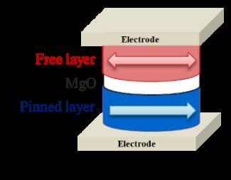
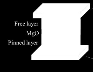
 Tunneling barrier (Insulator: MgO) Pinned layer (FM 2) Bit")


2 Magnetic Tunnel Junctions (MTJs) Structure High density memory Free layer (FM 1) Tunneling barrier (Insulator: MgO) Pinned layer (FM 2) Bit line (BL) Word line (WL) AP or P state 0 or 1 Function Representation of non-volatile binary state according to magnetization configuration Source line (SL) 1 Transistor + 1 MTJ Advantage Scalability Low energy High speed High endurance CMOS compatibility 1GB STT-MRAM, Everspin (2016) - 2 -
3 Content To find computing functions beyond memory from MTJ for integrated circuits Construction of 2-input MTJ MTJ Logic gates Neuromorphic computing Artificial MTJ neuron Artificial MTJ synapse Artificial Neurotransmission system - 3 -


 switching (spin")
4 Basic configuration of MTJ Single input configuration for switching to achieve the binary state FM 1 FM 2 MTJ switching FM 1 FM 2 Anti-parallel state (R AP ) Parallel state (R P ) Methods for magnetization reversal of free layer Switching variable 1: magnetic field switching (current induced Ampere field) I Switching variable 2: Spin-transfer torque (STT) switching (spin polarized current) I - 4 -
 switching - Thermally assisted switching (TAS) I OF -")
5 Two-input configuration of MTJ Motivation for multiple input extension Increase of functional flexibility - Reduction of switching stress by breakup of biases - Increase of switching bias margin Physical variables for MTJ switching H in by applying I AF V in for I STT R MTJ - Ampere field-induce switching - Spin-transfer torque (STT) switching - Thermally assisted switching (TAS) I OF - Voltage-assisted switching (ME effect) - Spin-orbit torque (SOT) switching Multiple input is available for MTJ I STT X I AF Structure of 2-input MTJ Our choice: STT & Ampere field for two switching inputs Sharing integration methods developed for MRAM - 5 -
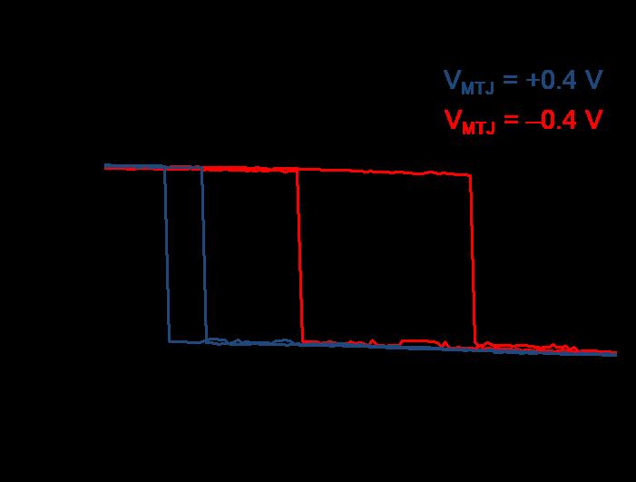
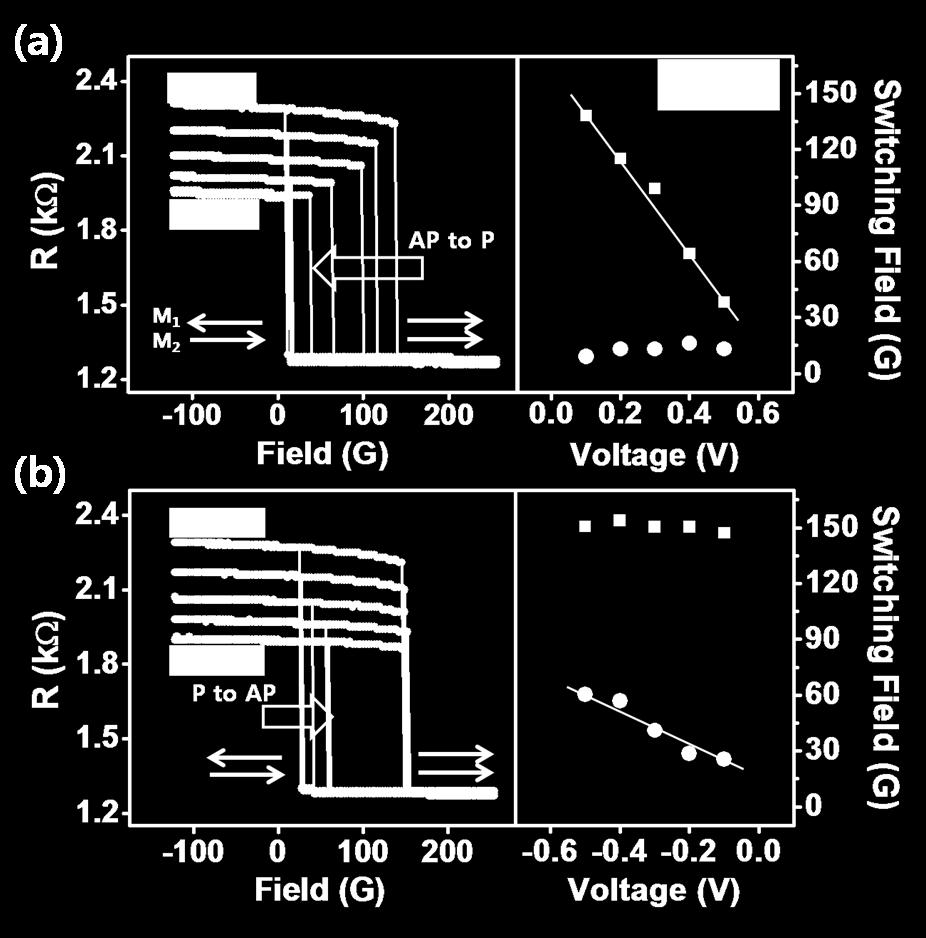
6 Switching characteristics of 2-input MTJ MTJs for switching characteristics due to mixed inputs of STT & Ampere field Size : (80 80) ~ ( ) nm 2-6 -
 H a = 30 Oe H")

 : Required energy for STT")


7 Interpretation of 2-input switching H a = 0 (at coercive center) H a = 30 Oe H a = -30 Oe Magnetic field assisted STT switching Case for switching to be P state Energy due to Ampere field (H ext = H a ) : Required energy for STT switching E b+ = E b0 - E b * H s : Switching field E 0 : Energy barrier at zero magnetic field a J : Spin transfer torque a c : Critical spin transfer torque β = 2-7 -

, V H =0.")
, V H =0.")
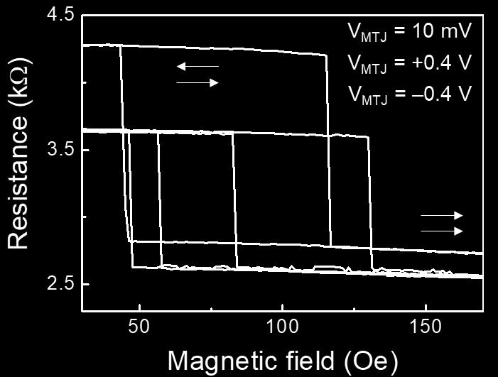
8 NAND/NOR representation Definition of binary states for each input Assignment of input values to the STT input terminal Logic value Input 1 (V) Input 2 (H) MTJ OUT 1 V H H H R AP 0 V L H L R P V H R V L =0.2 V(<V S1 ), V H =0.3 V (V S1 <V H <V S2 ) H L =-5 (Oe), H H = 5 (Oe) V H R V L =0.3 V (V S1 <V L <V S2 ), V H =0.4 V (>V S2 ) H L =-5 (Oe), H H = 5 (Oe) - 8 -
9 All logical representation founded in MTJ 7 Boolean logic representations from possible 12 binary inputs of voltage biases for the STT switching No. Initial Input set Input (V, H), Output (R) Logic function State V L V H H L H H (V L,H L ) (V H,H L ) (V L,H H ) (V H,H H ) R AP = 1, R P = 0 R AP = 0, R P = R AP R AP R AP R P NAND AND R AP R P R P R P NOR OR R R AP R P R AP R P NOT V V 4 AP R AP R AP R AP R AP TRUE FALSE R AP R AP R P R P NOT H H R 5 Oe 5 Oe P R P R P R P FALSE TRUE R P R AP R P R P V NIMP H V IMP H R AP R AP R P R AP H IMP V H NIMP V R R P R AP R P R AP V NIMP H V IMP H 10 P R P R P R P R P FALSE TRUE R AP R AP R P R P NOT H H R AP R AP R AP R AP TRUE FALSE - 9 -
10 MTJ Logic gate Logic gate for digital computing - Cascading computing Full schematic of a logic gate


11 14 Boolean functions computed in MTJ logic gate - Each function is confirmed by SPICE simulation modified with MTJ micro-model - XOR and XNOR are missing among full 16 Boolean logics

12 XOR/XNOR MTJ Logic gate - XOR/XNOR gate could be completed by using cascading computing Conclusively, we have two types of MTJ logic gate which allow any digital computing


13 Reconfigurable Logic Reconfigurability: further advantage of MTJ logic < Truth table >


14 Practical example for reconfigurable Logic Carry-out function with reconfigurable logic < Truth table >

15 Neurotransmission spike signal carrying information < Slowly Adapting> < Fast Adapting > Stimulus for tactile sense Pressure Frequency Slowly Adapting Fast Adapting


16 Neural coding Neural (Biological) coding To find carrier for information according to Strength and frequency of input stimulus - Rate coding Information spiking rate - Temporal coding Information Spiking pattern (Spike ordering in timing) - Time-to-first-spike, Phase Correlations, Spiking sequence, Synchrony etc

 ~ E S Toggling between AP and P state")

17 Telegraphic switching Telegraphic switching by mixed effect of STT & Ampere field in 2-inpt MTJ I = -10 µa μa H = 80 Oe R (kω) μa 10 μa 20 μa Time (s) Total Energy (E M + E STT ) ~ E S Toggling between AP and P state Stochastic characteristic Switching probability P(H, I) is defined as the carried information M. Pufall et al., Phys. Rev. B (2004)
 =")
 RRRRRRRR MMMMMM =")
 = 1+ exp( α H +")

18 Rate coding Construction of neural coding : Rate coding RRRRRRRR(BBBBBBBBBBBBBB) = nn ssss (nnnnnnnnnnnn oooo ssssssssssss TT (tttttttt wwwwwwwwwwww) RRRRRRRR MMMMMM = ) tt AAAA (oooo tt PP ) TT (tttttttttt bbbbbb oooo P AP 1 ( H, I) = 1+ exp( α H + βi + γ ) Information carrier : rate Stimulus : H and I applied by independent inputs
19 Artificial neuron function MTJ-based neuron architecture representing the rate coding


 generation (when the")


20 Neurotransmission Neuron system connected by Synapse (Spike-rate-dependent plasticity) Neuron # : 10 11~12 Synapse # : 10 14~ ~4 /neuron - Spike(=Action potential) generation (when the signal is above threshold) - Neural coding Information is coded through spike train Rate coding - Synaptic weight: plasticity for connection strength - Weight modulation Potentiation / Depression Spike-timing-dependent plasticity (STDP)
21 Memristive character of MTJ

22 MTJ-based artificial synapse Construction of input signal for Spike-timing dependent plasticity <Biological STDP> Δt > 0 Δt < 0 R. Froemke et al., Nature (2002)


23 Artificial neurotransmission Neurotransmission system Artificial neurotransmission system MTJs are commonly used for neural and synaptic functions Learning rule of Spike-rate dependent plasticity is possibly applied
24 SRDP learning rule
25 Summary MTJ was modified with two inputs for switching to achieve functional flexibility. Then we found various computing functions for digital to neuromorphic computing
NEUROMORPHIC COMPUTING WITH MAGNETO-METALLIC NEURONS & SYNAPSES: PROSPECTS AND PERSPECTIVES
 NEUROMORPHIC COMPUTING WITH MAGNETO-METALLIC NEURONS & SYNAPSES: PROSPECTS AND PERSPECTIVES KAUSHIK ROY ABHRONIL SENGUPTA, KARTHIK YOGENDRA, DELIANG FAN, SYED SARWAR, PRIYA PANDA, GOPAL SRINIVASAN, JASON
From Spin Torque Random Access Memory to Spintronic Memristor. Xiaobin Wang Seagate Technology
 From Spin Torque Random Access Memory to Spintronic Memristor Xiaobin Wang Seagate Technology Contents Spin Torque Random Access Memory: dynamics characterization, device scale down challenges and opportunities
Experiment 7: Magnitude comparators
 Module: Logic Design Lab Name:... University no:.. Group no: Lab Partner Name: Experiment 7: Magnitude comparators Mr. Mohamed El-Saied Objective: Realization of -bit comparator using logic gates. Realization
A Perpendicular Spin Torque Switching based MRAM for the 28 nm Technology Node
 A Perpendicular Spin Torque Switching based MRAM for the 28 nm Technology Node U.K. Klostermann 1, M. Angerbauer 1, U. Grüning 1, F. Kreupl 1, M. Rührig 2, F. Dahmani 3, M. Kund 1, G. Müller 1 1 Qimonda
XOR - XNOR Gates. The graphic symbol and truth table of XOR gate is shown in the figure.
 XOR - XNOR Gates Lesson Objectives: In addition to AND, OR, NOT, NAND and NOR gates, exclusive-or (XOR) and exclusive-nor (XNOR) gates are also used in the design of digital circuits. These have special
A 68 Parallel Row Access Neuromorphic Core with 22K Multi-Level Synapses Based on Logic- Compatible Embedded Flash Memory Technology
 A 68 Parallel Row Access Neuromorphic Core with 22K Multi-Level Synapses Based on Logic- Compatible Embedded Flash Memory Technology M. Kim 1, J. Kim 1, G. Park 1, L. Everson 1, H. Kim 1, S. Song 1,2,
Perpendicular MTJ stack development for STT MRAM on Endura PVD platform
 Perpendicular MTJ stack development for STT MRAM on Endura PVD platform Mahendra Pakala, Silicon Systems Group, AMAT Dec 16 th, 2014 AVS 2014 *All data in presentation is internal Applied generated data
Solid-State Electronics
 Solid-State Electronics 84 (2013) 191 197 Contents lists available at SciVerse ScienceDirect Solid-State Electronics journal homepage: www.elsevier.com/locate/sse Implication logic gates using spin-transfer-torque-operated
Page 1. A portion of this study was supported by NEDO.
 MRAM : Materials and Devices Current-induced Domain Wall Motion High-speed MRAM N. Ishiwata NEC Corporation Page 1 A portion of this study was supported by NEDO. Outline Introduction Positioning and direction
XI STANDARD [ COMPUTER SCIENCE ] 5 MARKS STUDY MATERIAL.
![XI STANDARD [ COMPUTER SCIENCE ] 5 MARKS STUDY MATERIAL.](/thumbs/81/84726747.jpg "XI STANDARD [ COMPUTER SCIENCE ] 5 MARKS STUDY MATERIAL.") 2017-18 XI STANDARD [ COMPUTER SCIENCE ] 5 MARKS STUDY MATERIAL HALF ADDER 1. The circuit that performs addition within the Arithmetic and Logic Unit of the CPU are called adders. 2. A unit that adds two
2017-18 XI STANDARD [ COMPUTER SCIENCE ] 5 MARKS STUDY MATERIAL HALF ADDER 1. The circuit that performs addition within the Arithmetic and Logic Unit of the CPU are called adders. 2. A unit that adds two
Author : Fabrice BERNARD-GRANGER September 18 th, 2014
 Author : September 18 th, 2014 Spintronic Introduction Spintronic Design Flow and Compact Modelling Process Variation and Design Impact Semiconductor Devices Characterisation Seminar 2 Spintronic Introduction
MTJ-Based Nonvolatile Logic-in-Memory Architecture and Its Application
 2011 11th Non-Volatile Memory Technology Symposium @ Shanghai, China, Nov. 9, 20112 MTJ-Based Nonvolatile Logic-in-Memory Architecture and Its Application Takahiro Hanyu 1,3, S. Matsunaga 1, D. Suzuki
Center for Spintronic Materials, Interfaces, and Novel Architectures. Spintronics Enabled Efficient Neuromorphic Computing: Prospects and Perspectives
 Center for Spintronic Materials, Interfaces, and Novel Architectures Spintronics Enabled Efficient Neuromorphic Computing: Prospects and Perspectives KAUSHIK ROY ABHRONIL SENGUPTA, KARTHIK YOGENDRA, DELIANG
Memory and computing beyond CMOS
 Memory and computing beyond CMOS Dipartimento di Elettronica, Informazione e Bioingegneria Politecnico di Milano daniele.ielmini@polimi.it Outline 2 Introduction What is CMOS? What comes after CMOS? Example:
Digital Logic. Lecture 5 - Chapter 2. Outline. Other Logic Gates and their uses. Other Logic Operations. CS 2420 Husain Gholoom - lecturer Page 1
 Lecture 5 - Chapter 2 Outline Other Logic Gates and their uses Other Logic Operations CS 2420 Husain Gholoom - lecturer Page 1 Digital logic gates CS 2420 Husain Gholoom - lecturer Page 2 Buffer A buffer
RE-ENGINEERING COMPUTING WITH NEURO- MIMETIC DEVICES, CIRCUITS, AND ALGORITHMS
 RE-ENGINEERING COMPUTING WITH NEURO- MIMETIC DEVICES, CIRCUITS, AND ALGORITHMS Kaushik Roy Abhronil Sengupta, Gopal Srinivasan, Aayush Ankit, Priya Panda, Xuanyao Fong, Deliang Fan, Jason Allred School
Additional Gates COE 202. Digital Logic Design. Dr. Muhamed Mudawar King Fahd University of Petroleum and Minerals
 Additional Gates COE 202 Digital Logic Design Dr. Muhamed Mudawar King Fahd University of Petroleum and Minerals Presentation Outline Additional Gates and Symbols Universality of NAND and NOR gates NAND-NAND
Neuromorphic computing with Memristive devices. NCM group
 Neuromorphic computing with Memristive devices NCM group Why neuromorphic? New needs for computing Recognition, Mining, Synthesis (Intel) Increase of Fault (nanoscale engineering) SEMICONDUCTOR TECHNOLOGY
Introduction to Computer Engineering ECE 203
 Introduction to Computer Engineering ECE 203 Northwestern University Department of Electrical Engineering and Computer Science Teacher: Robert Dick Office: L477 Tech Email: dickrp@ece.northwestern.edu
This document is an author-formatted work. The definitive version for citation appears as:
 This document is an author-formatted work. The definitive version for citation appears as: A. Roohi, R. Zand, D. Fan and R. F. DeMara, "Voltage-based Concatenatable Full Adder using Spin Hall Effect Switching,"
SPICE Modeling of STT-RAM for Resilient Design. Zihan Xu, Ketul Sutaria, Chengen Yang, Chaitali Chakrabarti, Yu (Kevin) Cao School of ECEE, ASU
 Cao School of ECEE, ASU") SPICE odeling of STT-RA for Resilient Design Zihan Xu, Ketul Sutaria, Chengen Yang, Chaitali Chakrabarti, Yu (Kevin) Cao School of ECEE, ASU OUTLINE - 2 - Heterogeneous emory Design A Promising Candidate:
SPICE odeling of STT-RA for Resilient Design Zihan Xu, Ketul Sutaria, Chengen Yang, Chaitali Chakrabarti, Yu (Kevin) Cao School of ECEE, ASU OUTLINE - 2 - Heterogeneous emory Design A Promising Candidate:
Gates and Flip-Flops
 Gates and Flip-Flops Chris Kervick (11355511) With Evan Sheridan and Tom Power December 2012 On a scale of 1 to 10, how likely is it that this question is using binary?...4? What s a 4? Abstract The operation
Hopfield Neural Network and Associative Memory. Typical Myelinated Vertebrate Motoneuron (Wikipedia) Topic 3 Polymers and Neurons Lecture 5
 Topic 3 Polymers and Neurons Lecture 5") Hopfield Neural Network and Associative Memory Typical Myelinated Vertebrate Motoneuron (Wikipedia) PHY 411-506 Computational Physics 2 1 Wednesday, March 5 1906 Nobel Prize in Physiology or Medicine.
Hopfield Neural Network and Associative Memory Typical Myelinated Vertebrate Motoneuron (Wikipedia) PHY 411-506 Computational Physics 2 1 Wednesday, March 5 1906 Nobel Prize in Physiology or Medicine.
Novel VLSI Implementation for Triplet-based Spike-Timing Dependent Plasticity
 Novel LSI Implementation for Triplet-based Spike-Timing Dependent Plasticity Mostafa Rahimi Azghadi, Omid Kavehei, Said Al-Sarawi, Nicolangelo Iannella, and Derek Abbott Centre for Biomedical Engineering,
Nonvolatile CMOS Circuits Using Magnetic Tunnel Junction
 November 3-4, 2011 Berkeley, CA, USA Nonvolatile CMOS Circuits Using Magnetic Tunnel Junction Hideo Ohno 1,2 1 Center for Spintronics Integrated Systems, Tohoku University, Japan 2 Laboratory for Nanoelectronics
Kaushik Roy Department of Electrical and Computer Engineering, Purdue University, West Lafayette, IN https://engineering.purdue.edu/nrl/index.
 Beyond Charge-Based Computing: STT- MRAMs Kaushik Roy Department of Electrical and Computer Engineering, Purdue University, West Lafayette, IN https://engineering.purdue.edu/nrl/index.html 1 Failure probability
Floating Point Representation and Digital Logic. Lecture 11 CS301
 Floating Point Representation and Digital Logic Lecture 11 CS301 Administrative Daily Review of today s lecture w Due tomorrow (10/4) at 8am Lab #3 due Friday (9/7) 1:29pm HW #5 assigned w Due Monday 10/8
Addressing Challenges in Neuromorphic Computing with Memristive Synapses
 Addressing Challenges in Neuromorphic Computing with Memristive Synapses Vishal Saxena 1, Xinyu Wu 1 and Maria Mitkova 2 1 Analog Mixed-Signal and Photonic IC (AMPIC) Lab 2 Nanoionic Materials and Devices
Digital Circuits. 1. Inputs & Outputs are quantized at two levels. 2. Binary arithmetic, only digits are 0 & 1. Position indicates power of 2.
 Digital Circuits 1. Inputs & Outputs are quantized at two levels. 2. inary arithmetic, only digits are 0 & 1. Position indicates power of 2. 11001 = 2 4 + 2 3 + 0 + 0 +2 0 16 + 8 + 0 + 0 + 1 = 25 Digital
Wouldn t it be great if
 IDEMA DISKCON Asia-Pacific 2009 Spin Torque MRAM with Perpendicular Magnetisation: A Scalable Path for Ultra-high Density Non-volatile Memory Dr. Randall Law Data Storage Institute Agency for Science Technology
Lecture 6 NEW TYPES OF MEMORY
 Lecture 6 NEW TYPES OF MEMORY Memory Logic needs memory to function (efficiently) Current memories Volatile memory SRAM DRAM Non-volatile memory (Flash) Emerging memories Phase-change memory STT-MRAM (Ferroelectric
CPE100: Digital Logic Design I
 Professor Brendan Morris, SEB 3216, brendan.morris@unlv.edu CPE100: Digital Logic Design I Midterm01 Review http://www.ee.unlv.edu/~b1morris/cpe100/ 2 Logistics Thursday Oct. 5 th In normal lecture (13:00-14:15)
Switches: basic element of physical implementations
 Combinational logic Switches Basic logic and truth tables Logic functions Boolean algebra Proofs by re-writing and by perfect induction Winter 200 CSE370 - II - Boolean Algebra Switches: basic element
Digital Logic. CS211 Computer Architecture. l Topics. l Transistors (Design & Types) l Logic Gates. l Combinational Circuits.
 l Logic Gates. l Combinational Circuits.") CS211 Computer Architecture Digital Logic l Topics l Transistors (Design & Types) l Logic Gates l Combinational Circuits l K-Maps Figures & Tables borrowed from:! http://www.allaboutcircuits.com/vol_4/index.html!
CS211 Computer Architecture Digital Logic l Topics l Transistors (Design & Types) l Logic Gates l Combinational Circuits l K-Maps Figures & Tables borrowed from:! http://www.allaboutcircuits.com/vol_4/index.html!
Cs302 Quiz for MID TERM Exam Solved
 Question # 1 of 10 ( Start time: 01:30:33 PM ) Total Marks: 1 Caveman used a number system that has distinct shapes: 4 5 6 7 Question # 2 of 10 ( Start time: 01:31:25 PM ) Total Marks: 1 TTL based devices
Digital Electronics Part 1: Binary Logic
 Digital Electronics Part 1: Binary Logic Electronic devices in your everyday life What makes these products examples of electronic devices? What are some things they have in common? 2 How do electronics
A Technology-Agnostic MTJ SPICE Model with User-Defined Dimensions for STT-MRAM Scalability Studies
 A Technology-Agnostic MTJ SPICE Model with User-Defined Dimensions for STT-MRAM Scalability Studies Model download website: mtj.umn.edu Jongyeon Kim 1, An Chen 2, Behtash Behin-Aein 2, Saurabh Kumar 1,
Embedded MRAM Technology For logic VLSI Application
 2011 11th Non-Volatile Memory Technology Symposium Embedded MRAM Technology For logic VLSI Application November 7, 2011 Naoki Kasai 1, Shoji Ikeda 1,2, Takahiro Hanyu 1,3, Tetsuo Endoh 1,4, and Hideo Ohno
Quasi Analog Formal Neuron and Its Learning Algorithm Hardware
 Quasi Analog Formal Neuron and Its Learning Algorithm Hardware Karen Nazaryan Division of Microelectronics and Biomedical Devices, State Engineering University of Armenia, 375009, Terian Str. 105, Yerevan,
Digital Logic (2) Boolean Algebra
 Boolean Algebra") Digital Logic (2) Boolean Algebra Boolean algebra is the mathematics of digital systems. It was developed in 1850 s by George Boole. We will use Boolean algebra to minimize logic expressions. Karnaugh
Digital Logic (2) Boolean Algebra Boolean algebra is the mathematics of digital systems. It was developed in 1850 s by George Boole. We will use Boolean algebra to minimize logic expressions. Karnaugh
ECE 342 Electronic Circuits. Lecture 34 CMOS Logic
 ECE 34 Electronic Circuits Lecture 34 CMOS Logic Jose E. Schutt-Aine Electrical & Computer Engineering University of Illinois jesa@illinois.edu 1 De Morgan s Law Digital Logic - Generalization ABC... ABC...
Implementation of Boolean Logic by Digital Circuits
 Implementation of Boolean Logic by Digital Circuits We now consider the use of electronic circuits to implement Boolean functions and arithmetic functions that can be derived from these Boolean functions.
Computer organization
 Computer organization Levels of abstraction Assembler Simulator Applications C C++ Java High-level language SOFTWARE add lw ori Assembly language Goal 0000 0001 0000 1001 0101 Machine instructions/data
Unit 8A Computer Organization. Boolean Logic and Gates
 Unit 8A Computer Organization Boolean Logic and Gates Announcements Bring ear buds or headphones to lab! 15110 Principles of Computing, Carnegie Mellon University - CORTINA 2 Representing and Manipulating
An Overview of Spin-based Integrated Circuits
 ASP-DAC 2014 An Overview of Spin-based Integrated Circuits Wang Kang, Weisheng Zhao, Zhaohao Wang, Jacques-Olivier Klein, Yue Zhang, Djaafar Chabi, Youguang Zhang, Dafiné Ravelosona, and Claude Chappert
Low Energy Spin Transfer Torque RAM (STT-RAM / SPRAM) Zach Foresta April 23, 2009
 Zach Foresta April 23, 2009") Low Energy Spin Transfer Torque RAM (STT-RAM / SPRAM) Zach Foresta April 23, 2009 Overview Background A brief history GMR and why it occurs TMR structure What is spin transfer? A novel device A future
Low Energy Spin Transfer Torque RAM (STT-RAM / SPRAM) Zach Foresta April 23, 2009 Overview Background A brief history GMR and why it occurs TMR structure What is spin transfer? A novel device A future
Introduction to CMOS VLSI Design Lecture 1: Introduction
 Introduction to CMOS VLSI Design Lecture 1: Introduction David Harris, Harvey Mudd College Kartik Mohanram and Steven Levitan University of Pittsburgh Introduction Integrated circuits: many transistors
MRAM: Device Basics and Emerging Technologies
 MRAM: Device Basics and Emerging Technologies Matthew R. Pufall National Institute of Standards and Technology 325 Broadway, Boulder CO 80305-3337 Phone: +1-303-497-5206 FAX: +1-303-497-7364 E-mail: pufall@boulder.nist.gov
Spin-Based Logic and Memory Technologies for Low-Power Systems
 Spin-Based Logic and Memory Technologies for Low-Power Systems A DISSERTATION SUBMITTED TO THE FACULTY OF THE GRADUATE SCHOOL OF THE UNIVERSITY OF MINNESOTA BY Jongyeon Kim IN PARTIAL FULFILLMENT OF THE
Chapter 2 Combinational Logic Circuits
 Logic and Computer Design Fundamentals Chapter 2 Combinational Logic Circuits Part 3 Additional Gates and Circuits Overview Part 1 Gate Circuits and Boolean Equations Binary Logic and Gates Boolean Algebra
Synaptic Devices and Neuron Circuits for Neuron-Inspired NanoElectronics
 Synaptic Devices and Neuron Circuits for Neuron-Inspired NanoElectronics Byung-Gook Park Inter-university Semiconductor Research Center & Department of Electrical and Computer Engineering Seoul National
New Approaches to Reducing Energy Consumption of MRAM write cycles, Ultra-high efficient writing (Voltage-Control) Spintronics Memory (VoCSM)
 Spintronics Memory (VoCSM)") New Approaches to Reducing Energy Consumption of MRAM write cycles, Ultra-high efficient writing (Voltage-Control) Spintronics Memory (VoCSM) Hiroaki Yoda Corporate Research & Development Center, Toshiba
New Approaches to Reducing Energy Consumption of MRAM write cycles, Ultra-high efficient writing (Voltage-Control) Spintronics Memory (VoCSM) Hiroaki Yoda Corporate Research & Development Center, Toshiba
Designing Information Devices and Systems II Spring 2018 J. Roychowdhury and M. Maharbiz Discussion 1A
 EEC 16B esigning Information evices and ystems II pring 2018 J. Roychowdhury and M. Maharbiz iscussion 1A 1 igit Bases (N) p is used to indicate that the number N is expressed in base p. For example, (N)
Computer Organization: Boolean Logic
 Computer Organization: Boolean Logic Representing and Manipulating Data Last Unit How to represent data as a sequence of bits How to interpret bit representations Use of levels of abstraction in representing
2.0 Basic Elements of a Quantum Information Processor. 2.1 Classical information processing The carrier of information
 QSIT09.L03 Page 1 2.0 Basic Elements of a Quantum Information Processor 2.1 Classical information processing 2.1.1 The carrier of information - binary representation of information as bits (Binary digits).
University of Toronto. Final Exam
 University of Toronto Final Exam Date - Apr 18, 011 Duration:.5 hrs ECE334 Digital Electronics Lecturer - D. Johns ANSWER QUESTIONS ON THESE SHEETS USING BACKS IF NECESSARY 1. Equation sheet is on last
Chapter 2 Combinational Logic Circuits
 Logic and Computer Design Fundamentals Chapter 2 Combinational Logic Circuits Part 3 Additional Gates and Circuits Charles Kime & Thomas Kaminski 2008 Pearson Education, Inc. (Hyperlinks are active in
Low Energy SPRAM. Figure 1 Spin valve GMR device hysteresis curve showing states of parallel (P)/anti-parallel (AP) poles,
/anti-parallel (AP) poles,") Zachary Foresta Nanoscale Electronics 04-22-2009 Low Energy SPRAM Introduction The concept of spin transfer was proposed by Slonczewski [1] and Berger [2] in 1996. They stated that when a current of polarized
Zachary Foresta Nanoscale Electronics 04-22-2009 Low Energy SPRAM Introduction The concept of spin transfer was proposed by Slonczewski [1] and Berger [2] in 1996. They stated that when a current of polarized
Test System Requirements For Wafer Level MRAM Test
 Test System Requirements For Wafer Level MRAM Test Raphael Robertazzi IBM/Infineon MRAM Development Alliance With Acknowledgement To Cascade Microtech Inc. And Temptronics Inc. 6/07/04 SWTW-2004 Page [1]
Learning Objectives 10/7/2010. CE 411 Digital System Design. Fundamental of Logic Design. Review the basic concepts of logic circuits. Dr.
 /7/ CE 4 Digital ystem Design Dr. Arshad Aziz Fundamental of ogic Design earning Objectives Review the basic concepts of logic circuits Variables and functions Boolean algebra Minterms and materms ogic
CMSC 313 Lecture 17. Focus Groups. Announcement: in-class lab Thu 10/30 Homework 3 Questions Circuits for Addition Midterm Exam returned
 Focus Groups CMSC 33 Lecture 7 Need good sample of all types of CS students Mon /7 & Thu /2, 2:3p-2:p & 6:p-7:3p Announcement: in-class lab Thu /3 Homework 3 Questions Circuits for Addition Midterm Exam
4 Switching Algebra 4.1 Axioms; Signals and Switching Algebra
 4 Switching Algebra 4.1 Axioms; Signals and Switching Algebra To design a digital circuit that will perform a required function, it is necessary to manipulate and combine the various input signals in certain
MESL: Proposal for a Non-volatile Cascadable Magneto-Electric Spin Logic
 MESL: Proposal for a Non-volatile Cascadable Magneto-Electric Spin Logic Akhilesh Jaiswal 1,, and Kaushik Roy 1 1 School of Electrical and Computer Engineering, Purdue University, West Lafayette, IN, 47907,
SOLID STATE ELECTRONICS DIGITAL ELECTRONICS SOFT CONDENSED MATTER PHYSICS
 SOLID STATE ELECTRONICS DIGITAL ELECTRONICS SOFT CONDENSED MATTER PHYSICS The energy band occupied by the valence electrons is called valence band and is the highest filled band. Bnd occupied by the electrons
Total Time = 90 Minutes, Total Marks = 50. Total /50 /10 /18
 University of Waterloo Department of Electrical & Computer Engineering E&CE 223 Digital Circuits and Systems Midterm Examination Instructor: M. Sachdev October 23rd, 2007 Total Time = 90 Minutes, Total
ECE 545 Digital System Design with VHDL Lecture 1. Digital Logic Refresher Part A Combinational Logic Building Blocks
 ECE 545 Digital System Design with VHDL Lecture Digital Logic Refresher Part A Combinational Logic Building Blocks Lecture Roadmap Combinational Logic Basic Logic Review Basic Gates De Morgan s Law Combinational
Fundamentals of Digital Design
 Fundamentals of Digital Design Digital Radiation Measurement and Spectroscopy NE/RHP 537 1 Binary Number System The binary numeral system, or base-2 number system, is a numeral system that represents numeric
EE 230 Lecture 31. THE MOS TRANSISTOR Model Simplifcations THE Bipolar Junction TRANSISTOR
 EE 23 Lecture 3 THE MOS TRANSISTOR Model Simplifcations THE Bipolar Junction TRANSISTOR Quiz 3 Determine I X. Assume W=u, L=2u, V T =V, uc OX = - 4 A/V 2, λ= And the number is? 3 8 5 2? 6 4 9 7 Quiz 3
Center for Spintronic Materials, Interfaces, and Novel Architectures. Voltage Controlled Antiferromagnetics and Future Spin Memory
 Center for Spintronic Materials, Interfaces, and Novel Architectures Voltage Controlled Antiferromagnetics and Future Spin Memory Maxim Tsoi The University of Texas at Austin Acknowledgments: H. Seinige,
The N3XT Technology for. Brain-Inspired Computing
 The N3XT Technology for Brain-Inspired Computing SystemX Alliance 27..8 Department of Electrical Engineering 25.4.5 2 25.4.5 Source: Google 3 25.4.5 Source: vrworld.com 4 25.4.5 Source: BDC Stanford Magazine
A nanoparticle-organic memory field-effect transistor behaving as a programmable spiking synapse
 A nanoparticle-organic memory field-effect transistor behaving as a programmable spiking synapse F. Alibart,. Pleutin, D. Guerin, K. Lmimouni, D. Vuillaume Molecular Nanostructures & Devices group, Institute
ECE 545 Digital System Design with VHDL Lecture 1A. Digital Logic Refresher Part A Combinational Logic Building Blocks
 ECE 545 Digital System Design with VHDL Lecture A Digital Logic Refresher Part A Combinational Logic Building Blocks Lecture Roadmap Combinational Logic Basic Logic Review Basic Gates De Morgan s Laws
Chapter 2: Boolean Algebra and Logic Gates
 Chapter 2: Boolean Algebra and Logic Gates Mathematical methods that simplify binary logics or circuits rely primarily on Boolean algebra. Boolean algebra: a set of elements, a set of operators, and a
EGC221: Digital Logic Lab
 Division of Engineering Programs EGC221: Digital Logic Lab Experiment #1 Basic Logic Gate Simulation Student s Name: Student s Name: Reg. no.: Reg. no.: Semester: Fall 2016 Date: 07 September 2016 Assessment:
Bipolar Junction Transistor (BJT) - Introduction
 - Introduction") Bipolar Junction Transistor (BJT) - Introduction It was found in 1948 at the Bell Telephone Laboratories. It is a three terminal device and has three semiconductor regions. It can be used in signal amplification
Bipolar Junction Transistor (BJT) - Introduction It was found in 1948 at the Bell Telephone Laboratories. It is a three terminal device and has three semiconductor regions. It can be used in signal amplification
NEM Relay Design for Compact, Ultra-Low-Power Digital Logic Circuits
 NEM Relay Design for Compact, Ultra-Low-Power Digital Logic Circuits T.-J. K. Liu 1, N. Xu 1, I.-R. Chen 1, C. Qian 1, J. Fujiki 2 1 Dept. of Electrical Engineering and Computer Sciences University of
arxiv: v1 [cond-mat.mtrl-sci] 28 Jul 2008
![arxiv: v1 [cond-mat.mtrl-sci] 28 Jul 2008](/thumbs/88/117898456.jpg "arxiv: v1 [cond-mat.mtrl-sci] 28 Jul 2008") Current induced resistance change of magnetic tunnel junctions with ultra-thin MgO tunnel barriers Patryk Krzysteczko, 1, Xinli Kou, 2 Karsten Rott, 1 Andy Thomas, 1 and Günter Reiss 1 1 Bielefeld University,
Current induced resistance change of magnetic tunnel junctions with ultra-thin MgO tunnel barriers Patryk Krzysteczko, 1, Xinli Kou, 2 Karsten Rott, 1 Andy Thomas, 1 and Günter Reiss 1 1 Bielefeld University,
Simple Neural Nets For Pattern Classification
 CHAPTER 2 Simple Neural Nets For Pattern Classification Neural Networks General Discussion One of the simplest tasks that neural nets can be trained to perform is pattern classification. In pattern classification
Simple Neural Nets for Pattern Classification: McCulloch-Pitts Threshold Logic CS 5870
 Simple Neural Nets for Pattern Classification: McCulloch-Pitts Threshold Logic CS 5870 Jugal Kalita University of Colorado Colorado Springs Fall 2014 Logic Gates and Boolean Algebra Logic gates are used
Machine Learning. Neural Networks. (slides from Domingos, Pardo, others)
") Machine Learning Neural Networks (slides from Domingos, Pardo, others) For this week, Reading Chapter 4: Neural Networks (Mitchell, 1997) See Canvas For subsequent weeks: Scaling Learning Algorithms toward
Machine Learning Neural Networks (slides from Domingos, Pardo, others) For this week, Reading Chapter 4: Neural Networks (Mitchell, 1997) See Canvas For subsequent weeks: Scaling Learning Algorithms toward
NTE74LS181 Integrated Circuit TTL Arithmetic Logic Unit/Function Generator
 NTE74LS181 Integrated Circuit TTL Arithmetic Logic Unit/Function Generator Description: The NTE74LS181 is an arithmetic logic unit (ALU)/function generator in a 24 Lead DIP type package that has the complexity
EC/EE DIGITAL ELECTRONICS
 EC/EE 214(R-15) Total No. of Questions :09] [Total No. of Pages : 02 II/IV B.Tech. DEGREE EXAMINATIONS, DECEMBER- 2016 First Semester EC/EE DIGITAL ELECTRONICS Time: Three Hours 1. a) Define Encoder Answer
Logic Gates and Boolean Algebra
 Logic Gates and oolean lgebra The ridge etween Symbolic Logic nd Electronic Digital Computing Compiled y: Muzammil hmad Khan mukhan@ssuet.edu.pk asic Logic Functions and or nand nor xor xnor not 2 Logic
EE141-Fall 2011 Digital Integrated Circuits
 EE4-Fall 20 Digital Integrated Circuits Lecture 5 Memory decoders Administrative Stuff Homework #6 due today Project posted Phase due next Friday Project done in pairs 2 Last Lecture Last lecture Logical
ECE521 Lectures 9 Fully Connected Neural Networks
 ECE521 Lectures 9 Fully Connected Neural Networks Outline Multi-class classification Learning multi-layer neural networks 2 Measuring distance in probability space We learnt that the squared L2 distance
Neural Networks Introduction CIS 32
 Neural Networks Introduction CIS 32 Functionalia Office Hours (Last Change!) - Location Moved to 0317 N (Bridges Room) Today: Alpha-Beta Example Neural Networks Learning with T-R Agent (from before) direction
School of Computer Science and Electrical Engineering 28/05/01. Digital Circuits. Lecture 14. ENG1030 Electrical Physics and Electronics
 Digital Circuits 1 Why are we studying digital So that one day you can design something which is better than the... circuits? 2 Why are we studying digital or something better than the... circuits? 3 Why
F14 Memory Circuits. Lars Ohlsson
 Lars Ohlsson 2018-10-18 F14 Memory Circuits Outline Combinatorial vs. sequential logic circuits Analogue multivibrator circuits Noise in digital circuits CMOS latch CMOS SR flip flop 6T SRAM cell 1T DRAM
Reification of Boolean Logic
 526 U1180 neural networks 1 Chapter 1 Reification of Boolean Logic The modern era of neural networks began with the pioneer work of McCulloch and Pitts (1943). McCulloch was a psychiatrist and neuroanatomist;
Thermal Magnetic Random Access Memory
 Thermal Magnetic andom Access Memory IEEE International Conference on Computer Design New Memory Technologies San Jose, CA October 4, 2005 James Deak NVE Corporation Participants Jim Daughton - PI Art
Applications of Memristors in ANNs
 Applications of Memristors in ANNs Outline Brief intro to ANNs Firing rate networks Single layer perceptron experiment Other (simulation) examples Spiking networks and STDP ANNs ANN is bio inpsired inpsired
Chapter 2 (Lect 2) Canonical and Standard Forms. Standard Form. Other Logic Operators Logic Gates. Sum of Minterms Product of Maxterms
 Canonical and Standard Forms. Standard Form. Other Logic Operators Logic Gates. Sum of Minterms Product of Maxterms") Chapter 2 (Lect 2) Canonical and Standard Forms Sum of Minterms Product of Maxterms Standard Form Sum of products Product of sums Other Logic Operators Logic Gates Basic and Multiple Inputs Positive and
Chapter 2 (Lect 2) Canonical and Standard Forms Sum of Minterms Product of Maxterms Standard Form Sum of products Product of sums Other Logic Operators Logic Gates Basic and Multiple Inputs Positive and
CIRCUITS AND ELECTRONICS. The Digital Abstraction
 6.002 CIRCUITS AND ELECTRONICS The Digital Abstraction Review Discretize matter by agreeing to observe the lumped matter discipline Lumped Circuit Abstraction Analysis tool kit: KVL/KCL, node method, superposition,
Boolean algebra. Examples of these individual laws of Boolean, rules and theorems for Boolean algebra are given in the following table.
 The Laws of Boolean Boolean algebra As well as the logic symbols 0 and 1 being used to represent a digital input or output, we can also use them as constants for a permanently Open or Closed circuit or
Intro To Digital Logic
 Intro To Digital Logic 1 Announcements... Project 2.2 out But delayed till after the midterm Midterm in a week Covers up to last lecture + next week's homework & lab Nick goes "H-Bomb of Justice" About
EECS150 - Digital Design Lecture 4 - Boolean Algebra I (Representations of Combinational Logic Circuits)
") EECS150 - Digital Design Lecture 4 - Boolean Algebra I (Representations of Combinational Logic Circuits) September 5, 2002 John Wawrzynek Fall 2002 EECS150 Lec4-bool1 Page 1, 9/5 9am Outline Review of
EECS150 - Digital Design Lecture 4 - Boolean Algebra I (Representations of Combinational Logic Circuits) September 5, 2002 John Wawrzynek Fall 2002 EECS150 Lec4-bool1 Page 1, 9/5 9am Outline Review of
In-Memory Processing on the Spintronic CRAM: From Hardware Design to Application Mapping
 In-Memory Processing on the Spintronic : From Hardware Design to Application Mapping Masoud Zabihi, Zamshed Chowdhury, Zhengyang Zhao, Ulya R. Karpuzu, Jian-Ping Wang, and Sachin S. Sapatnekar Abstract
A design methodology and device/circuit/ architecture compatible simulation framework for low-power magnetic quantum cellular automata systems
 Purdue University Purdue e-pubs Department of Electrical and Computer Engineering Faculty Publications Department of Electrical and Computer Engineering January 2009 A design methodology and device/circuit/
Low-power non-volatile spintronic memory: STT-RAM and beyond
 IOP PUBLISHING JOURNAL OF PHYSICS D: APPLIED PHYSICS J. Phys. D: Appl. Phys. 46 (2013) 074003 (10pp) doi:10.1088/0022-3727/46/7/074003 Low-power non-volatile spintronic memory: STT-RAM and beyond K L Wang,