New Approaches to Reducing Energy Consumption of MRAM write cycles, Ultra-high efficient writing (Voltage-Control) Spintronics Memory (VoCSM)
|
|
|
- Mervyn McKinney
- 5 years ago
- Views:
Transcription
 Spintronics Memory (VoCSM) Hiroaki Yoda")

1 New Approaches to Reducing Energy Consumption of MRAM write cycles, Ultra-high efficient writing (Voltage-Control) Spintronics Memory (VoCSM) Hiroaki Yoda Corporate Research & Development Center, Toshiba Corporation Supported by The ImPACT Program of the Council for Science, Technology and Innovation (Cabinet Office, Government of Japan).

2 Outline 1. Motivation of this study, to solve Historical Dilemma 2. Challenge by New approach Spin-Hall, VoCSM 3. How far can we go? 4. Proposal of new architectures 5. Future work
3 Motivation MRAM Dev. Day 2018 Leakage current Non NVM Frequent refresh Non Save energy consumption


4 The historical dilemma of non-volatile as working memories MRAM Dev. Day 2018 All Volatile ALU Power Q w =I w x t w SRAM SRAM SRAM Active Cache Standby Power Gating Busy applications MRAM LLC=NV ALU SRAM SRAM NV Power Active Non-volatility Cache Standby crystal Power Gating FeRAM PCRAM ReRAM Amorphous As a total, wasted more energy
 1E+7 1E+6 1E+5 1E+4 1E+3 1E+2 1E+1 1E+0 1")

5 Reduction Trend of Switching Energy per bit Field writing STT writing MRAM Dev. Day 2018 Switching energy per bit (fj/bit) 1E+7 1E+6 1E+5 1E+4 1E+3 1E+2 1E+1 1E I.Huai,et al., Hosomi, et. al. SRAM & DRAM Year H.Yoda,et al., 7 th IMFIPT2007 tp<5ns. H.Yoda,et al., IEDM2012 Sacrificed endurance Wasted huge energy


6 A big concern of endurance Iw TEM image of a tunnel-barrier
 100 90 80 70 60 50 40 30 20 10 0 0 5 10 Writing pulse-width (nsec.")
7 We have been working on to solve. MRAM Dev. Day 2018 H.YODA, et al., SPIE2014 H.Sukegawa, et al., APL to be published Ic (ua) Writing pulse-width (nsec.)
8 Outline 1. Motivation of this study, to solve Historical Dilemma 2. Challenge by New approach Spin-Hall, VoCSM 3. How far can we go? 4. Proposal of new architectures 5. Future work
 L. Liu, et al.")
9 Voltage-Control Spintronics Memory Element In addition to TMR-effect 1. VCMA-effect :Voltage-control magnetic anisotropy MTJ 5nm Reference -Layer TEM of the VoCSM Element Spin-Hall Electrode Tunnel- Barrier Storage-Layer 20nm Bottom-electrode(Ta) L. Liu, et al., Cornell Univ., 2012 H.Yoda, et al., Toshiba, Spin-Hall effect Wasted huge energy I csw (VoCSM) = 4eα * eff / ħθ SH { E r + E dmag } t n / w
10 The 1 nd Spintronics, Spin Hall-effect Current flow can polarize spins as we will at the surfaces Electrode 5d transition metal :Ta, W,,, (Write) Current z y x Electrode 5d transition metal :Ta, W,,,
11 The 2nd Spintronics, VCMA-effect (Voltage-Control Magnetic Anisotropy) Electrode e - Precession grows Easy axis Precession decays Electrode Storagelayer Electrode Storagelayer Electrode e - z y MTJ V= 0 V= V a V= V da ー + ー + x Electrode Wasted huge energy I csw (VoCSM) = 4eα * eff / ħθ SH { E r + E dmag } t n / w
12 How VoCSM works (VCMA-effect spin-hall effect) MRAM Dev. Day 2018 V= 0 -I Csw R I (write) current V= V a ー I Csw R I (write) current V= V da -1.5I Csw R + ー I (write) current
/Ta(10nm) VCMA coefficient: 60fJ/(V/m)/m 2 >2.")
13 Fundamental Property of VoCSM elements MRAM Dev. Day 2018 H.Yoda,et al., IEDM2016 I w J Csw (MA/cm 2 ) MgO(~1.4nm)/CoFeB(1.1nm)/Ta(10nm) VCMA coefficient: 60fJ/(V/m)/m 2 >2.0J Csw J Csw 0J Csw Voltage(V) Lower the I w Speed up the writing Select the bit to write Calculation(Logic)
14 Efficient writing of VoCSM(theory) STT-writing VoCSM writing with 0V applied MTJ w f t n V=0V If the polarization & damping are the same, VoCSM with 0V applied has w f /t n times higher efficiency We can expect much better efficiency

15 R I=0 I=Iw MRAM Dev. Day 2018 Experimental Proof of the efficiency H I w (STT) RA=100Ωμm 2 I w (Spin-Hall) Self-Aligned structure S.Shirotori et al., Intermag2017 VoCSM with V=0 & θ SH = H.Yoda,et al., E-NVM2017 STT with MR=150% Size:50-60nm with AR of 3 Spin-Hall(V=0): about 3-4 times higher (compared with STT) (VoCSM(V=Va) : can be 6 times higher)

16 Proof of the high-efficiency of VoCSM 200 *in house data t p =20ns. 150 Self-Aligned structure I SW [μa] 100 p-stt MTJs * 30nmΦ VoCSM 50 The latest data MTJ area-s [nm 2 ]
 MTJ Resisance (Ohm) Endurance 1E+13 2.0E+5 Write pulsewidth: 5nsec. Data 1 1.0E+5 Data 0 0.0E+0 1.0E+0 1.0E+3 1.0E+6 1.0E+91.")
17 The issue of STT, endurance at short pulse-width Endurance of VoCSM MRAM Dev. Day 2018 VoCSM, 3 terminals Ir Iw Ta,W,,(High melting temp.) MTJ Resisance (Ohm) Endurance 1E E+5 Write pulsewidth: 5nsec. Data 1 1.0E+5 Data 0 0.0E+0 1.0E+0 1.0E+3 1.0E+6 1.0E+91.0E+12 Pulse cycle
18 N.Shimomura, et al., 1E+50
19 Outline 1. Motivation of this study, to solve Historical Dilemma 2. Challenge by New approach Spin-Hall, VoCSM 3. How far can we go? 4. Proposal of new architectures 5. Future work
 500 400 300 200 100 θ SH =0.09 t DL =0.12 t p =20ns. Self-Aligned structure θ SH =0.14 t DL =0 θ SH =0.")
20 Experimental results of I sw I csw (VoCSM) = 4eα * eff / ħθ SH E sw (0V) t n / w f I sw at 20nsec. with V=0 (μa) θ SH =0.09 t DL =0.12 t p =20ns. Self-Aligned structure θ SH =0.14 t DL =0 θ SH =0.18 t DL = Esw (k B T)
 50 40 30 20 10 100 200 300 400 Esw (k B T) θ SH =0.")
 = 4eα * eff / ħθ SH E sw (-0.5V) t n / w = 1.")
21 Prospect of I csw I csw (VoCSM) = 4eα * eff / ħθ SH E sw (0V) t n / w 3μA I sw at 20nsec. (μa) Esw (k B T) θ SH =0.14 t DL =0 t p =20ns. Self-Aligned structure Good possibility to have θ SH =0.55 t DL =0 I csw (VoCSM) = 4eα * eff / ħθ SH E sw (-0.5V) t n / w = 1.5μA Q csw =30fC


22 Reduction Trend of Switching Energy per bit Field writing STT writing SOT & VoCSM Switching energy per bit (fj/bit) 1E+7 1E+6 1E+5 1E+4 1E+3 1E+2 1E+1 1E+0 SRAM & DRAM Year VoCSM 1 H.Yoda,et al., IEDM2016 S.A.VoCSM S.Shirotori,et al., MMM/Intermag2016
23 Outline 1. Motivation of this study, to solve Historical Dilemma 2. Challenge by New approach Spin-Hall, VoCSM 3. How far can we go? 4. Proposal of new architectures 5. Future work


 ~12F 2")


 Select the")

24 Proposed Architectures of Spintronics Memory ALU L1 Cache L2 Cache L3 Cache Working Memory (1) ~12F 2 Lower the I w Speed up the writing Spin-Hall orvocsm (2) (3) Select the bit to write ~20F 2 Spin-Hall ( or VoCSM) 4F 2-8F 2 VoCSM


25 Demonstrated Fundamental Features Lower the I w Speed up the writing H.Yoda, et. al. IMW 2017 H.Yoda, et. al. IEDM 2016 Select the bit to write
26 Outline 1. Motivation of this study, to solve Historical Dilemma 2. Challenge by New approach Spin-Hall, VoCSM 3. How far can we go? 4. Proposal of new architectures 5. Future work
27 J Csw (MA/cm 2 ) Fundamental Property of VoCSM elements 0J Csw MgO(~ 1.4nm)/CoFeB(1.1nm)/Ta(10nm) VCMA coefficient: 60fJ/(V/m)/m 2 J Csw Another possibility of VoCSM >2.0J Csw H.Yoda,et al., IEDM2016 Lower the I w Speed up the writing Select the bit to write Calculation (Logic) Voltage(V) Conventional Logic VoCSL (Voltage-Control Spintronics Logic) Memory array Memory array Data B Data B Store Data A Data B (OR, AND,,,) Data A OR Data A AND A B A' A B A'


")


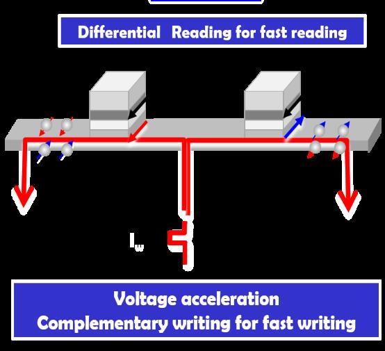
28 VoCSM (Voltage-Control ) Spintronics Memory Non-volatile Memory with Ultra-low Power, High-speed, and Unlimited Endurance Ultra-low Power writing MRAM Dev. Day 2018 Unlimited endurance Patent Japanese patent P , USP 9,881,660: High-density VoCSM (writing 8data with 2 write-pulses) Japanese patent P : High-Speed VoCSM (Complementary writing) Other 21 patents registered and other 27 patents pending Publication Digests of 62nd IEDM, session 27.6, San Francisco, CA, 3 7, December, 2016 Proceedings of IMW 2017, p. 165, Monterey, CA, May, 2017 IEEE Transactions on Magnetics, vol. 53, p , 2017 More than 10 invited talks and other 20 conference talks.
29 New Approaches to Reducing Energy Consumption of MRAM write cycles, Ultra-high efficient (Voltage-Control) Spintronics Memory (VoCSM) H. Yoda Corporate Research & Development Center, Toshiba Corporation Supported by The ImPACT Program of the Council for Science, Technology and Innovation (Cabinet Office, Government of Japan).
30 Summary 1. VoCSM writing is very powful to reduce the writing current to the order of spintronics limitation. 2. High-speed writing and unlimited endurance seem to co-exist for VoCSM. 3. The historical dilemma might be solved. 4. High-speed & high-density architectures were proposed and demonstrated the unique writing schemes. 5. Logic application was introduced and for the long run, it may find applications
31 How to select the bit to write MRAM Dev. Day 2018 unselected bits Selected bits unselected bits V da V a V da 0 Esw VCMA Esw

32 The issues 20nm (i) Static interaction (ii) Resonance Interactions between neighbor bits are big problems Definitely needs to make stray-field small, Like using Ferrimagnets,,
33 V a Write Error Rate Curves I w + 1E+0 1E-1 Conventional spin-hall writing WER 1E-2 1E-3 1E-4 1E-5 VoCSM writing J W (MA/cm 2 ) Deterministic
 ΔEr ~44k B T(80nm 80nm) ΔEr")

34 In-plane MTJ ( aspect ratio of =1 ) ΔEr ~44k B T(80nm 80nm) ΔEr improved by thikker film (1.5nm 2.5nm) MTJ SHE-EL SIL Under layer
Lecture 6 NEW TYPES OF MEMORY
 Lecture 6 NEW TYPES OF MEMORY Memory Logic needs memory to function (efficiently) Current memories Volatile memory SRAM DRAM Non-volatile memory (Flash) Emerging memories Phase-change memory STT-MRAM (Ferroelectric
Perpendicular MTJ stack development for STT MRAM on Endura PVD platform
 Perpendicular MTJ stack development for STT MRAM on Endura PVD platform Mahendra Pakala, Silicon Systems Group, AMAT Dec 16 th, 2014 AVS 2014 *All data in presentation is internal Applied generated data
Page 1. A portion of this study was supported by NEDO.
 MRAM : Materials and Devices Current-induced Domain Wall Motion High-speed MRAM N. Ishiwata NEC Corporation Page 1 A portion of this study was supported by NEDO. Outline Introduction Positioning and direction
From Spin Torque Random Access Memory to Spintronic Memristor. Xiaobin Wang Seagate Technology
 From Spin Torque Random Access Memory to Spintronic Memristor Xiaobin Wang Seagate Technology Contents Spin Torque Random Access Memory: dynamics characterization, device scale down challenges and opportunities
Embedded MRAM Technology For logic VLSI Application
 2011 11th Non-Volatile Memory Technology Symposium Embedded MRAM Technology For logic VLSI Application November 7, 2011 Naoki Kasai 1, Shoji Ikeda 1,2, Takahiro Hanyu 1,3, Tetsuo Endoh 1,4, and Hideo Ohno
NEM Relay Design for Compact, Ultra-Low-Power Digital Logic Circuits
 NEM Relay Design for Compact, Ultra-Low-Power Digital Logic Circuits T.-J. K. Liu 1, N. Xu 1, I.-R. Chen 1, C. Qian 1, J. Fujiki 2 1 Dept. of Electrical Engineering and Computer Sciences University of
Nonvolatile CMOS Circuits Using Magnetic Tunnel Junction
 November 3-4, 2011 Berkeley, CA, USA Nonvolatile CMOS Circuits Using Magnetic Tunnel Junction Hideo Ohno 1,2 1 Center for Spintronics Integrated Systems, Tohoku University, Japan 2 Laboratory for Nanoelectronics
Low-power non-volatile spintronic memory: STT-RAM and beyond
 IOP PUBLISHING JOURNAL OF PHYSICS D: APPLIED PHYSICS J. Phys. D: Appl. Phys. 46 (2013) 074003 (10pp) doi:10.1088/0022-3727/46/7/074003 Low-power non-volatile spintronic memory: STT-RAM and beyond K L Wang,
MTJ-Based Nonvolatile Logic-in-Memory Architecture and Its Application
 2011 11th Non-Volatile Memory Technology Symposium @ Shanghai, China, Nov. 9, 20112 MTJ-Based Nonvolatile Logic-in-Memory Architecture and Its Application Takahiro Hanyu 1,3, S. Matsunaga 1, D. Suzuki
A Universal Memory Model for Design Exploration. Ketul Sutaria, Chi-Chao Wang, Yu (Kevin) Cao School of ECEE, ASU
 Cao School of ECEE, ASU") A Universal Memory Model for Design Exploration Ketul Sutaria, Chi-Chao Wang, Yu (Kevin) Cao School of ECEE, ASU Universal Memory Modeling because there is no universal memory device! Modeling needs in
A Universal Memory Model for Design Exploration Ketul Sutaria, Chi-Chao Wang, Yu (Kevin) Cao School of ECEE, ASU Universal Memory Modeling because there is no universal memory device! Modeling needs in
Wouldn t it be great if
 IDEMA DISKCON Asia-Pacific 2009 Spin Torque MRAM with Perpendicular Magnetisation: A Scalable Path for Ultra-high Density Non-volatile Memory Dr. Randall Law Data Storage Institute Agency for Science Technology
An Overview of Spin-based Integrated Circuits
 ASP-DAC 2014 An Overview of Spin-based Integrated Circuits Wang Kang, Weisheng Zhao, Zhaohao Wang, Jacques-Olivier Klein, Yue Zhang, Djaafar Chabi, Youguang Zhang, Dafiné Ravelosona, and Claude Chappert
MSE 7025 Magnetic Materials (and Spintronics)
") MSE 7025 Magnetic Materials (and Spintronics) Lecture 14: Spin Transfer Torque And the future of spintronics research Chi-Feng Pai cfpai@ntu.edu.tw Course Outline Time Table Week Date Lecture 1 Feb 24
MSE 7025 Magnetic Materials (and Spintronics) Lecture 14: Spin Transfer Torque And the future of spintronics research Chi-Feng Pai cfpai@ntu.edu.tw Course Outline Time Table Week Date Lecture 1 Feb 24
MRAM: Device Basics and Emerging Technologies
 MRAM: Device Basics and Emerging Technologies Matthew R. Pufall National Institute of Standards and Technology 325 Broadway, Boulder CO 80305-3337 Phone: +1-303-497-5206 FAX: +1-303-497-7364 E-mail: pufall@boulder.nist.gov
Author : Fabrice BERNARD-GRANGER September 18 th, 2014
 Author : September 18 th, 2014 Spintronic Introduction Spintronic Design Flow and Compact Modelling Process Variation and Design Impact Semiconductor Devices Characterisation Seminar 2 Spintronic Introduction
Magnetic Tunnel Junction for Integrated Circuits: Scaling and Beyond
 TUTORIAL: APPLIED RESEARCH IN MAGNETISM Magnetic Tunnel Junction for Integrated Circuits: Scaling and Beyond Hideo Ohno 1,2 1 Center for Spintronics Integrated Systems, Tohoku University, Japan 2 Laboratory
A Technology-Agnostic MTJ SPICE Model with User-Defined Dimensions for STT-MRAM Scalability Studies
 A Technology-Agnostic MTJ SPICE Model with User-Defined Dimensions for STT-MRAM Scalability Studies Model download website: mtj.umn.edu Jongyeon Kim 1, An Chen 2, Behtash Behin-Aein 2, Saurabh Kumar 1,
Magnetic tunnel junction beyond memory from logic to neuromorphic computing WANJUN PARK DEPT. OF ELECTRONIC ENGINEERING, HANYANG UNIVERSITY
 Magnetic tunnel junction beyond memory from logic to neuromorphic computing WANJUN PARK DEPT. OF ELECTRONIC ENGINEERING, HANYANG UNIVERSITY Magnetic Tunnel Junctions (MTJs) Structure High density memory
NONVOLATILE SPINTRONICS: PERSPECTIVES ON INSTANT-ON NONVOLATILE NANOELECTRONIC SYSTEMS
 SPIN Vol. 2, No. 2 (2012) 1250009 (22 pages) World Scienti c Publishing Company DOI: 10.1142/S2010324712500099 NONVOLATILE SPINTRONICS: PERSPECTIVES ON INSTANT-ON NONVOLATILE NANOELECTRONIC SYSTEMS K.
MSE 7025 Magnetic Materials (and Spintronics)
") MSE 7025 Magnetic Materials (and Spintronics) Lecture 1: Introduction Chi-Feng Pai cfpai@ntu.edu.tw Course Outline Magnetism and Magnetic Materials What is magnetism? What is its origin? Magnetic properties
MSE 7025 Magnetic Materials (and Spintronics) Lecture 1: Introduction Chi-Feng Pai cfpai@ntu.edu.tw Course Outline Magnetism and Magnetic Materials What is magnetism? What is its origin? Magnetic properties
Center for Spintronic Materials, Interfaces, and Novel Architectures. Voltage Controlled Antiferromagnetics and Future Spin Memory
 Center for Spintronic Materials, Interfaces, and Novel Architectures Voltage Controlled Antiferromagnetics and Future Spin Memory Maxim Tsoi The University of Texas at Austin Acknowledgments: H. Seinige,
Nanoelectronics 12. Atsufumi Hirohata Department of Electronics. Quick Review over the Last Lecture
 Nanoelectronics 12 Atsufumi Hirohata Department of Electronics 09:00 Tuesday, 20/February/2018 (P/T 005) Quick Review over the Last Lecture Origin of magnetism : ( Circular current ) is equivalent to a
A Perpendicular Spin Torque Switching based MRAM for the 28 nm Technology Node
 A Perpendicular Spin Torque Switching based MRAM for the 28 nm Technology Node U.K. Klostermann 1, M. Angerbauer 1, U. Grüning 1, F. Kreupl 1, M. Rührig 2, F. Dahmani 3, M. Kund 1, G. Müller 1 1 Qimonda
Introduction to magnetic recording + recording materials
 Introduction to magnetic recording + recording materials Laurent Ranno Institut Néel, Nanoscience Dept, CNRS-UJF, Grenoble, France I will give two lectures about magnetic recording. In the first one, I
Enhanced spin orbit torques by oxygen incorporation in tungsten films
 Enhanced spin orbit torques by oxygen incorporation in tungsten films Timothy Phung IBM Almaden Research Center, San Jose, California, USA 1 Motivation: Memory devices based on spin currents Spin Transfer
Thursday, July 20 7:30-8:10 Breakfast 8:10-8:30 Welcome and Introduction. Morning Session: The Path Towards MRAM Session Chair: Bob McMichael
 Thursday, July 20 7:30-8:10 Breakfast 8:10-8:30 Welcome and Introduction Morning Session: The Path Towards MRAM Session Chair: Bob McMichael v 8:30-9:15 MRAM Technologies and Metrologies: Present State
Ultralow-Power Reconfigurable Computing with Complementary Nano-Electromechanical Carbon Nanotube Switches
 Ultralow-Power Reconfigurable Computing with Complementary Nano-Electromechanical Carbon Nanotube Switches Presenter: Tulika Mitra Swarup Bhunia, Massood Tabib-Azar, and Daniel Saab Electrical Eng. And
Magnetic Tunnel Junction for Integrated Circuits: Scaling and Beyond
 TUTORIAL: APPLIED RESEARCH IN MAGNETISM Magnetic Tunnel Junction for Integrated Circuits: Scaling and Beyond Hideo Ohno 1,2 1 Center for Spintronics Integrated Systems, Tohoku University, Japan 2 Laboratory
SPICE Modeling of STT-RAM for Resilient Design. Zihan Xu, Ketul Sutaria, Chengen Yang, Chaitali Chakrabarti, Yu (Kevin) Cao School of ECEE, ASU
 Cao School of ECEE, ASU") SPICE odeling of STT-RA for Resilient Design Zihan Xu, Ketul Sutaria, Chengen Yang, Chaitali Chakrabarti, Yu (Kevin) Cao School of ECEE, ASU OUTLINE - 2 - Heterogeneous emory Design A Promising Candidate:
SPICE odeling of STT-RA for Resilient Design Zihan Xu, Ketul Sutaria, Chengen Yang, Chaitali Chakrabarti, Yu (Kevin) Cao School of ECEE, ASU OUTLINE - 2 - Heterogeneous emory Design A Promising Candidate:
Nomenclature, Advantages, Applications. Logic States, Read Ops, Write Ops
 Critical Factors in Testing MRAM Devices W. Stevenson Cypress Semiconductor, Inc Inc. Southwest Test Workshop June G. Asmerom C. Taylor Electroglas AGENDA / OBJECTIVE MRAM Device? Nomenclature, Advantages,
NEUROMORPHIC COMPUTING WITH MAGNETO-METALLIC NEURONS & SYNAPSES: PROSPECTS AND PERSPECTIVES
 NEUROMORPHIC COMPUTING WITH MAGNETO-METALLIC NEURONS & SYNAPSES: PROSPECTS AND PERSPECTIVES KAUSHIK ROY ABHRONIL SENGUPTA, KARTHIK YOGENDRA, DELIANG FAN, SYED SARWAR, PRIYA PANDA, GOPAL SRINIVASAN, JASON
A 68 Parallel Row Access Neuromorphic Core with 22K Multi-Level Synapses Based on Logic- Compatible Embedded Flash Memory Technology
 A 68 Parallel Row Access Neuromorphic Core with 22K Multi-Level Synapses Based on Logic- Compatible Embedded Flash Memory Technology M. Kim 1, J. Kim 1, G. Park 1, L. Everson 1, H. Kim 1, S. Song 1,2,
Access from the University of Nottingham repository:
 ElHassan, Nemat Hassan Ahmed (2017) Development of phase change memory cell electrical circuit model for non-volatile multistate memory device. PhD thesis, University of Nottingham. Access from the University
Two-terminal spin orbit torque magnetoresistive random access memory
 Two-terminal spin orbit torque magnetoresistive random access memory Noriyuki Sato 1, Fen Xue 1,3, Robert M. White 1,2, Chong Bi 1, and Shan X. Wang 1,2,* 1 Stanford University, Department of Electrical
Supplementary Information for. Non-volatile memory based on ferroelectric photovoltaic effect
 Supplementary Information for Non-volatile memory based on ferroelectric photovoltaic effect Rui Guo 1, Lu You 1, Yang Zhou 1, Zhi Shiuh Lim 1, Xi Zou 1, Lang Chen 1, R. Ramesh 2, Junling Wang 1* 1 School
Solid-State Electronics
 Solid-State Electronics 84 (2013) 191 197 Contents lists available at SciVerse ScienceDirect Solid-State Electronics journal homepage: www.elsevier.com/locate/sse Implication logic gates using spin-transfer-torque-operated
Introduction. Simulation methodology. Simulation results
 Introduction Simulation methodology Simulation results Conclusion and Perspectives Introduction Simulation methodology Simulation results Conclusion and Perspectives Radiation induced particles Solar Flare
Moores Law for DRAM. 2x increase in capacity every 18 months 2006: 4GB
 MEMORY Moores Law for DRAM 2x increase in capacity every 18 months 2006: 4GB Corollary to Moores Law Cost / chip ~ constant (packaging) Cost / bit = 2X reduction / 18 months Current (2008) ~ 1 micro-cent
INCREASING power density and static leakage currents
 IEEE TRANSACTIONS ON MAGNETICS, VOL. 51, NO. 5, MAY 2015 3400408 Straintronics-Based Random Access Memory as Universal Data Storage Devices Mahmood Barangi and Pinaki Mazumder, Fellow, IEEE Department
Magnetic Race- Track Memory: Current Induced Domain Wall Motion!
 Magnetic Race- Track Memory: Current Induced Domain Wall Motion! Stuart Parkin IBM Fellow IBM Almaden Research Center San Jose, California parkin@almaden.ibm.com Digital data storage Two main types of
Thin Film Transistors (TFT)
") Thin Film Transistors (TFT) a-si TFT - α-si:h (Hydrogenated amorphous Si) deposited with a PECVD system (low temp. process) replaces the single crystal Si substrate. - Inverted staggered structure with
Thin Film Transistors (TFT) a-si TFT - α-si:h (Hydrogenated amorphous Si) deposited with a PECVD system (low temp. process) replaces the single crystal Si substrate. - Inverted staggered structure with
This document is an author-formatted work. The definitive version for citation appears as:
 This document is an author-formatted work. The definitive version for citation appears as: A. Roohi, R. Zand, D. Fan and R. F. DeMara, "Voltage-based Concatenatable Full Adder using Spin Hall Effect Switching,"
Spin orbit torque driven magnetic switching and memory. Debanjan Bhowmik
 Spin orbit torque driven magnetic switching and memory Debanjan Bhowmik Spin Transfer Torque Fixed Layer Free Layer Fixed Layer Free Layer Current coming out of the fixed layer (F2) is spin polarized in
Thermal Magnetic Random Access Memory
 Thermal Magnetic andom Access Memory IEEE International Conference on Computer Design New Memory Technologies San Jose, CA October 4, 2005 James Deak NVE Corporation Participants Jim Daughton - PI Art
arxiv: v1 [physics.app-ph] 1 May 2017
![arxiv: v1 [physics.app-ph] 1 May 2017](/thumbs/72/67272250.jpg "arxiv: v1 [physics.app-ph] 1 May 2017") Magnetic Skyrmions for Cache Memory Mei-Chin Chen 1 and Kaushik Roy 1 1 School of Electrical and Computer Engineering, Purdue University, West Lafayette, 47906, USA * chen1320@purdue.edu ABSTRACT arxiv:1705.01095v1
Magnetic Skyrmions for Cache Memory Mei-Chin Chen 1 and Kaushik Roy 1 1 School of Electrical and Computer Engineering, Purdue University, West Lafayette, 47906, USA * chen1320@purdue.edu ABSTRACT arxiv:1705.01095v1
Time resolved transport studies of magnetization reversal in orthogonal spin transfer magnetic tunnel junction devices
 Invited Paper Time resolved transport studies of magnetization reversal in orthogonal spin transfer magnetic tunnel junction devices Georg Wolf a, Gabriel Chaves-O Flynn a, Andrew D. Kent a, Bartek Kardasz
Magnetic core memory (1951) cm 2 ( bit)
 cm 2 ( bit)") Magnetic core memory (1951) 16 16 cm 2 (128 128 bit) Semiconductor Memory Classification Read-Write Memory Non-Volatile Read-Write Memory Read-Only Memory Random Access Non-Random Access EPROM E 2 PROM
Magnetic core memory (1951) 16 16 cm 2 (128 128 bit) Semiconductor Memory Classification Read-Write Memory Non-Volatile Read-Write Memory Read-Only Memory Random Access Non-Random Access EPROM E 2 PROM
S. Mangin 1, Y. Henry 2, D. Ravelosona 3, J.A. Katine 4, and S. Moyerman 5, I. Tudosa 5, E. E. Fullerton 5
 Spin transfer torques in high anisotropy magnetic nanostructures S. Mangin 1, Y. enry 2, D. Ravelosona 3, J.A. Katine 4, and S. Moyerman 5, I. Tudosa 5, E. E. Fullerton 5 1) Laboratoire de Physique des
Mechanism of Switching and Related Challenges in Transition Metal Oxide Based RRAM Devices
 Mechanism of Switching and Related Challenges in Transition Metal Oxide Based RRAM Devices Rashmi Jha and Branden Long Dept. of Electrical Engineering and Computer Science University of Toledo Toledo,
Improving STT-MRAM Density Through Multibit Error Correction
 Improving STT-MRAM Density Through Multibit Error Correction Brandon Del Bel, Jongyeon Kim, Chris H. Kim, and Sachin S. Sapatnekar Department of ECE, University of Minnesota {delbel, kimx2889, chriskim,
Name: Answers. Mean: 83, Standard Deviation: 12 Q1 Q2 Q3 Q4 Q5 Q6 Total. ESE370 Fall 2015
 University of Pennsylvania Department of Electrical and System Engineering Circuit-Level Modeling, Design, and Optimization for Digital Systems ESE370, Fall 2015 Final Tuesday, December 15 Problem weightings
V High frequency magnetic measurements
 V High frequency magnetic measurements Rémy Lassalle-Balier What we are doing and why Ferromagnetic resonance CHIMP memory Time-resolved magneto-optic Kerr effect NISE Task 8 New materials Spin dynamics
LH5P832. CMOS 256K (32K 8) Pseudo-Static RAM
 Pseudo-Static RAM") LH5P832 CMOS 256K (32K 8) Pseudo-Static RAM FEATURES 32,768 8 bit organization Access time: 100/120 ns (MAX.) Cycle time: 160/190 ns (MIN.) Power consumption: Operating: 357.5/303 mw Standby: 16.5 mw TTL
LH5P832 CMOS 256K (32K 8) Pseudo-Static RAM FEATURES 32,768 8 bit organization Access time: 100/120 ns (MAX.) Cycle time: 160/190 ns (MIN.) Power consumption: Operating: 357.5/303 mw Standby: 16.5 mw TTL
Giant Magnetoresistance
 Giant Magnetoresistance 03/18/2010 Instructor: Dr. Elbio R. Dagotto Class: Solid State Physics 2 Nozomi Shirato Department of Materials Science and Engineering ntents: Giant Magnetoresistance (GMR) Discovery
Introduction to Computer Engineering. CS/ECE 252, Fall 2012 Prof. Guri Sohi Computer Sciences Department University of Wisconsin Madison
 Introduction to Computer Engineering CS/ECE 252, Fall 2012 Prof. Guri Sohi Computer Sciences Department University of Wisconsin Madison Chapter 3 Digital Logic Structures Slides based on set prepared by
Advanced Topics In Solid State Devices EE290B. Will a New Milli-Volt Switch Replace the Transistor for Digital Applications?
 Advanced Topics In Solid State Devices EE290B Will a New Milli-Volt Switch Replace the Transistor for Digital Applications? August 28, 2007 Prof. Eli Yablonovitch Electrical Engineering & Computer Sciences
Chapter 7. Sequential Circuits Registers, Counters, RAM
 Chapter 7. Sequential Circuits Registers, Counters, RAM Register - a group of binary storage elements suitable for holding binary info A group of FFs constitutes a register Commonly used as temporary storage
GMU, ECE 680 Physical VLSI Design 1
 ECE680: Physical VLSI Design Chapter VIII Semiconductor Memory (chapter 12 in textbook) 1 Chapter Overview Memory Classification Memory Architectures The Memory Core Periphery Reliability Case Studies
Gate voltage modulation of spin-hall-torque-driven magnetic switching. Cornell University, Ithaca, NY 14853
 Gate voltage modulation of spin-hall-torque-driven magnetic switching Luqiao Liu 1, Chi-Feng Pai 1, D. C. Ralph 1,2 and R. A. Buhrman 1 1 Cornell University, Ithaca, NY 14853 2 Kavli Institute at Cornell,
Spin Torque and Magnetic Tunnel Junctions
 Spin Torque and Magnetic Tunnel Junctions Ed Myers, Frank Albert, Ilya Krivorotov, Sergey Kiselev, Nathan Emley, Patrick Braganca, Greg Fuchs, Andrei Garcia, Ozhan Ozatay, Eric Ryan, Jack Sankey, John
Digital Integrated Circuits A Design Perspective
 Semiconductor Memories Adapted from Chapter 12 of Digital Integrated Circuits A Design Perspective Jan M. Rabaey et al. Copyright 2003 Prentice Hall/Pearson Outline Memory Classification Memory Architectures
LH5P8128. CMOS 1M (128K 8) Pseudo-Static RAM PIN CONNECTIONS
 Pseudo-Static RAM PIN CONNECTIONS") LH5P8128 FEATURES 131,072 8 bit organization Access times (MAX.): 60/80/100 ns Cycle times (MIN.): 100/130/160 ns Single +5 V power supply Power consumption: Operating: 572/385/275 mw (MAX.) Standby (CMOS
LH5P8128 FEATURES 131,072 8 bit organization Access times (MAX.): 60/80/100 ns Cycle times (MIN.): 100/130/160 ns Single +5 V power supply Power consumption: Operating: 572/385/275 mw (MAX.) Standby (CMOS
Memory Trend. Memory Architectures The Memory Core Periphery
 Semiconductor Memories: an Introduction ti Talk Overview Memory Trend Memory Classification Memory Architectures The Memory Core Periphery Reliability Semiconductor Memory Trends (up to the 90 s) Memory
CMOS Digital Integrated Circuits Lec 13 Semiconductor Memories
 Lec 13 Semiconductor Memories 1 Semiconductor Memory Types Semiconductor Memories Read/Write (R/W) Memory or Random Access Memory (RAM) Read-Only Memory (ROM) Dynamic RAM (DRAM) Static RAM (SRAM) 1. Mask
Emerging Memory Technologies
 Emerging Memory Technologies Minal Dubewar 1, Nibha Desai 2, Subha Subramaniam 3 1 Shah and Anchor kutchhi college of engineering, 2 Shah and Anchor kutchhi college of engineering, 3 Shah and Anchor kutchhi
Kaushik Roy Department of Electrical and Computer Engineering, Purdue University, West Lafayette, IN https://engineering.purdue.edu/nrl/index.
 Beyond Charge-Based Computing: STT- MRAMs Kaushik Roy Department of Electrical and Computer Engineering, Purdue University, West Lafayette, IN https://engineering.purdue.edu/nrl/index.html 1 Failure probability
Electrical and Reliability Characteristics of RRAM for Cross-point Memory Applications. Hyunsang Hwang
 Electrical and Reliability Characteristics of RRAM for Cross-point Memory Applications Hyunsang Hwang Dept. of Materials Science and Engineering Gwangju Institute of Science and Technology (GIST), KOREA
IEEE JOURNAL ON EXPLORATORY SOLID-STATE COMPUTATIONAL DEVICES AND CIRCUITS 1
 IEEE JOURNAL ON EXPLORATORY SOLID-STATE COMPUTATIONAL DEVICES AND CIRCUITS 1 A Comparative Study between Spin-Transfer-Torque (STT) and Spin-Hall-Effect (SHE) Switching Mechanisms in PMTJ using SPICE Ibrahim
Magnetization Dynamics in Spintronic Structures and Devices
 Japanese Journal of Applied Physics Vol. 45, No. 5A, 2006, pp. 3835 3841 #2006 The Japan Society of Applied Physics Magnetization Dynamics in Spintronic Structures and Devices Structure, Materials and
Center for Spintronic Materials, Interfaces, and Novel Architectures. Spintronics Enabled Efficient Neuromorphic Computing: Prospects and Perspectives
 Center for Spintronic Materials, Interfaces, and Novel Architectures Spintronics Enabled Efficient Neuromorphic Computing: Prospects and Perspectives KAUSHIK ROY ABHRONIL SENGUPTA, KARTHIK YOGENDRA, DELIANG
Creating non-volatile electronics by spintronics technology
 Research paper Creating non-volatile electronics by spintronics technology - Toward developing ultimate green IT devices - Shinji Yuasa *, Hitoshi Kubota, Akio Fukushima, Kay Yakushiji, Taro Nagahama,
Index. annealing temperature 236, 238, 250, 310, , , 491, 691
 Index Abbe s diffraction limit 42 absorption coefficient 96 97, 107 108, 128 access device 436, 599, 604, 607, 615 access transistor 435 437, 592 593, 596, 603, 606 activation energy 215, 296 297, 411,
SEMICONDUCTOR MEMORIES
 SEMICONDUCTOR MEMORIES Semiconductor Memory Classification RWM NVRWM ROM Random Access Non-Random Access EPROM E 2 PROM Mask-Programmed Programmable (PROM) SRAM FIFO FLASH DRAM LIFO Shift Register CAM
Single Spin Qubits, Qubit Gates and Qubit Transfer with Quantum Dots
 International School of Physics "Enrico Fermi : Quantum Spintronics and Related Phenomena June 22-23, 2012 Varenna, Italy Single Spin Qubits, Qubit Gates and Qubit Transfer with Quantum Dots Seigo Tarucha
Recent developments in spintronic
 Recent developments in spintronic Tomas Jungwirth nstitute of Physics ASCR, Prague University of Nottingham in collaboration with Hitachi Cambridge, University of Texas, Texas A&M University - Spintronics
New Ferroelectric Material for Embedded FRAM LSIs
 New Ferroelectric Material for Embedded FRAM LSIs V Kenji Maruyama V Masao Kondo V Sushil K. Singh V Hiroshi Ishiwara (Manuscript received April 5, 2007) The strong growth of information network infrastructures
Semiconductor Memories
 !"#"$%&'()$*#+%$*,' -"+./"$0 1'!*0"#)'2*+03*.$"4* Jan M. Rabaey Anantha Chandrakasan Borivoje Nikolic Semiconductor Memories December 20, 2002 !"#$%&'()*&'*+&, Memory Classification Memory Architectures
Developing IoT-Based Factory Automation Using F-RAM
 Developing IoT-Based Factory Automation Using F-RAM Douglas Mitchell Flash Memory Summit 2018 Santa Clara, CA 1 INDUSTRIAL SYSTEMS TODAY Industry 4.0 The smart factory, Cyber-physical systems monitor factory
9. Spin Torque Majority Gate
 eyond MOS computing 9. Spin Torque Majority Gate Dmitri Nikonov Thanks to George ourianoff Dmitri.e.nikonov@intel.com 1 Outline Spin majority gate with in-pane magnetization Spin majority gate with perpendicular
Spin-orbit torque magnetization switching of a three-terminal. perpendicular magnetic tunnel junction
 Spin-orbit torque magnetization switching of a three-terminal perpendicular magnetic tunnel junction Murat Cubukcu 1, Olivier Boulle 1, Marc Drouard 1, Kevin Garello 2, Can Onur Avci 2, Ioan Mihai Miron
Electric-Field-Controlled Magnetoelectric RAM: Progress, Challenges, and Scaling
 IEEE TRANSACTIONS ON MAGNETICS, VOL. 51, NO. 11, NOVEMBER 2015 3401507 Electric-Field-Controlled Magnetoelectric RAM: Progress, Challenges, and Scaling Pedram Khalili Amiri 1,2,JuanG.Alzate 1, Xue Qing
Advanced Spintronic Memory and Logic For Non-Volatile Processors
 Advanced Spintronic Memory and Logic For Non-Volatile Processors Robert Perricone, Ibrahim Ahmed, Zhaoxin Liang, Meghna G. Mankalale, X. Sharon Hu, Chris H. Kim, Michael Niemier, Sachin S. Sapatnekar,
Modelling and Circuit Design for STT-MRAM. Aynaz Vatankhahghadim
 Modelling and Circuit Design for STT-MRAM by Aynaz Vatankhahghadim A thesis submitted in conformity with the requirements for the degree of Doctor of Philosophy Graduate Department of Electrical and Computer
Random Access Memory. DRAM & SRAM Design DRAM SRAM MS635. Dynamic Random Access Memory. Static Random Access Memory. Cell Structure. 6 Tr.
 DRAM & SRAM Design Random Access Memory Volatile memory Random access is possible if you know the address DRAM DRAM Dynamic Random Access Memory SRAM Static Random Access Memory SRAM Cell Structure Power
DS K x 8 Static RAM FEATURES PIN ASSIGNMENT PIN DESCRIPTION
 8K x 8 Static RAM FEATURES Low power CMOS design Standby current 50 na max at t A = 25 C V CC = 3.0V 100 na max at t A = 25 C V CC = 5.5V 1 µa max at t A = 60 C V CC = 5.5V Full operation for V CC = 4.5V
DS1225Y. 64K Nonvolatile SRAM FEATURES PIN ASSIGNMENT
 DS1225Y 64K Nonvolatile SRAM FEATURES years minimum data retention in the absence of external power PIN ASSIGNMENT NC 1 28 VCC Data is automatically protected during power loss Directly replaces 8K x 8
Semiconductor Memories
 Semiconductor References: Adapted from: Digital Integrated Circuits: A Design Perspective, J. Rabaey UCB Principles of CMOS VLSI Design: A Systems Perspective, 2nd Ed., N. H. E. Weste and K. Eshraghian
Semiconductor Memories
 Digital Integrated Circuits A Design Perspective Jan M. Rabaey Anantha Chandrakasan Borivoje Nikolic Semiconductor Memories December 20, 2002 Chapter Overview Memory Classification Memory Architectures
ESE 570: Digital Integrated Circuits and VLSI Fundamentals
 ESE 570: Digital Integrated Circuits and VLSI Fundamentals Lec 21: April 4, 2017 Memory Overview, Memory Core Cells Penn ESE 570 Spring 2017 Khanna Today! Memory " Classification " ROM Memories " RAM Memory
74LVC823A 9-bit D-type flip-flop with 5-volt tolerant inputs/outputs; positive-edge trigger (3-State)
") INTEGRATED CIRCUITS inputs/outputs; positive-edge trigger (3-State) 1998 Sep 24 FEATURES 5-volt tolerant inputs/outputs, for interfacing with 5-volt logic Supply voltage range of 2.7V to 3.6V Complies
INTEGRATED CIRCUITS inputs/outputs; positive-edge trigger (3-State) 1998 Sep 24 FEATURES 5-volt tolerant inputs/outputs, for interfacing with 5-volt logic Supply voltage range of 2.7V to 3.6V Complies
Digital Integrated Circuits A Design Perspective. Semiconductor. Memories. Memories
 Digital Integrated Circuits A Design Perspective Semiconductor Chapter Overview Memory Classification Memory Architectures The Memory Core Periphery Reliability Case Studies Semiconductor Memory Classification
Spintronics. Seminar report SUBMITTED TO: SUBMITTED BY:
 A Seminar report On Spintronics Submitted in partial fulfillment of the requirement for the award of degree of Electronics SUBMITTED TO: SUBMITTED BY: www.studymafia.org www.studymafia.org Preface I have
BEYOND CHARGE-BASED COMPUTING: STT-MRAMS
 BEYOND CHARGE-BASED COMPUTING: STT-MRAMS KAUSHIK ROY XUANYAO FONG, CHARLES AUGUSTINE, GEORGE PANAGOPOULOS, YUSUNG KIM, KONWOO KWON, HARSHA CHODAY, MRIGANK SHARAD, ANAND RAGHUNATHAN https://engineering.purdue.edu/nrl/index.html
Field-free switching of perpendicular magnetic tunnel junction by the interplay
 Field-free switching of perpendicular magnetic tunnel junction by the interplay of spin orbit and spin transfer torques Mengxing Wang 1, Wenlong Cai 1, Daoqian Zhu 1, Jimmy Kan 2, Zhengyang Zhao 3, Kaihua
Magnetic memories: from magnetic storage to MRAM and magnetic logic
 Magnetic memories: from magnetic storage to MRAM and magnetic logic WIND Claude CHAPPERT, CNRS Département "Nanospintronique" Institut d'electronique Fondamentale Université Paris Sud, Orsay, FRANCE chappert@u-psud.fr
Compact Modeling of STT-RAM and MeRAM A Verilog-A model of Magnetic Tunnel Junction Behavioral Dynamics
 UNIVERSITY OF CALIFORNIA, LOS ANGELES Compact Modeling of STT-RAM and MeRAM A Verilog-A model of Magnetic Tunnel Junction Behavioral Dynamics Dheeraj Srinivasan 3/8/2013 +This work was done under the advisement
CMPEN 411 VLSI Digital Circuits Spring Lecture 21: Shifters, Decoders, Muxes
 CMPEN 411 VLSI Digital Circuits Spring 2011 Lecture 21: Shifters, Decoders, Muxes [Adapted from Rabaey s Digital Integrated Circuits, Second Edition, 2003 J. Rabaey, A. Chandrakasan, B. Nikolic] Sp11 CMPEN
MAGNETORESISTIVE random access memory
 1 Comparative Evaluation of Spin-Transfer-Torque and Magnetoelectric Random Access Memory Shaodi Wang, Hochul Lee, Farbod Ebrahimi, P. Khalili Amiri, Kang L. Wang, Fellow, IEEE, and Puneet Gupta Department
NV Electronically Programmable Capacitor
 Small Packages MSOP Flipchip NV Electronically Programmable Capacitor FEATURES Non-volatile EEPROM storage of programmed trim codes Power On Recall of capacitance setting High-Performance Electronically
Lecture 25. Semiconductor Memories. Issues in Memory
 Lecture 25 Semiconductor Memories Issues in Memory Memory Classification Memory Architectures TheMemoryCore Periphery 1 Semiconductor Memory Classification RWM NVRWM ROM Random Access Non-Random Access