Low Energy Spin Transfer Torque RAM (STT-RAM / SPRAM) Zach Foresta April 23, 2009
|
|
|
- Russell Sanders
- 6 years ago
- Views:
Transcription


1 Low Energy Spin Transfer Torque RAM (STT-RAM / SPRAM) Zach Foresta April 23, 2009

2 Overview Background A brief history GMR and why it occurs TMR structure What is spin transfer? A novel device A future for SPRAM


3 Background Timeline Events leading to the discovery of Spin Transfer Torque RAM Lord Kelvin observes anisotropic magnetic resistance (AMR) 1857 Sir Neville Mott develops model for the anomalous electrical resistivities of the ferromagnetic transitionmetals 1936 Michel Julliere discovers TMR at very low temperatures 1975 Terunobu Miyazaki discovers room temperature TMR 1995 Slonczewski and Berger propose concept of "spin transfer" 1996 First prototype 2MBit SPRAM device Predicted TMR ratios of 1000% using MgO barrier layer 2001 IBM uses GMR devices in read heads for hard drives Fert and Grünberg discover GMR 1988

4 Background Anisotropic Magneto-resistance (AMR) Lord Kelvin discovers AMR using Fe and Ni I found that iron, when subjected to magnetic force, acquires an increase of resistance to the conduction of electricity across, the lines of magnetization the electric conductivity of nickel is similarly influenced by magnetism, but to a greater degree -Lord Kelvin, Proceedings of the Royal Society of London, Vol. 8, 1857, pp
 The concept for spin transfer")

5 Background Giant Magneto-resistance (GMR) The concept for spin transfer evolved from the physical principles of GMR Fathers of GMR Albert Fert Peter Grünberg
 Pinned Layer- ferromagnetic (FM) Nonmagnetic (NM) Free Layer-")
6 Background Giant Magneto-resistance (GMR) Spin valve type GMR device Anti-ferromagnetic (AF) Pinned Layer- ferromagnetic (FM) Nonmagnetic (NM) Free Layer- ferromagnetic (FM)
7 Background Giant Magneto-resistance (GMR) External magnetic field switches the orientation of the free layer between parallel (P) and anti-parallel (AP) Resistance in the P-state is lower than the AP-state (R AP > R P ) Good at differentiating between 1 or 0 using changes in resistance
 Practical Application IBM HD read")
8 Background Giant Magneto-resistance (GMR) Practical Application IBM HD read heads

9 Background GMR why it occurs? 1922 Stern-Gerlach Experiment Electrons have intrinsic angular momentum which depend on their quantized spin number (m s = ±1/2)
10 Background GMR why it occurs? Electrical Resistance is caused by electron scattering Probability of scattering depends on the number of available quantum states for the electron to scatter into, which depends strongly on the relative direction of the electron's spin and the magnetic field inside the FM layer.

11 Background GMR why it occurs? GMR effect in the P and AP states P-state experiences less scattering Up spin electrons have no states to scatter into.
12 Background Tunneling Magneto-resistance (TMR) 1975 Discovered by Michel Julliere At 4.2 K Julliere observed resistance changes on the order of 14% His work was disregarded as impractical until room temperature TMR was achieved in 1995 by Terunobu Miyazaki
13 Background TMR structure SPRAM devices implements a TMR structure Main differences between TMR and GMR GMR has a middle NM layer whereas TMR uses an insulator TMR uses current induced magnetic fields to switch from AP to P states and vice versa TMR achieves resistance ratio results on the order 500% (GMR ~ 50%) Today s HD readers are predominantly using TMR structures

14 Background TMR structure Cobalt ferromagnetic layers Magnesium Oxide insulating barrier layer

15 Background TMR structure Why Co? Cobalt is missing 3 electron in the 3d level Sir Neville Mott s model states that the 3d level electrons act as scatterers near the fermi level. The density of states at the fermi energy is mostly spin down meaning Co has more quantum states for scattering.

16 Background TMR structure Why MgO? Magnesium oxide has a cubic crystalline structure which aids in conservation of electron momentum transfer 2001 predicted TMR ratio of 1000% using this insulating layer.
17 What is Spin Transfer? 1996 Slonczewski and Berger propose the idea of spin transfer When a current of polarized electrons enters a ferro-magnet, there is generally a transfer of angular momentum between propagating electrons and the magnetization of the film.

18 What is Spin Transfer? In short instead of changing the magnetic field externally it is done by polarized currents. The result Similar to GMR/TMR a resistance change is seen from AP to P states.
/")
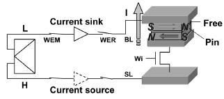
19 A Novel Device A group developed a 1.8 V 2Mb SPRAM chip Using NiFe(2nm)/ CoFe(1nm)/MgO(1nm)/CoFe(1nm) TMR memory cell
 where state is read Source")

20 A Novel Device Components of one Bit Bit Line (BL) where state is read Source Line (SL) current source Word Line (WL) current state regulator TMR device memory cell

21 A Novel Device Writing 0 s and 1 s
22 Novel Device Major Pitfalls Switching Current Direction In order to write 0 or 1 current must be either into or out of SL Reading Bits without accidental writing Reading is similar to writing There exists a critical current density Jc - for parallelizing and Jc + for anti-parallelizing.
23 Novel Device Current Switching Use a flip flop gate depending on inputs of SALT and SALB Example SALT = High (H) + SALB = Low (L) = parallelizing (BL to SL)

24 Novel Device Parallelizing Anti-Parallelizing
25 Novel Device Accidental writing while reading (accidental spin reversal) Disturbance a measure of likelihood of spin reversal. Parallelizing direction has larger disturbance when reading AP-state, therefore lower chance of spin reversal.
26 Novel Device Testing this hypothesis by varying the TMR ratio For P direction As TMR ratio increases the possibility of spin reversal decreases. For AP direction does not depend on TMR ratio.

27 Novel Device Finished Product
28 Novel Device Proven 10 year life cycle No degradation of R AP / R P after 1 billion write cycles Fast read/write Non-volatile Instant-ON capable Low energy

29 Future of SPRAM How it compares against MRAM Scalability > MRAM Lower Energy More complex control scheme
30 Future of SPRAM Potential for higher speeds Research conducted by Sarah Gerretsen, University of California TMR device of Co (20nm) /MgO (5nm) /Co (5nm) with a switching current of 1.96mA resulted in a 0.104ns P to AP state switching time
; Interaction of electrons with spinwaves in the bulk and in multilayers cond-mat /0203314. 3. M.D. Stiles & A. Zangwill. Anatomy of Spin-Transfer Torque. May 2002 4.")
31 Work Cited 1. J. C. Slonczewski, J. Magn. Magn. Mater. 159, L1 (1996); 195, L261 (1999). 2. L. Berger, Phys. Rev. B 54, 9353 (1996); J. Appl. Phys. 81, 4880 (1997); Phys. Rev. B 59, (1999); J. Appl. Phys. 89, 5521 (2001); Interaction of electrons with spinwaves in the bulk and in multilayers cond-mat / M.D. Stiles & A. Zangwill. Anatomy of Spin-Transfer Torque. May Alain Schuhl, Daniel Lacour, C. R. Physique 6 (2005) P. M. Levy An Idiosyncratic History of Giant Magnetoresistance. NSDL Classic Articles in Context. Issue 2, December < wiki.nsdl.org/index.php/pale:classicarticles/gmr> 6. Butler, W.H., Zhang, X.G., Schulthess, T.C. & MacLaren, J.M., Spin-dependent Tunneling Conductance of Fe MgO Fe Sandwiches. Phys. Rev. B 63, and Mathon, J. & A. Umerski, A., Theory of Tunneling Magnetoresistance of an Epitaxial Fe/MgO/Fe(001) Junction. Phys. Rev. 63, (R) 7. S. Maekawa & T. Shinjo. Spin Dependent Transport in Magnetic Nanostructures. (Eds.) London: Taylor and Francis (2002) pg Kawahara, T., Takemura, R., Miura, K., Hayakawa, J., Ikeda, S., Lee, Y.M., Sasaki, R., Goto,Y., Ito,K., Meguro, T., Matsukura, F., Takahashi, H., Matsuoka, H. & Ohno, H.. 2 Mb SPRAM (SPin-Transfer Torque RAM) With Bit-by-Bit Bi-Directional Current Write and Parallelizing-Direction Current Read. IEEE Journal of Solid-State Circuits, vol. 43, NO. 1, January 2008 pg Sarah Gerretsen. Spin Transfer Torque in Ferromagnetic Materials. Department of Physics and Astronomy, University of California, Los Angles, Ca, J. C. Sankey, Y.-T. Cui, R. A. Buhrman, D. C. Ralph, J. Z. Sun, J. C. Slonczewski. Measurement of the Spin-Transfer- Torque Vector in Magnetic Tunnel Junctions. Nature Physics 4, (2008) 11. V. K. Dugaev, J. Barnas. Classical description of current-induced spin-transfer torque in multilayer structures. J. Appl. Phys. 97, (2005) 12. Evgeny Y. Tsymbal. "Magnetic Tunnel Junction." < physics.unl.edu/~tsymbal/tsymbal_files/tmr/sdt_files/page0001.html>.
32 Questions
Low Energy SPRAM. Figure 1 Spin valve GMR device hysteresis curve showing states of parallel (P)/anti-parallel (AP) poles,
/anti-parallel (AP) poles,") Zachary Foresta Nanoscale Electronics 04-22-2009 Low Energy SPRAM Introduction The concept of spin transfer was proposed by Slonczewski [1] and Berger [2] in 1996. They stated that when a current of polarized
Zachary Foresta Nanoscale Electronics 04-22-2009 Low Energy SPRAM Introduction The concept of spin transfer was proposed by Slonczewski [1] and Berger [2] in 1996. They stated that when a current of polarized
From Hall Effect to TMR
 From Hall Effect to TMR 1 Abstract This paper compares the century old Hall effect technology to xmr technologies, specifically TMR (Tunnel Magneto-Resistance) from Crocus Technology. It covers the various
Giant Magnetoresistance
 Giant Magnetoresistance N. Shirato urse: Solid State Physics 2, Spring 2010, Instructor: Dr. Elbio Dagotto Department of Materials Science and Engineering, University of Tennessee, Knoxville, TN 37996
MAGNETORESISTANCE PHENOMENA IN MAGNETIC MATERIALS AND DEVICES. J. M. De Teresa
 MAGNETORESISTANCE PHENOMENA IN MAGNETIC MATERIALS AND DEVICES J. M. De Teresa Instituto de Ciencia de Materiales de Aragón, Universidad de Zaragoza-CSIC, Facultad de Ciencias, 50009 Zaragoza, Spain. E-mail:
Mon., Feb. 04 & Wed., Feb. 06, A few more instructive slides related to GMR and GMR sensors
 Mon., Feb. 04 & Wed., Feb. 06, 2013 A few more instructive slides related to GMR and GMR sensors Oscillating sign of Interlayer Exchange Coupling between two FM films separated by Ruthenium spacers of
Mesoscopic Spintronics
 Mesoscopic Spintronics Taro WAKAMURA (Université Paris-Sud) Lecture 1 Today s Topics 1.1 History of Spintronics 1.2 Fudamentals in Spintronics Spin-dependent transport GMR and TMR effect Spin injection
Ferromagnetism and Electronic Transport. Ordinary magnetoresistance (OMR)
") Ferromagnetism and Electronic Transport There are a number of effects that couple magnetization to electrical resistance. These include: Ordinary magnetoresistance (OMR) Anisotropic magnetoresistance (AMR)
Ferromagnetism and Electronic Transport There are a number of effects that couple magnetization to electrical resistance. These include: Ordinary magnetoresistance (OMR) Anisotropic magnetoresistance (AMR)
Some pictures are taken from the UvA-VU Master Course: Advanced Solid State Physics by Anne de Visser (University of Amsterdam), Solid State Course
, Solid State Course") Some pictures are taken from the UvA-VU Master Course: Advanced Solid State Physics by Anne de Visser (University of Amsterdam), Solid State Course by Mark Jarrel (Cincinnati University), from Ibach and
Some pictures are taken from the UvA-VU Master Course: Advanced Solid State Physics by Anne de Visser (University of Amsterdam), Solid State Course by Mark Jarrel (Cincinnati University), from Ibach and
Advanced Lab Course. Tunneling Magneto Resistance
 Advanced Lab Course Tunneling Magneto Resistance M06 As of: 015-04-01 Aim: Measurement of tunneling magnetoresistance for different sample sizes and recording the TMR in dependency on the voltage. Content
SPINTRONICS. Waltraud Buchenberg. Faculty of Physics Albert-Ludwigs-University Freiburg
 SPINTRONICS Waltraud Buchenberg Faculty of Physics Albert-Ludwigs-University Freiburg July 14, 2010 TABLE OF CONTENTS 1 WHAT IS SPINTRONICS? 2 MAGNETO-RESISTANCE STONER MODEL ANISOTROPIC MAGNETO-RESISTANCE
Lecture 6 NEW TYPES OF MEMORY
 Lecture 6 NEW TYPES OF MEMORY Memory Logic needs memory to function (efficiently) Current memories Volatile memory SRAM DRAM Non-volatile memory (Flash) Emerging memories Phase-change memory STT-MRAM (Ferroelectric
Giant Magnetoresistance
 Giant Magnetoresistance Zachary Barnett Course: Solid State II; Instructor: Elbio Dagotto; Semester: Spring 2008 Physics Department, University of Tennessee (Dated: February 24, 2008) This paper briefly
Current-driven Magnetization Reversal in a Ferromagnetic Semiconductor. (Ga,Mn)As/GaAs/(Ga,Mn)As Tunnel Junction
As/GaAs/(Ga,Mn)As Tunnel Junction") Current-driven Magnetization Reversal in a Ferromagnetic Semiconductor (Ga,Mn)As/GaAs/(Ga,Mn)As Tunnel Junction D. Chiba 1, 2*, Y. Sato 1, T. Kita 2, 1, F. Matsukura 1, 2, and H. Ohno 1, 2 1 Laboratory
Current-driven Magnetization Reversal in a Ferromagnetic Semiconductor (Ga,Mn)As/GaAs/(Ga,Mn)As Tunnel Junction D. Chiba 1, 2*, Y. Sato 1, T. Kita 2, 1, F. Matsukura 1, 2, and H. Ohno 1, 2 1 Laboratory
spin-dependent scattering of electrons in ferromagnetic layers antiferromagnetic interlayer exchange coupling
 industrial impact of the GMR and related spin electronics effects is presented in Section 6. Finally, the Curriculum Vitae of Albert Fert and Peter Grünberg are given in two Appendices. 2. The GMR effect
Giant Magnetoresistance
 Giant Magnetoresistance 03/18/2010 Instructor: Dr. Elbio R. Dagotto Class: Solid State Physics 2 Nozomi Shirato Department of Materials Science and Engineering ntents: Giant Magnetoresistance (GMR) Discovery
NOVEL GIANT MAGNETORESISTANCE MODEL USING MULTIPLE BARRIER POTENTIAL
 NOVEL GIANT MAGNETORESISTANCE MODEL USING MULTIPLE BARRIER POTENTIAL Christian Fredy Naa, Suprijadi, Sparisoma Viridi and Mitra Djamal Department of Physics, Faculty of Mathematics and Natural Science,
MSE 7025 Magnetic Materials (and Spintronics)
") MSE 7025 Magnetic Materials (and Spintronics) Lecture 14: Spin Transfer Torque And the future of spintronics research Chi-Feng Pai cfpai@ntu.edu.tw Course Outline Time Table Week Date Lecture 1 Feb 24
MSE 7025 Magnetic Materials (and Spintronics) Lecture 14: Spin Transfer Torque And the future of spintronics research Chi-Feng Pai cfpai@ntu.edu.tw Course Outline Time Table Week Date Lecture 1 Feb 24
Nanoelectronics 12. Atsufumi Hirohata Department of Electronics. Quick Review over the Last Lecture
 Nanoelectronics 12 Atsufumi Hirohata Department of Electronics 09:00 Tuesday, 20/February/2018 (P/T 005) Quick Review over the Last Lecture Origin of magnetism : ( Circular current ) is equivalent to a
Giant Magnetoresistance
 GENERAL ARTICLE Giant Magnetoresistance Nobel Prize in Physics 2007 Debakanta Samal and P S Anil Kumar The 2007 Nobel Prize in Physics was awarded to Albert Fert and Peter Grünberg for the discovery of
MRAM: Device Basics and Emerging Technologies
 MRAM: Device Basics and Emerging Technologies Matthew R. Pufall National Institute of Standards and Technology 325 Broadway, Boulder CO 80305-3337 Phone: +1-303-497-5206 FAX: +1-303-497-7364 E-mail: pufall@boulder.nist.gov
arxiv: v1 [cond-mat.mtrl-sci] 28 Jul 2008
![arxiv: v1 [cond-mat.mtrl-sci] 28 Jul 2008](/thumbs/88/117898456.jpg "arxiv: v1 [cond-mat.mtrl-sci] 28 Jul 2008") Current induced resistance change of magnetic tunnel junctions with ultra-thin MgO tunnel barriers Patryk Krzysteczko, 1, Xinli Kou, 2 Karsten Rott, 1 Andy Thomas, 1 and Günter Reiss 1 1 Bielefeld University,
Current induced resistance change of magnetic tunnel junctions with ultra-thin MgO tunnel barriers Patryk Krzysteczko, 1, Xinli Kou, 2 Karsten Rott, 1 Andy Thomas, 1 and Günter Reiss 1 1 Bielefeld University,
Wouldn t it be great if
 IDEMA DISKCON Asia-Pacific 2009 Spin Torque MRAM with Perpendicular Magnetisation: A Scalable Path for Ultra-high Density Non-volatile Memory Dr. Randall Law Data Storage Institute Agency for Science Technology
From Spin Torque Random Access Memory to Spintronic Memristor. Xiaobin Wang Seagate Technology
 From Spin Torque Random Access Memory to Spintronic Memristor Xiaobin Wang Seagate Technology Contents Spin Torque Random Access Memory: dynamics characterization, device scale down challenges and opportunities
introduction: what is spin-electronics?
 Spin-dependent transport in layered magnetic metals Patrick Bruno Max-Planck-Institut für Mikrostrukturphysik, Halle, Germany Summary: introduction: what is spin-electronics giant magnetoresistance (GMR)
Perpendicular MTJ stack development for STT MRAM on Endura PVD platform
 Perpendicular MTJ stack development for STT MRAM on Endura PVD platform Mahendra Pakala, Silicon Systems Group, AMAT Dec 16 th, 2014 AVS 2014 *All data in presentation is internal Applied generated data
Italian School of Magnetism
 Spintronics I 1. Introduction 3. Mott paradigm: two currents model 4. Giant MagnetoResistance: story and basic principles 5. Semiclassical model for CIP GMR Italian School of Magnetism Prof. Riccardo Bertacco
Nonvolatile CMOS Circuits Using Magnetic Tunnel Junction
 November 3-4, 2011 Berkeley, CA, USA Nonvolatile CMOS Circuits Using Magnetic Tunnel Junction Hideo Ohno 1,2 1 Center for Spintronics Integrated Systems, Tohoku University, Japan 2 Laboratory for Nanoelectronics
Solid-State Electronics
 Solid-State Electronics 84 (2013) 191 197 Contents lists available at SciVerse ScienceDirect Solid-State Electronics journal homepage: www.elsevier.com/locate/sse Implication logic gates using spin-transfer-torque-operated
Magnetization Dynamics in Spintronic Structures and Devices
 Japanese Journal of Applied Physics Vol. 45, No. 5A, 2006, pp. 3835 3841 #2006 The Japan Society of Applied Physics Magnetization Dynamics in Spintronic Structures and Devices Structure, Materials and
SPIN TRANSFER TORQUES IN HIGH ANISOTROPY MAGNETIC NANOSTRUCTURES
 CRR Report Number 29, Winter 2008 SPIN TRANSFER TORQUES IN HIGH ANISOTROPY AGNETIC NANOSTRUCTURES Eric Fullerton 1, Jordan Katine 2, Stephane angin 3, Yves Henry 4, Dafine Ravelosona 5, 1 University of
Giant Magnetoresistance in Magnetic Recording
 Celebrating 20 Years of GMR Past, Present, and Future (II) Giant Magnetoresistance in Magnetic Recording Bruce A. Gurney Manager, Advanced Recording Head Concepts, San Jose Research Center, Hitachi Global
Lecture I. Spin Orbitronics
 Lecture I Spin Orbitronics Alireza Qaiumzadeh Radboud University (RU) Institute for Molecules and Materials (IMM) Theory of Condensed Matter group (TCM) What We Talk About When We Talk About Spin Orbitronics
The Physics of Ferromagnetism
 Terunobu Miyazaki Hanmin Jin The Physics of Ferromagnetism Springer Contents Part I Foundation of Magnetism 1 Basis of Magnetism 3 1.1 Basic Magnetic Laws and Magnetic Quantities 3 1.1.1 Basic Laws of
Spin-transfer switching and thermal stability in an FePt/Au/FePt nanopillar prepared by alternate monatomic layer deposition
 Spin-transfer switching and thermal stability in an FePt/Au/FePt nanopillar prepared by alternate monatomic layer deposition Kay Yakushiji, Shinji Yuasa, Taro Nagahama, Akio Fukushima, Hitoshi Kubota,
Magnetic Tunnel Junction for Integrated Circuits: Scaling and Beyond
 TUTORIAL: APPLIED RESEARCH IN MAGNETISM Magnetic Tunnel Junction for Integrated Circuits: Scaling and Beyond Hideo Ohno 1,2 1 Center for Spintronics Integrated Systems, Tohoku University, Japan 2 Laboratory
S. Mangin 1, Y. Henry 2, D. Ravelosona 3, J.A. Katine 4, and S. Moyerman 5, I. Tudosa 5, E. E. Fullerton 5
 Spin transfer torques in high anisotropy magnetic nanostructures S. Mangin 1, Y. enry 2, D. Ravelosona 3, J.A. Katine 4, and S. Moyerman 5, I. Tudosa 5, E. E. Fullerton 5 1) Laboratoire de Physique des
Spintronics. Kishan K. Sinha. Xiaoshan Xu s Group Department of Physics and Astronomy University of Nebraska-Lincoln
 Spintronics by Kishan K. Sinha Xiaoshan Xu s Group Department of Physics and Astronomy University of Nebraska-Lincoln What is spintronics? In conventional electronics, motion of electrons is controlled
An Overview of Spin-based Integrated Circuits
 ASP-DAC 2014 An Overview of Spin-based Integrated Circuits Wang Kang, Weisheng Zhao, Zhaohao Wang, Jacques-Olivier Klein, Yue Zhang, Djaafar Chabi, Youguang Zhang, Dafiné Ravelosona, and Claude Chappert
3.45 Paper, Tunneling Magnetoresistance
 3.45 Paper, Tunneling Magnetoresistance Brian Neltner May 14, 2004 1 Introduction In the past few decades, there have been great strides in the area of magnetoresistance the effect of magnetic state on
Introduction to Spintronics and Spin Caloritronics. Tamara Nunner Freie Universität Berlin
 Introduction to Spintronics and Spin Caloritronics Tamara Nunner Freie Universität Berlin Outline Format of seminar How to give a presentation How to search for scientific literature Introduction to spintronics
01 Development of Hard Disk Drives
 01 Development of Hard Disk Drives Design Write / read operation MR / GMR heads Longitudinal / perpendicular recording Recording media Bit size Areal density Tri-lemma 11:00 10/February/2016 Wednesday
Systèmes Hybrides. Norman Birge Michigan State University
 Systèmes Hybrides Norman Birge Michigan State University Résumé Systèmes F/N Systèmes S/N Systèmes S/F Résumé: Systèmes F/N Accumulation de spin Giant Magnetoresistance (GMR) Spin-transfer torque (STT)
Voltage effects in poly and single-crystal 3d ferromagnetic metal/mgo systems
 Title Author(s) Voltage effects in poly and single-crystal 3d ferromagnetic metal/mgo systems Shukla Kumar, Amit Citation Issue Date Text Version ETD URL https://doi.org/10.18910/70775 DOI 10.18910/70775
Gate voltage modulation of spin-hall-torque-driven magnetic switching. Cornell University, Ithaca, NY 14853
 Gate voltage modulation of spin-hall-torque-driven magnetic switching Luqiao Liu 1, Chi-Feng Pai 1, D. C. Ralph 1,2 and R. A. Buhrman 1 1 Cornell University, Ithaca, NY 14853 2 Kavli Institute at Cornell,
Author : Fabrice BERNARD-GRANGER September 18 th, 2014
 Author : September 18 th, 2014 Spintronic Introduction Spintronic Design Flow and Compact Modelling Process Variation and Design Impact Semiconductor Devices Characterisation Seminar 2 Spintronic Introduction
A Comparative Study on the Differences in the Evolutions of Thin Film Morphologies of Co-Al Binary System: Molecular Dynamics Study
 Mat. Res. Soc. Symp. Proc. Vol. 777 2003 Materials Research Society T8.10.1 A Comparative Study on the Differences in the Evolutions of Thin Film Morphologies of Co-Al Binary System: Molecular Dynamics
The exchange interaction between FM and AFM materials
 Chapter 1 The exchange interaction between FM and AFM materials When the ferromagnetic (FM) materials are contacted with antiferromagnetic (AFM) materials, the magnetic properties of FM materials are drastically
Spin Torque and Magnetic Tunnel Junctions
 Spin Torque and Magnetic Tunnel Junctions Ed Myers, Frank Albert, Ilya Krivorotov, Sergey Kiselev, Nathan Emley, Patrick Braganca, Greg Fuchs, Andrei Garcia, Ozhan Ozatay, Eric Ryan, Jack Sankey, John
"Interlayer exchange coupling in metallic and all-semiconductor multilayered structures"
 "Interlayer exchange coupling in metallic and all-semiconductor multilayered structures" OUTLINE Why are interlayer coupling phenomena interesting and Important? The explanation will be in the form of
Ferromagnetism and antiferromagnetism ferromagnetism (FM) antiferromagnetism (AFM) ferromagnetic domains nanomagnetic particles
 antiferromagnetism (AFM) ferromagnetic domains nanomagnetic particles") Dept of Phys Ferromagnetism and antiferromagnetism ferromagnetism (FM) exchange interaction, Heisenberg model spin wave, magnon antiferromagnetism (AFM) ferromagnetic domains nanomagnetic particles M.C.
Dept of Phys Ferromagnetism and antiferromagnetism ferromagnetism (FM) exchange interaction, Heisenberg model spin wave, magnon antiferromagnetism (AFM) ferromagnetic domains nanomagnetic particles M.C.
Current-Induced Magnetization Switching in MgO Barrier Based Magnetic Tunnel. Junctions with CoFeB/Ru/CoFeB Synthetic Ferrimagnetic Free Layer
 Current-Induced Magnetization Switching in MgO Barrier Based Magnetic Tunnel Junctions with CoFeB/Ru/CoFeB Synthetic Ferrimagnetic Free Layer Jun HAYAKAWA 1,2, Shoji IKEDA 2, Young Min LEE 2, Ryutaro SASAKI
CURRENT-INDUCED MAGNETIC DYNAMICS IN NANOSYSTEMS
 CURRENT-INDUCED MAGNETIC DYNAMICS IN NANOSYSTEMS J. Barna Department of Physics Adam Mickiewicz University & Institute of Molecular Physics, Pozna, Poland In collaboration: M Misiorny, I Weymann, AM University,
Electron spin transport in Magnetic Multilayers and Carbon Materials. Kurt Stokbro CEO, Founder QuantumWise A/S (Copenhagen, Denmark)
") Electron spin transport in Magnetic Multilayers and Carbon Materials Kurt Stokbro CEO, Founder QuantumWise A/S (Copenhagen, Denmark) www.quantumwise.com (kurt.stokbro@quantumwise.com) Outline Methodology
Electron spin transport in Magnetic Multilayers and Carbon Materials Kurt Stokbro CEO, Founder QuantumWise A/S (Copenhagen, Denmark) www.quantumwise.com (kurt.stokbro@quantumwise.com) Outline Methodology
Overview Of Spintronics
 Overview Of Spintronics Mukesh D. Patil Ph.D. IIT Mumbai. Ramrao Adik Institute of Technology, Navi Mumbai, India. Jitendra S. Pingale M.E. Electronics, Ramrao Adik Institute of Technology, Navi Mumbai,
Compact Modeling of STT-RAM and MeRAM A Verilog-A model of Magnetic Tunnel Junction Behavioral Dynamics
 UNIVERSITY OF CALIFORNIA, LOS ANGELES Compact Modeling of STT-RAM and MeRAM A Verilog-A model of Magnetic Tunnel Junction Behavioral Dynamics Dheeraj Srinivasan 3/8/2013 +This work was done under the advisement
Page 1. A portion of this study was supported by NEDO.
 MRAM : Materials and Devices Current-induced Domain Wall Motion High-speed MRAM N. Ishiwata NEC Corporation Page 1 A portion of this study was supported by NEDO. Outline Introduction Positioning and direction
Magnetic Tunnel Junction for Integrated Circuits: Scaling and Beyond
 TUTORIAL: APPLIED RESEARCH IN MAGNETISM Magnetic Tunnel Junction for Integrated Circuits: Scaling and Beyond Hideo Ohno 1,2 1 Center for Spintronics Integrated Systems, Tohoku University, Japan 2 Laboratory
TRANSVERSE SPIN TRANSPORT IN GRAPHENE
 International Journal of Modern Physics B Vol. 23, Nos. 12 & 13 (2009) 2641 2646 World Scientific Publishing Company TRANSVERSE SPIN TRANSPORT IN GRAPHENE TARIQ M. G. MOHIUDDIN, A. A. ZHUKOV, D. C. ELIAS,
The emergence of spin electronics in data storage
 The emergence of spin electronics in data storage Claude Chappert 1,3,*, Albert Fert 2,3 and Frédéric Nguyen Van Dau 2,3 (1) Institut d Electronique Fondamentale, CNRS, UMR8622, 91405 Orsay, France (2)
Giant Magnetoresistance
 Giant Magnetoresistance This is a phenomenon that produces a large change in the resistance of certain materials as a magnetic field is applied. It is described as Giant because the observed effect is
J 12 J 23 J 34. Driving forces in the nano-magnetism world. Intra-atomic exchange, electron correlation effects: Inter-atomic exchange: MAGNETIC ORDER
 Driving forces in the nano-magnetism world Intra-atomic exchange, electron correlation effects: LOCAL (ATOMIC) MAGNETIC MOMENTS m d or f electrons Inter-atomic exchange: MAGNETIC ORDER H exc J S S i j
A Technology-Agnostic MTJ SPICE Model with User-Defined Dimensions for STT-MRAM Scalability Studies
 A Technology-Agnostic MTJ SPICE Model with User-Defined Dimensions for STT-MRAM Scalability Studies Model download website: mtj.umn.edu Jongyeon Kim 1, An Chen 2, Behtash Behin-Aein 2, Saurabh Kumar 1,
GMR Read head. Eric Fullerton ECE, CMRR. Introduction to recording Basic GMR sensor Next generation heads TMR, CPP-GMR UCT) Challenges ATE
 Challenges ATE") GMR Read head Eric Fullerton ECE, CMRR Introduction to recording Basic GMR sensor Next generation heads TMR, CPP-GMR UCT) Challenges ATE 1 Product scaling 5 Mbyte 100 Gbyte mobile drive 8 Gbyte UCT) ATE
GMR Read head Eric Fullerton ECE, CMRR Introduction to recording Basic GMR sensor Next generation heads TMR, CPP-GMR UCT) Challenges ATE 1 Product scaling 5 Mbyte 100 Gbyte mobile drive 8 Gbyte UCT) ATE
Spin-Transfer Torque MRAM (STT-MRAM): Challenges and Prospects
: Challenges and Prospects") Spin-Transfer Torque MRAM (STT-MRAM): Challenges and Prospects Spin-Transfer Torque MRAM (STT-MRAM): Challenges and Prospects Yiming Huai Co-founder, Grandis, Inc., 1123 Cadillac Court, Milpitas, CA 95035,
Spin-Transfer Torque MRAM (STT-MRAM): Challenges and Prospects Spin-Transfer Torque MRAM (STT-MRAM): Challenges and Prospects Yiming Huai Co-founder, Grandis, Inc., 1123 Cadillac Court, Milpitas, CA 95035,
Spin electronics at the nanoscale. Michel Viret Service de Physique de l Etat Condensé CEA Saclay France
 Spin electronics at the nanoscale Michel Viret Service de Physique de l Etat Condensé CEA Saclay France Principles of spin electronics: ferromagnetic metals spin accumulation Resistivity of homogeneous
Spintronics - A New Hope for the Digital World
 International Journal of Scientific and Research Publications, Volume 2, Issue 8, August 2012 1 Spintronics - A New Hope for the Digital World Abhishek Gautam Sanghvi Institute of Management and Science,
A Review of Spintronics based Data Storage. M.Tech Student Professor
 A Review of Spintronics based Data Storage By: Mohit P. Tahiliani S. Vadakkan M.Tech Student Professor NMAMIT, Nitte NMAMIT, Nitte CONTENTS Introduction Giant Magneto Resistance (GMR) Tunnel Magneto Resistance
Concepts in Spin Electronics
 Concepts in Spin Electronics Edited by Sadamichi Maekawa Institutefor Materials Research, Tohoku University, Japan OXFORD UNIVERSITY PRESS Contents List of Contributors xiii 1 Optical phenomena in magnetic
Magnetic tunnel junction beyond memory from logic to neuromorphic computing WANJUN PARK DEPT. OF ELECTRONIC ENGINEERING, HANYANG UNIVERSITY
 Magnetic tunnel junction beyond memory from logic to neuromorphic computing WANJUN PARK DEPT. OF ELECTRONIC ENGINEERING, HANYANG UNIVERSITY Magnetic Tunnel Junctions (MTJs) Structure High density memory
A simple vision of current induced spin torque in domain walls
 A simple vision of current induced spin torque in domain walls A. Vanhaverbeke and M. Viret Service de physique de l état condensé (CNRS URA 464), CEA Saclay F-91191 Gif-sur-Yvette cedex, France (Dated:
Observation of magnetization alignment switching in Fe3Si/FeSi2 artificial lattices by polarized neutron reflection
 Proc. Int. Conf. and Summer School on Advanced Silicide Technology 2014 JJAP Conf. Proc. 3 (2015) 011503 2015 The Japan Society of Applied Physics Observation of magnetization alignment switching in Fe3Si/FeSi2
Citation for published version (APA): Jedema, F. (2002). Electrical spin injection in metallic mesoscopic spin valves. Groningen: s.n.
: Jedema, F. (2002). Electrical spin injection in metallic mesoscopic spin valves. Groningen: s.n.") University of Groningen Electrical spin injection in metallic mesoscopic spin valves Jedema, Friso IMPORTANT NOTE: You are advised to consult the publisher's version (publisher's PDF) if you wish to cite
University of Groningen Electrical spin injection in metallic mesoscopic spin valves Jedema, Friso IMPORTANT NOTE: You are advised to consult the publisher's version (publisher's PDF) if you wish to cite
arxiv:cond-mat/ v1 4 Oct 2002
 Current induced spin wave excitations in a single ferromagnetic layer Y. Ji and C. L. Chien Department of Physics and Astronomy, The Johns Hopkins University, Baltimore, Maryland arxiv:cond-mat/0210116v1
This document is an author-formatted work. The definitive version for citation appears as:
 This document is an author-formatted work. The definitive version for citation appears as: A. Roohi, R. Zand, D. Fan and R. F. DeMara, "Voltage-based Concatenatable Full Adder using Spin Hall Effect Switching,"
Theory of Spin-Dependent Tunneling
 Spring Review 2002 Theory of SpinDependent Tunneling W. H. Butler Center for Materials for Information Technology University of Alabama X.G. Zhang and T. C. Schulthess Oak Ridge National Laboratory J.
Physics Coral Gables, Florida 33124, USA
 Physics Coral Gables, Florida 33124, USA The Spin Battery barnes@physics.miami.edu Spin Battery Spin battery S. E. Barnes and S. Maekawa Phys. Rev. Lett. 98 246601 (2007) Except for solar cells, the generation
P. Khatua IIT Kanpur. D. Temple MCNC, Electronic Technologies. A. K. Majumdar, S. N. Bose National Centre for Basic Sciences, Kolkata
 The scaling law and its universality in the anomalous Hall effect of giant magnetoresistive Fe/Cr multilayers A. K. Majumdar S. N. Bose National Centre for Basic Sciences, Kolkata & Department of Physics
Focused-ion-beam milling based nanostencil mask fabrication for spin transfer torque studies. Güntherodt
 Focused-ion-beam milling based nanostencil mask fabrication for spin transfer torque studies B. Özyilmaz a, G. Richter, N. Müsgens, M. Fraune, M. Hawraneck, B. Beschoten b, and G. Güntherodt Physikalisches
Magnetically Engineered Spintronic Sensors and Memory
 Magnetically Engineered Spintronic Sensors and Memory STUART PARKIN, SENIOR MEMBER, IEEE, XIN JIANG, CHRISTIAN KAISER, ALEX PANCHULA, KEVIN ROCHE, AND MAHESH SAMANT Invited Paper The discovery of enhanced
0.002 ( ) R xy
 R xy") a b z 0.002 x H y R xy () 0.000-0.002 0 90 180 270 360 (degree) Supplementary Figure 1. Planar Hall effect resistance as a function of the angle of an in-plane field. a, Schematic of the planar Hall resistance
a b z 0.002 x H y R xy () 0.000-0.002 0 90 180 270 360 (degree) Supplementary Figure 1. Planar Hall effect resistance as a function of the angle of an in-plane field. a, Schematic of the planar Hall resistance
Magnetoresistance and Spin-Transfer Torque in Magnetic Tunnel Junctions. J. Z. Sun 1 and D. C. Ralph , USA. Abstract:
 Magnetoresistance and Spin-Transfer Torque in Magnetic Tunnel Junctions J. Z. Sun 1 and D. C. Ralph 2 1 IBM T. J. Watson Research Center, Yorktown Heights, New York 10598, USA 2 Laboratory of Atomic and
SPINTRONICS-A RETROSPECTIVE AND PERSPECTIVE
 SPINTRONICS-A RETROSPECTIVE AND PERSPECTIVE AkritiSrivastava¹, ShokhiRastogi², Akshita Verma³, Pooja Singh 4 1,2,3,4 Department Of Electronics And Communication Engineering F.E.T Mjp Rohilklhand University,
Physics and applications (I)
") Spintronics: Physics and applications (I) Malek Zareyan IPM, 15 TiR 1387 1 Very weak magnetic changes give rise to major differences in resistance in a GMR system (.( ١٩٨٨ GMR has made possible miniaturizing
Spintronics: Physics and applications (I) Malek Zareyan IPM, 15 TiR 1387 1 Very weak magnetic changes give rise to major differences in resistance in a GMR system (.( ١٩٨٨ GMR has made possible miniaturizing
Material Science II. d Electron systems
 Material Science II. d Electron systems 1. Electronic structure of transition-metal ions (May 23) 2. Crystal structure and band structure (June 13) 3. Mott s (June 20) 4. Metal- transition (June 27) 5.
Magnetic oscillations driven by the spin Hall effect in 3-terminal magnetic tunnel junction. devices. Cornell University, Ithaca, NY 14853
 Magnetic oscillations driven by the spin Hall ect in 3-terminal magnetic tunnel junction devices Luqiao Liu 1, Chi-Feng Pai 1, D. C. Ralph 1,2, R. A. Buhrman 1 1 Cornell University, Ithaca, NY 14853 2
Spin transport in Magnetic Tunnel Junctions
 Spin transport in Magnetic Tunnel Junctions Tutorial on spin transport in Fe-MgO-Fe Version 2015.2 Spin transport in Magnetic Tunnel Junctions: Tutorial on spin transport in Fe-MgO-Fe Version 2015.2 Copyright
MAGNETO-RESISTANCE AND INDUCED DOMAIN STRUCTURE IN TUNNEL JUNCTIONS
 Mat. Res. Soc. Symp. Proc. Vol. 674 001 Materials Research Society MAGNETO-RESISTANCE AND INDUCED DOMAIN STRUCTURE IN TUNNEL JUNCTIONS M. Hehn, O. Lenoble, D. Lacour and A. Schuhl Laboratoire de Physique
Spin-Dependent Tunneling in Magnetic Junctions
 2 CHAPTER ONE 2 Spin-Dependent Tunneling in Magnetic Junctions H.J.M. Swagten * Contents 1. Introduction 2 1.1 From GMR to tunnel magnetoresistance 2 1.2 Elementary model for tunnel magnetoresistance 6
Ferromagnetism and Electronic Transport. Ordinary magnetoresistance (OMR)
") Ferromagnetism and Electronic Transport There are a number of effects that couple magnetization to electrical resistance. These include: Ordinary magnetoresistance (OMR) Anisotropic magnetoresistance (AMR)
Ferromagnetism and Electronic Transport There are a number of effects that couple magnetization to electrical resistance. These include: Ordinary magnetoresistance (OMR) Anisotropic magnetoresistance (AMR)
Spintronics at Nanoscale
 Colloquium@NTHU Sep 22, 2004 Spintronics at Nanoscale Hsiu-Hau Lin Nat l Tsing-Hua Univ & Nat l Center for Theoretical Sciences What I have been doing Spintronics: Green s function theory for diluted magnetic
Quantum Transport Simula0on: A few case studies where it is necessary
 Quantum Transport Simula0on: A few case studies where it is necessary Sayeef Salahuddin Laboratory for Emerging and Exploratory Devices (LEED) EECS, UC Berkeley sayeef@eecs.berkeley.edu The celebrated
Fundamental concepts of spintronics
 Fundamental concepts of spintronics Jaroslav Fabian Institute for Theoretical Physics University of Regensburg Stara Lesna, 24. 8. 2008 SFB 689 :outline: what is spintronics? spin injection spin-orbit
Interface magnetism and spin wave scattering in ferromagnet-insulator-ferromagnet tunnel junctions Moodera, J.S.; Nowak, J.; van de Veerdonk, R.J.M.
 Interface magnetism and spin wave scattering in ferromagnet-insulator-ferromagnet tunnel junctions Moodera, J.S.; Nowak, J.; van de Veerdonk, R.J.M. Published in: Physical Review Letters DOI: 10.1103/PhysRevLett.80.2941
A Generalized HSPICE* Macro-Model for Pseudo-Spin-Valve GMR Memory Bits
 A Generalized HSPICE* Macro-Model for Pseudo-Spin-Valve GMR Memory Bits by Bodhisattva Das William C. Black, Jr. Department of Electrical and Computer Engineering, Iowa State University (Work sponsored
Condensed Matter Physics 2016 Lecture 13/12: Charge and heat transport.
 Condensed Matter Physics 2016 Lecture 13/12: Charge and heat transport. 1. Theoretical tool: Boltzmann equation (review). 2. Electrical and thermal conductivity in metals. 3. Ballistic transport and conductance
Putting the Electron s Spin to Work Dan Ralph Kavli Institute at Cornell Cornell University
 Putting the Electron s Spin to Work Dan Ralph Kavli Institute at Cornell Cornell University Yongtao Cui, Ted Gudmundsen, Colin Heikes, Wan Li, Alex Mellnik, Takahiro Moriyama, Joshua Parks, Sufei Shi,
Bias dependent inversion of tunneling magnetoresistance. in Fe/GaAs/Fe tunnel junctions
 Bias dependent inversion of tunneling magnetoresistance in Fe/GaAs/Fe tunnel junctions J. Moser, M. Zenger, C. Gerl, D. Schuh, R. Meier, P. Chen, G. Bayreuther, W. Wegscheider, and D. Weiss Institut für
Switching Properties in Magnetic Tunnel Junctions with Interfacial Perpendicular Anisotropy: Micromagnetic Study
 1 Switching Properties in Magnetic Tunnel Junctions with Interfacial Perpendicular Anisotropy: Micromagnetic Study R. Tomasello 1, V. Puliafito 2, B. Azzerboni 2, G. Finocchio 2 1 Department of Computer
Creating non-volatile electronics by spintronics technology
 Research paper Creating non-volatile electronics by spintronics technology - Toward developing ultimate green IT devices - Shinji Yuasa *, Hitoshi Kubota, Akio Fukushima, Kay Yakushiji, Taro Nagahama,
Influence of Size on the Properties of Materials
 Influence of Size on the Properties of Materials M. J. O Shea Kansas State University mjoshea@phys.ksu.edu If you cannot get the papers connected to this work, please e-mail me for a copy 1. General Introduction