Photolithography Overview 9/29/03 Brainerd/photoclass/ECE580/Overvie w/overview
|
|
|
- Poppy Griffin
- 6 years ago
- Views:
Transcription
1 1
2 Moore s law only holds due to photolithography advancements in reducing linewidths 2

3 All processing to create electric components and circuits rely on photolithography 3

4 Typical MOS transistor NMOS = n-type carrier across gate 4

5 Transistor fabrication N-MOS P-MOS 5
6 Interconnect 6

7 Chapter 1 sections 1-7 : 7

8 8

9 Basic process flow 9

10 10

11 Wafer clean: removal of Organics and metalics 11
12 HMDS Hexamethyldisilazane Prime: Replaces surface adsorbed H 2 O and gives off Ammonia. This material produces a bond with the wafer surface creating a polar surface ( electrostatic). No surface wetting by Photoresist occurs on an un-treated SiO2 surface with these bonded hydroxyl groups. Basically the Photoresist is hydrophobic and will not adhere to a hydrophilic surface. The HMDS is a hydroxyl getter and creates a hydrophobic surface, which the Photoresist had good adhesion. BOTTOMLINE: Priming adjusts the surface energy of the wafer so that it is comparable to the surface energy of the Photoresist. 12
13 Photoresist 13

14 Spin Coat 14
15 Spin Coat: RPMs: Spread or cast, Ramp,and terminal 15

16 Spin Coat 16

17 Spin Coat 17

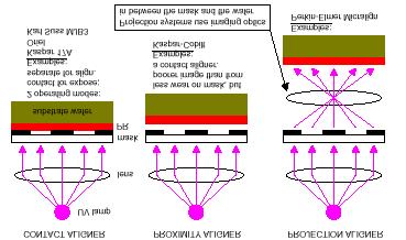
18 Softbake Removes solvent from film and stablizing coating: typical: 90C to 120C I-line DNQ 100C to 130C: DUV CAR 18

19 Alignment 19
20 Photoresist Exposure DNQ photoresist actinic radiation 20
21 DUV: Photoresist Exposure wavelengths below 200nm All use excimer lasers Note 248nm = KrF laser 21
22 Photoresist Exposure 22

23 Exposure and feature type 23

24 Positive and Negative Tone Photoresists 24
25 Contact/Proximity/Projection printing 25
26 Projection printing: Typical stepper 26
27 Projection printing: Numerical Aperture 27
28 Projection printing: High NA lens 28
29 Projection printing: Resolution 29
30 Projection printing: Depth of Focus 30
31 Projection printing: Depth of Focus 31

32 Optical lithography Performance: Resolution NA and wavelength coherent systems 32

33 Photoresist Standing waves: reflection/interference 33
34 Photoresist Post Exposure Bake Purposes: key idea DNQ/Novolak positive tone: diffusion bake : Diffusion of PAC to improve CD contact by removing standing waves. PAG/Novolak negative tone: (acid hardened resist: AHR) Diffusion of H+ ion to react with polymer causing polymer to become insoluble.( PAG: Triazine) DUV PAG/Blocking group/phs: Diffusion of H+ ion to react with blocking group causing PHS to become soluble 34
35 Photoresist exposure and dissolution Key ideas: DNQ and Novolak Resin I-line 365nm system 1. DNQ or Photo Active Compound PAC is an Inhibitor: It inhibits Development rate when present! There is very little dissolution in an OH solution. 2. Photolytic conversion of DNQ to ICA in by exposure to Near UV radiation ( Hg lamp) increases development rate PAG and Poly Hydroxystyrene PHS DUV CAR 248nm system 1. PAG Photo-Acid-Generator creates an Acid (H+) upon exposure to 248nm radiation. There is very little dissolution in an OH solution. 2. The addition of thermal energy using a PEB bake causes the H+ to diffuse and react with the blocking group, causing the exposed area to become soluble. 35
36 Photoresist Development Threshold dose Develop exposed photoresist in TMAH (2.38%) basic solution 36
37 Photoresist CDs Dose Vs linewidth Polysilicon Linewidth DUV photoresist 0 Focus offset. 0.7 Photoresist linewidth CD um y = x R 2 = ACEN ALL ALR AUL AUR ZCEN ZLL ZLR ZUL ZUR Linear (AUL) Exposure Dose 37
38 Photoresist CDs Dose Vs Spacewidth Contact CD Vs Exposure Dose Mj/cm2 IX405 i-line Photoresist Nominal 0.80u 0.95 Contact Photoresist CD microns CEN DI Linear (201CEN DI) y = x R 2 = ASML 5500/100C Exposure dose mj/cm2 38

39 I-line Positive tone Photoresist 365nm Line dense isolated line isolated space contact 39

40 I-line negative tone Photoresist 365nm 40

41 DUV Photoresist KrF 248nm 41

42 DUV Photoresist OH contamination issue 42
43 Photoresist Post-develop bake Hardbake Improve adhesion of photoresist for subsequent wet processing: Wet etches: BHF, Acetic acid, H 2 O 2 Plateup: Au or Cu Increasing hardbake temperature will cause photoresist patterns to flow. 43
44 Photoresist Etch 44

45 Photoresist Etch: RIE 45
46 Photoresist removal: Strip Post etch 46
Photolithography II ( Part 1 )
") 1 Photolithography II ( Part 1 ) Chapter 14 : Semiconductor Manufacturing Technology by M. Quirk & J. Serda Bjørn-Ove Fimland, Department of Electronics and Telecommunication, Norwegian University of Science
1 Photolithography II ( Part 1 ) Chapter 14 : Semiconductor Manufacturing Technology by M. Quirk & J. Serda Bjørn-Ove Fimland, Department of Electronics and Telecommunication, Norwegian University of Science
Chapter 3 : ULSI Manufacturing Technology - (c) Photolithography
 Photolithography") Chapter 3 : ULSI Manufacturing Technology - (c) Photolithography 1 Reference 1. Semiconductor Manufacturing Technology : Michael Quirk and Julian Serda (2001) 2. - (2004) 3. Semiconductor Physics and Devices-
Chapter 3 : ULSI Manufacturing Technology - (c) Photolithography 1 Reference 1. Semiconductor Manufacturing Technology : Michael Quirk and Julian Serda (2001) 2. - (2004) 3. Semiconductor Physics and Devices-
Methodology of modeling and simulating line-end shortening effects in deep-uv resist
 Methodology of modeling and simulating line-end shortening effects in deep-uv resist Mosong Cheng*, Ebo Croffie, Andrew Neureuther Electronics Research Laboratory Department of Electrical Engineering and
Introduction. Photoresist : Type: Structure:
 Photoresist SEM images of the morphologies of meso structures and nanopatterns on (a) a positively nanopatterned silicon mold, and (b) a negatively nanopatterned silicon mold. Introduction Photoresist
Pattern Transfer- photolithography
 Pattern Transfer- photolithography DUV : EUV : 13 nm 248 (KrF), 193 (ArF), 157 (F 2 )nm H line: 400 nm I line: 365 nm G line: 436 nm Wavelength (nm) High pressure Hg arc lamp emission Ref: Campbell: 7
Photolithography 光刻 Part II: Photoresists
 微纳光电子材料与器件工艺原理 Photolithography 光刻 Part II: Photoresists Xing Sheng 盛兴 Department of Electronic Engineering Tsinghua University xingsheng@tsinghua.edu.cn 1 Photolithography 光刻胶 负胶 正胶 4 Photolithography
Development of Lift-off Photoresists with Unique Bottom Profile
 Transactions of The Japan Institute of Electronics Packaging Vol. 8, No. 1, 2015 [Technical Paper] Development of Lift-off Photoresists with Unique Bottom Profile Hirokazu Ito, Kouichi Hasegawa, Tomohiro
MEEN Nanoscale Issues in Manufacturing. Lithography Lecture 1: The Lithographic Process
 MEEN 489-500 Nanoscale Issues in Manufacturing Lithography Lecture 1: The Lithographic Process 1 Discuss Reading Assignment 1 1 Introducing Nano 2 2 Size Matters 3 3 Interlude One-The Fundamental Science
Top down and bottom up fabrication
 Lecture 24 Top down and bottom up fabrication Lithography ( lithos stone / graphein to write) City of words lithograph h (Vito Acconci, 1999) 1930 s lithography press Photolithography d 2( NA) NA=numerical
Fabrication Engineering at the Micro- and Nanoscale, by Stephen Campbell, 4 th Edition, Oxford University Press
 Fabrication Engineering at the Micro- and Nanoscale, by Stephen Campbell, 4 th Edition, Oxford University Press Errata, by Chris Mack, chris@lithoguru.com While teaching out of this book at the University
Simulation Based Formulation of a Non-Chemically Amplified Resist for 257 nm Laser Mask Fabrication
 Simulation Based Formulation of a Non-Chemically Amplified Resist for 257 nm Laser Mask Fabrication Benjamen M. Rathsack, Cyrus E. Tabery, Timothy B. Stachowiak, Jeff Albelo 2 and C. Grant Willson Department
UNIVERSITY OF CALIFORNIA College of Engineering Department of Electrical Engineering and Computer Sciences. Professor Ali Javey. Fall 2009.
 UNIVERSITY OF CALIFORNIA College of Engineering Department of Electrical Engineering and Computer Sciences EE143 Professor Ali Javey Fall 2009 Exam 1 Name: SID: Closed book. One sheet of notes is allowed.
Effect of PAG Location on Resists for Next Generation Lithographies
 Effect of PAG Location on Resists for Next Generation Lithographies ber Research Group Materials Science & Engineering Ithaca, NY 14853 Development Trends in Microlithography 10 Contact Printer Architectures
EFFECT OF NANOSCALE CONFINEMENT ON THE PHYSICAL PROPERTIES OF POLYMER THIN FILMS
 EFFECT OF NANOSCALE CONFINEMENT ON THE PHYSICAL PROPERTIES OF POLYMER THIN FILMS A Thesis Presented to The Academic Faculty by Lovejeet Singh In Partial Fulfillment of the Requirements for the Degree Doctor
Introduction to Photolithography
 http://www.ichaus.de/news/72 Introduction to Photolithography Photolithography The following slides present an outline of the process by which integrated circuits are made, of which photolithography is
Lecture 8. Photoresists and Non-optical Lithography
 Lecture 8 Photoresists and Non-optical Lithography Reading: Chapters 8 and 9 and notes derived from a HIGHLY recommended book by Chris Mack, Fundamental Principles of Optical Lithography. Any serious student
Fabrication of Sub-Quarter-Micron Grating Patterns by Employing Lithography
 MCROU,!~'O~C ELSEVER Microelectronic Engineering 46 (1999) 173-177 Fabrication of Sub-Quarter-Micron Grating Patterns by Employing Lithography DUV Holographic L. A. Wang*, C. H. Lin and J. H. Chen nstitute
Overview of the main nano-lithography techniques
 Overview of the main nano-lithography techniques Soraya Sangiao sangiao@unizar.es Outline Introduction: Nanotechnology. Nano-lithography techniques: Masked lithography techniques: Photolithography. X-ray
UNIT 3. By: Ajay Kumar Gautam Asst. Prof. Dev Bhoomi Institute of Technology & Engineering, Dehradun
 UNIT 3 By: Ajay Kumar Gautam Asst. Prof. Dev Bhoomi Institute of Technology & Engineering, Dehradun 1 Syllabus Lithography: photolithography and pattern transfer, Optical and non optical lithography, electron,
Improving resist resolution and sensitivity via electric-field enhanced postexposure baking
 Improving resist resolution and sensitivity via electric-field enhanced postexposure baking Mosong Cheng, a) Lei Yuan, Ebo Croffie, and Andrew Neureuther Electronics Research Laboratory, University of
IC Fabrication Technology
 IC Fabrication Technology * History: 1958-59: J. Kilby, Texas Instruments and R. Noyce, Fairchild * Key Idea: batch fabrication of electronic circuits n entire circuit, say 10 7 transistors and 5 levels
DUV Positive Photoresists
 Journal of Photopolymer Science and Technology Volume 5, Number 1(1992) 207-216 Factors Affecting the Performance of Chemically DUV Positive Photoresists Amplified James W. Thackeray, Theodore H. Fedynyshyn,
Copyright 2000 by the Society of Photo-Optical Instrumentation Engineers.
 Copyright 2 by the Society of Photo-Optical Instrumentation Engineers. This paper was published in the proceedings of Photomask and X-Ray Mask Technology VII SPIE Vol. 466, pp. 172-179. It is made available
A Physically Based Model for Predicting Volume Shrinkage in Chemically Amplified Resists
 A Physically Based Model for Predicting Volume Shrinkage in Chemically Amplified Resists Nickhil Jakatdar 1, Junwei Bao, Costas J. Spanos Dept. of Electrical Engineering and Computer Sciences, University
EE C245 ME C218 Introduction to MEMS Design Fall 2007
 EE C245 ME C218 Introduction to MEMS Design Fall 2007 Prof. Clark T.-C. Nguyen Dept. of Electrical Engineering & Computer Sciences University of California at Berkeley Berkeley, CA 94720 Lecture 5: ALD,
High Optical Density Photomasks For Large Exposure Applications
 High Optical Density Photomasks For Large Exposure Applications Dan Schurz, Warren W. Flack, Makoto Nakamura Ultratech Stepper, Inc. San Jose, CA 95134 Microlithography applications such as advanced packaging,
Silicon VLSI Technology. Fundamentals, Practice and Modeling
 Text Book: Silicon VLSI Technology Fundamentals, Practice and Modeling Authors: J. D. Plummer, M. D. Deal, and P. B. Griffin Photolithography (Chap. 1) Basic lithography process Apply photoresist Patterned
Lithographic Effects Of Acid Diffusion In Chemically Amplified Resists
 INTERFACE '95 This paper was published in the proceedings of the OCG Microlithography Seminar, Interface '95, pp. 217-228. It is made available as an electronic reprint with permission of OCG Microelectronic
Lecture 150 Basic IC Processes (10/10/01) Page ECE Analog Integrated Circuits and Systems P.E. Allen
 Page ECE Analog Integrated Circuits and Systems P.E. Allen") Lecture 150 Basic IC Processes (10/10/01) Page 1501 LECTURE 150 BASIC IC PROCESSES (READING: TextSec. 2.2) INTRODUCTION Objective The objective of this presentation is: 1.) Introduce the fabrication of
Lecture 150 Basic IC Processes (10/10/01) Page 1501 LECTURE 150 BASIC IC PROCESSES (READING: TextSec. 2.2) INTRODUCTION Objective The objective of this presentation is: 1.) Introduce the fabrication of
Techniken der Oberflächenphysik (Techniques of Surface Physics)
") Techniken der Oberflächenphysik (Techniques of Surface Physics) Prof. Yong Lei & Dr. Yang Xu (& Liying Liang) Fachgebiet 3D-Nanostrukturierung, Institut für Physik Contact: yong.lei@tu-ilmenau.de; yang.xu@tu-ilmenau.de;
Techniken der Oberflächenphysik (Techniques of Surface Physics) Prof. Yong Lei & Dr. Yang Xu (& Liying Liang) Fachgebiet 3D-Nanostrukturierung, Institut für Physik Contact: yong.lei@tu-ilmenau.de; yang.xu@tu-ilmenau.de;
Lithography and Etching
 Lithography and Etching Victor Ovchinnikov Chapters 8.1, 8.4, 9, 11 Previous lecture Microdevices Main processes: Thin film deposition Patterning (lithography) Doping Materials: Single crystal (monocrystal)
Carrier Transport by Diffusion
 Carrier Transport by Diffusion Holes diffuse ÒdownÓ the concentration gradient and carry a positive charge --> hole diffusion current has the opposite sign to the gradient in hole concentration dp/dx p(x)
Optical Proximity Correction
 Optical Proximity Correction Mask Wafer *Auxiliary features added on mask 1 Overlay Errors + + alignment mask wafer + + photomask plate Alignment marks from previous masking level 2 (1) Thermal run-in/run-out
UNIVERSITY OF CALIFORNIA College of Engineering Department of Electrical Engineering and Computer Sciences. Fall Exam 1
 UNIVERSITY OF CALIFORNIA College of Engineering Department of Electrical Engineering and Computer Sciences EECS 143 Fall 2008 Exam 1 Professor Ali Javey Answer Key Name: SID: 1337 Closed book. One sheet
Wet Chemical Processing with Megasonics Assist for the Removal of Bumping Process Photomasks
 Wet Chemical Processing with Megasonics Assist for the Removal of Bumping Process Photomasks Hongseong Sohn and John Tracy Akrion Systems 6330 Hedgewood Drive, Suite 150 Allentown, PA 18106, USA Abstract
Resist Materials Issues beyond 22 nm-hp Patterning for EUV Lithography
 Resist Materials Issues beyond 22 nm-hp Patterning for EUV Lithography February 26, 2009 Shinji Tarutani FUJIFILM Corporation Research & Development Management Headquarters Electronic Materials Research
Nanostructures Fabrication Methods
 Nanostructures Fabrication Methods bottom-up methods ( atom by atom ) In the bottom-up approach, atoms, molecules and even nanoparticles themselves can be used as the building blocks for the creation of
Exploration of non-chemically amplified resists based on chain-scission mechanism for 193 nm lithography
 Rochester Institute of Technology RIT Scholar Works Theses Thesis/Dissertation Collections 2010 Exploration of non-chemically amplified resists based on chain-scission mechanism for 193 nm lithography
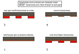
Photoresist Profile. Undercut: negative slope, common for negative resist; oxygen diffusion prohibits cross-linking; good for lift-off.
 Photoresist Profile 4-15 Undercut: negative slope, common for negative resist; oxygen diffusion prohibits cross-linking; good for lift-off undercut overcut Overcut: positive slope, common to positive resist,
Resist material for negative tone development process
 Resist material for negative tone development process FUJIFILM Corporation Electronic Materials Research Laboratories P-1 Outline 1. Advantages of negative tone imaging for DP 2. Process maturity of negative
Photomasks. Photolithography Evolution 9/11/2004 ECE580- MPE/MASKS/PHOTOMASKS.PPT
 Photolithography Evolution 1 : Evolution 2 Photomasks Substrates: Type : thermal expansion Chrome Pellicles Mask: OPC and PSM Fabrication: E-Beam or Laser 3 Photomask Information Websites: http://www.photronics.com/internet/corpcomm/publications/basics101/basics.
Chapter 2. Design and Fabrication of VLSI Devices
 Chapter 2 Design and Fabrication of VLSI Devices Jason Cong 1 Design and Fabrication of VLSI Devices Objectives: To study the materials used in fabrication of VLSI devices. To study the structure of devices
Lecture 0: Introduction
 Lecture 0: Introduction Introduction q Integrated circuits: many transistors on one chip q Very Large Scale Integration (VLSI): bucketloads! q Complementary Metal Oxide Semiconductor Fast, cheap, low power
4FNJDPOEVDUPS 'BCSJDBUJPO &UDI
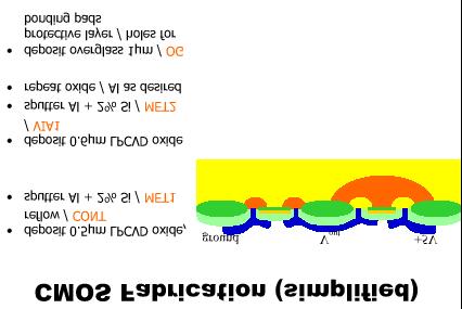
 2010.5.4 1 Major Fabrication Steps in CMOS Process Flow UV light oxygen Silicon dioxide Silicon substrate Oxidation (Field oxide) photoresist Photoresist Coating Mask exposed photoresist Mask-Wafer Exposed
Far IR Gas Lasers microns wavelengths, THz frequency Called Terahertz lasers or FIR lasers At this wavelength behaves more like
 Far IR Gas Lasers 10-1500 microns wavelengths, 300 10 THz frequency Called Terahertz lasers or FIR lasers At this wavelength behaves more like microwave signal than light Created by Molecular vibronic
520/ Photolithography (II) Andreas G. Andreou
 Andreas G. Andreou") 520/580.495 Photolithography (II) Andreas G. Andreou Lecture notes from Positive Photoresists and Photolithography by R. Darling http://www.engr.washington.edu/~cam/processes A.G. Andreou 2000 1 Lecture
520/580.495 Photolithography (II) Andreas G. Andreou Lecture notes from Positive Photoresists and Photolithography by R. Darling http://www.engr.washington.edu/~cam/processes A.G. Andreou 2000 1 Lecture
nmos IC Design Report Module: EEE 112
 nmos IC Design Report Author: 1302509 Zhao Ruimin Module: EEE 112 Lecturer: Date: Dr.Zhao Ce Zhou June/5/2015 Abstract This lab intended to train the experimental skills of the layout designing of the
FEM Modeling of Shrinkage Effects in Negative Tone Photoresists
 FEM Modeling of Shrinkage Effects in Negative Tone Photoresists Master s Thesis/Masterarbeit in the field of Computational Engineering by Sean Dominic D Silva Department Informatik Lehrstuhl für Informatik
Discussions start next week Labs start in week 3 Homework #1 is due next Friday
 EECS141 1 Discussions start next week Labs start in week 3 Homework #1 is due next Friday Everyone should have an EECS instructional account Use cory, quasar, pulsar EECS141 2 1 CMOS LEAKAGE CHARACTERIZATION
EE C245 ME C218 Introduction to MEMS Design Fall 2010
 Lecture Outline EE C245 ME C28 Introduction to MEMS Design Fall 200 Prof. Clark T.-C. Nguyen Dept. of Electrical Engineering & Computer Sciences University of California at Berkeley Berkeley, CA 94720
Swing Curves. T h e L i t h o g r a p h y T u t o r (Summer 1994) Chris A. Mack, FINLE Technologies, Austin, Texas
 Chris A. Mack, FINLE Technologies, Austin, Texas") T h e L i t h o g r a p h y T u t o r (Summer 1994) Swing Curves Chris A. Mack, FINLE Technologies, Austin, Texas In the last edition of this column, we saw that exposing a photoresist involves the propagation
T h e L i t h o g r a p h y T u t o r (Summer 1994) Swing Curves Chris A. Mack, FINLE Technologies, Austin, Texas In the last edition of this column, we saw that exposing a photoresist involves the propagation
EE 434 Lecture 7. Process Technology
 EE 434 Lecture 7 Process Technology Quiz 4 How many wafers can be obtained from a 2m pull? Neglect the material wasted in the kerf used to separate the wafers. 2m And the number is. 1 8 3 5 6 4 9 7 2 1
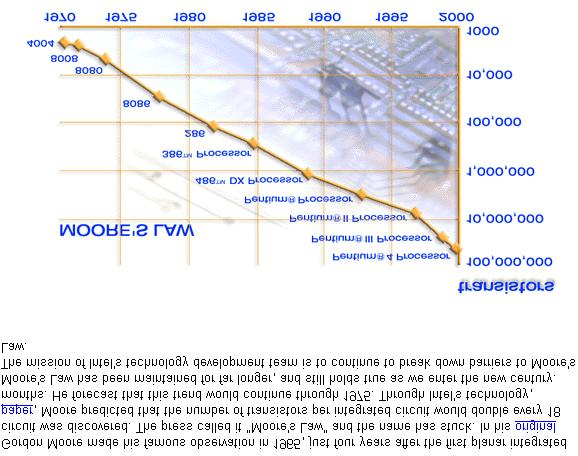
Lithography Challenges Moore s Law Rising Costs and Challenges of Advanced Patterning
 Lithography Challenges Moore s Law Rising Costs and Challenges of Advanced Patterning SEMI Texas Spring Forum May 21, 2013 Austin, Texas Author / Company / Division / Rev. / Date A smartphone today has
UNIVERSITY OF CALIFORNIA College of Engineering Department of Electrical Engineering and Computer Sciences. Professor Ali Javey. Spring 2009.
 UNIVERSITY OF CALIFORNIA College of Engineering Department of Electrical Engineering and Computer Sciences EE143 Professor Ali Javey Spring 2009 Exam 1 Name: SID: Closed book. One sheet of notes is allowed.
Title: ASML Stepper Semiconductor & Microsystems Fabrication Laboratory Revision: B Rev Date: 12/21/2010
 Approved by: Process Engineer / / / / Equipment Engineer 1 SCOPE The purpose of this document is to detail the use of the ASML PAS 5500 Stepper. All users are expected to have read and understood this
J. Photopolym. Sci. Technol., Vol. 22, No. 5, Fig. 1. Orthogonal solvents to conventional process media.
 originates from the limited number of options regarding orthogonal solvents, i.e. solvents that do not dissolve or adversely damage a pre-deposited organic materials layer. The simplest strategy to achieve
5. Photochemistry of polymers
 5. Photochemistry of polymers 5.1 Photopolymerization and cross-linking Photopolymerization The fundamental principle of photopolymerization is based on the photoinduced production of a reactive species,
Self-study problems and questions Processing and Device Technology, FFF110/FYSD13
 Self-study problems and questions Processing and Device Technology, FFF110/FYSD13 Version 2016_01 In addition to the problems discussed at the seminars and at the lectures, you can use this set of problems
EE115C Winter 2017 Digital Electronic Circuits. Lecture 3: MOS RC Model, CMOS Manufacturing
 EE115C Winter 2017 Digital Electronic Circuits Lecture 3: MOS RC Model, CMOS Manufacturing Agenda MOS Transistor: RC Model (pp. 104-113) S R on D CMOS Manufacturing Process (pp. 36-46) S S C GS G G C GD
Far IR (FIR) Gas Lasers microns wavelengths, THz frequency Called Terahertz lasers or FIR lasers At this wavelength behaves more like
 Gas Lasers microns wavelengths, THz frequency Called Terahertz lasers or FIR lasers At this wavelength behaves more like") Far IR (FIR) Gas Lasers 10-1500 microns wavelengths, 300 10 THz frequency Called Terahertz lasers or FIR lasers At this wavelength behaves more like microwave signal than light Created by Molecular vibronic
Far IR (FIR) Gas Lasers 10-1500 microns wavelengths, 300 10 THz frequency Called Terahertz lasers or FIR lasers At this wavelength behaves more like microwave signal than light Created by Molecular vibronic
Composition and Photochemical Mechanisms of Photoresists
 OpenStax-CNX module: m25525 1 Composition and Photochemical Mechanisms of Photoresists Andrew R. Barron This work is produced by OpenStax-CNX and licensed under the Creative Commons Attribution License
Current Status of Inorganic Nanoparticle Photoresists
 Prof. Christopher K. ber Department of Materials Science and Engineering, Cornell University, Ithaca NY Current Status of Inorganic Nanoparticle Photoresists Markos Trikeriotis, Marie Krysak, Yeon Sook
Recent progress in nanoparticle photoresist development for EUV lithography
 Recent progress in nanoparticle photoresist development for EUV lithography Kazuki Kasahara ab, Vasiliki Kosma b, Jeremy Odent b, Hong Xu b, Mufei Yu b, Emmanuel P. Giannelis b, Christopher K. Ober b a
Chapter 3 Basics Semiconductor Devices and Processing
 Chapter 3 Basics Semiconductor Devices and Processing Hong Xiao, Ph. D. www2.austin.cc.tx.us/hongxiao/book.htm Hong Xiao, Ph. D. www2.austin.cc.tx.us/hongxiao/book.htm 1 Objectives Identify at least two
Lecture 14 Advanced Photolithography
 Lecture 14 Advanced Photolithography Chapter 14 Wolf and Tauber 1/74 Announcements Term Paper: You are expected to produce a 4-5 page term paper on a selected topic (from a list). Term paper contributes
Study on Improved Resolution of Thick Film Resist (Verification by Simulation)
") Study on Improved Resolution of Thick Film Resist (Verification by Simulation) Yoshihisa Sensu, Atsushi Sekiguchi, Yasuhiro Miyake Litho Tech Japan Corporation 2-6-6 Namiki, Kawaguchi, Saitama, 332-0034,
Study on Improved Resolution of Thick Film Resist (Verification by Simulation) Yoshihisa Sensu, Atsushi Sekiguchi, Yasuhiro Miyake Litho Tech Japan Corporation 2-6-6 Namiki, Kawaguchi, Saitama, 332-0034,
Copyright 1999 by the Society of Photo-Optical Instrumentation Engineers.
 Copyright 1999 by the Society of Photo-Optical Instrumentation Engineers. This paper was published in the proceedings of Advances in Resist Technology and Processing XVI, SPIE Vol. 3678, pp. 1-1011. It
Copyright 1999 by the Society of Photo-Optical Instrumentation Engineers.
 Copyright 1999 by the Society of Photo-Optical Instrumentation Engineers. This paper was published in the proceedings of Lithography for Semiconductor Manufacturing SPIE Vol. 3741, pp. 148-160. It is made
Far IR (FIR) Gas Lasers microns wavelengths, THz frequency Called Terahertz lasers or FIR lasers At this wavelength behaves more like
 Gas Lasers microns wavelengths, THz frequency Called Terahertz lasers or FIR lasers At this wavelength behaves more like") Far IR (FIR) Gas Lasers 10-1500 microns wavelengths, 300 10 THz frequency Called Terahertz lasers or FIR lasers At this wavelength behaves more like microwave signal than light Created by Molecular vibronic
Far IR (FIR) Gas Lasers 10-1500 microns wavelengths, 300 10 THz frequency Called Terahertz lasers or FIR lasers At this wavelength behaves more like microwave signal than light Created by Molecular vibronic
EE143 LAB. Professor N Cheung, U.C. Berkeley
 EE143 LAB 1 1 EE143 Equipment in Cory 218 2 Guidelines for Process Integration * A sequence of Additive and Subtractive steps with lateral patterning Processing Steps Si wafer Watch out for materials compatibility
EE141- Spring 2003 Lecture 3. Last Lecture
 - Spring 003 Lecture 3 IC Manufacturing 1 Last Lecture Design Metrics (part 1) Today Design metrics (wrap-up) IC manufacturing 1 Administrivia Discussion sessions start this week. Only one this week (Dejan
A Parameter Extraction Framework for DUV Lithography Simulation
 A Parameter Extraction Framework for DUV Lithography Simulation Nickhil Jakatdar 1, Junwei Bao, Costas J. Spanos Dept. of Electrical Engineering and Computer Sciences, University of California at Berkeley,
Chen et al. (45) Date of Patent: Dec. 5, (54) EFFECTIVE PHOTORESIST STRIPPING (56) References Cited
 Date of Patent: Dec. 5, (54) EFFECTIVE PHOTORESIST STRIPPING (56) References Cited") (12) United States Patent USOO7144673B2 (10) Patent No.: US 7,144.673 B2 Chen et al. (45) Date of Patent: Dec. 5, 2006 (54) EFFECTIVE PHOTORESIST STRIPPING (56) References Cited PROCESS FOR HIGH DOSAGE
(12) United States Patent USOO7144673B2 (10) Patent No.: US 7,144.673 B2 Chen et al. (45) Date of Patent: Dec. 5, 2006 (54) EFFECTIVE PHOTORESIST STRIPPING (56) References Cited PROCESS FOR HIGH DOSAGE
Next: 193nm Lithography
 Lecture 16 Chemical Engineering for Micro/Nano Fabrication Next: 193nm Lithography Absorption coefficient [1/µm] Absorption of Photoresist Polymers 2.8 Poly-(4-hydroxystyrene) 2.4 Meta-cresol novolak 2.0
EE C245 ME C218 Introduction to MEMS Design
 EE C245 ME C218 Introduction to MEMS Design Fall 2008 Prof. Clark T.-C. Nguyen Dept. of Electrical Engineering & Computer Sciences University of California at Berkeley Berkeley, CA 94720 Lecture 6: Process
Dainippon Screen Mfg. Co., Ltd , Takamiya, Hikone, Shiga , Japan. IMEC vzw, Kapeldreef 75, B-3001 Leuven, Belgium
 Solid State Phenomena Vols. 145-146 (2009) pp 285-288 Online available since 2009/Jan/06 at www.scientific.net (2009) Trans Tech Publications, Switzerland doi:10.4028/www.scientific.net/ssp.145-146.285
Fabrication Technology, Part I
 EEL5225: Principles of MEMS Transducers (Fall 2004) Fabrication Technology, Part I Agenda: Microfabrication Overview Basic semiconductor devices Materials Key processes Oxidation Thin-film Deposition Reading:
Functional Materials for Advanced Patterning Robert D. Allen. IBM Almaden Research Center
 Functional Materials for Advanced Patterning Robert D. Allen Business Unit or Product Name IBM Almaden Research Center 2003 IBM Corporation Resists/Materials for Advanced Patterning Trends in Lithography
CHAPTER 6: Etching. Chapter 6 1
 Chapter 6 1 CHAPTER 6: Etching Different etching processes are selected depending upon the particular material to be removed. As shown in Figure 6.1, wet chemical processes result in isotropic etching
Figure 1: Graphene release, transfer and stacking processes. The graphene stacking began with CVD
 Supplementary figure 1 Graphene Growth and Transfer Graphene PMMA FeCl 3 DI water Copper foil CVD growth Back side etch PMMA coating Copper etch in 0.25M FeCl 3 DI water rinse 1 st transfer DI water 1:10
Techniques for directly measuring the absorbance of photoresists at EUV wavelengths
 Techniques for directly measuring the absorbance of photoresists at EUV wavelengths Manish Chandhok, a Heidi Cao, a Wang Yueh, a Eric Gullikson, b Robert Brainard, c Stewart Robertson c a Intel Corporation,
Supplementary Information
 Supplementary Information Experimental Section Hybrid Nanoparticle Synthesis The hafnium nanoparticles surface-modified with methacrylic acid (MAA, Sigma Aldrich, 99%), trans 2, 3-dimethylacrylic acid
Nano fabrication by e-beam lithographie
 Introduction to nanooptics, Summer Term 2012, Abbe School of Photonics, FSU Jena, Prof. Thomas Pertsch Nano fabrication by e-beam lithographie Lecture 14 1 Electron Beam Lithography - EBL Introduction
Woo Jin Hyun, Ethan B. Secor, Mark C. Hersam, C. Daniel Frisbie,* and Lorraine F. Francis*
 Woo Jin Hyun, Ethan B. Secor, Mark C. Hersam, C. Daniel Frisbie,* and Lorraine F. Francis* Dr. W. J. Hyun, Prof. C. D. Frisbie, Prof. L. F. Francis Department of Chemical Engineering and Materials Science
Thin Wafer Handling Challenges and Emerging Solutions
 1 Thin Wafer Handling Challenges and Emerging Solutions Dr. Shari Farrens, Mr. Pete Bisson, Mr. Sumant Sood and Mr. James Hermanowski SUSS MicroTec, 228 Suss Drive, Waterbury Center, VT 05655, USA 2 Thin
EE-612: Lecture 22: CMOS Process Steps
 EE-612: Lecture 22: CMOS Process Steps Mark Lundstrom Electrical and Computer Engineering Purdue University West Lafayette, IN USA Fall 2006 NCN www.nanohub.org Lundstrom EE-612 F06 1 outline 1) Unit Process
Developer-soluble Gap fill materials for patterning metal trenches in Via-first Dual Damascene process
 Developer-soluble Gap fill materials for patterning metal trenches in Via-first Dual Damascene process Mandar Bhave, Kevin Edwards, Carlton Washburn Brewer Science, Inc., 2401 Brewer Dr., Rolla, MO 65401,
Micro- and Nano-Technology... for Optics
 Micro- and Nano-Technology...... for Optics U.D. Zeitner Fraunhofer Institut für Angewandte Optik und Feinmechanik Jena Today: 1. Introduction E. Bernhard Kley Institute of Applied Physics Friedrich-Schiller
DIFFUSION OF ACID AND ACTIVATION ENERGY OF POSITIVE CHEMICAL AMPLIFICATION RESIST
 Journal of Photopolymer Science and Technology Volume 6, Number 4(1993) 505-514 1993TAPJ DIFFUSION OF ACID AND ACTIVATION ENERGY OF POSITIVE CHEMICAL AMPLIFICATION RESIST Koi 7ASAKAWA Toshiba Research
Characterization of Optical Proximity Correction Features
 Characterization of Optical Proximity Correction Features John Allgair, Michelle Ivy, Kevin Lucas, John Sturtevant Motorola APRDL, Austin, TX 7871 Richard Elliott, Chris A. Mack, Craig MacNaughton, John
Line-Edge Roughness and the Impact of Stochastic Processes on Lithography Scaling for Moore s Law
 Line-Edge Roughness and the Impact of Stochastic Processes on Lithography Scaling for Moore s Law Chris A. Mack Lithoguru.com, 1605 Watchhill Rd, Austin, TX 78703 Abstract Moore s Law, the idea that every
EE 434 Lecture 12. Process Flow (wrap up) Device Modeling in Semiconductor Processes
 Device Modeling in Semiconductor Processes") EE 434 Lecture 12 Process Flow (wrap up) Device Modeling in Semiconductor Processes Quiz 6 How have process engineers configured a process to assure that the thickness of the gate oxide for the p-channel
EE 434 Lecture 12 Process Flow (wrap up) Device Modeling in Semiconductor Processes Quiz 6 How have process engineers configured a process to assure that the thickness of the gate oxide for the p-channel
Photonics applications 5: photoresists
 IMI-NFG s Mini Course on Chalcogenide Glasses Lecture 11 Photonics applications 5: photoresists Himanshu Jain Department of Materials Science & Engineering Lehigh University, Bethlehem, PA 18015 H.Jain@Lehigh.edu
Copyright 2001 by the Society of Photo-Optical Instrumentation Engineers.
 Copyright 2001 by the Society of Photo-Optical Instrumentation Engineers. This paper was published in the proceedings of Lithography for Semiconductor Manufacturing SPIE Vol. 4404, pp. 111-122. It is made
Supplementary Figure 1 Detailed illustration on the fabrication process of templatestripped
 Supplementary Figure 1 Detailed illustration on the fabrication process of templatestripped gold substrate. (a) Spin coating of hydrogen silsesquioxane (HSQ) resist onto the silicon substrate with a thickness
Copyright 1997 by the Society of Photo-Optical Instrumentation Engineers.
 Copyright 1997 by the Society of Photo-Optical Instrumentation Engineers. This paper was published in the proceedings of Advances in Resist Technology and Processing XIV, SPIE Vol. 3049, pp. 706-711. It
Fabrication Technology for Miniaturization
 Appendix A Fabrication Technology for Miniaturization INTRODUCTION Many of the technologies that have enabled advances in miniaturization were first developed for microelectronics and allow both lateral
Clean-Room microfabrication techniques. Francesco Rizzi Italian Institute of Technology
 Clean-Room microfabrication techniques Francesco Rizzi Italian Institute of Technology Miniaturization The first transistor Miniaturization The first transistor Miniaturization The first transistor Miniaturization
EUVL Readiness for High Volume Manufacturing
 EUVL Readiness for High Volume Manufacturing Britt Turkot Intel Corporation Outline Exposure Tool Progress Power Availability Intel demo results Reticle Defectivity Pellicle Materials Conclusion 2 Source
Study of Line Edge Roughness and Interactions of Secondary Electrons in Photoresists for EUV Lithography
 Study of Line Edge Roughness and Interactions of Secondary Electrons in Photoresists for EUV Lithography Suchit Bhattarai Electrical Engineering and Computer Sciences University of California at Berkeley