Lithography and Etching
|
|
|
- Shanon Bryan
- 5 years ago
- Views:
Transcription
1 Lithography and Etching Victor Ovchinnikov Chapters 8.1, 8.4, 9, 11
2 Previous lecture Microdevices Main processes: Thin film deposition Patterning (lithography) Doping Materials: Single crystal (monocrystal) Polycrystals Thin film Process flow Cleanroom Yield Aalto Nanofab 2018 Microfabrication: lecture 2 2
3 Outline Optical lithography Beam lithography: e-beam writing laser writing focused ion beam Etching: wet etching plasma etching Aalto Nanofab 2018 Microfabrication: lecture 2 3


4 How do we create images? Direct writing Drawing Nanoimprint Embossing Photolithography Shadow mask Offset printing Stencil process 2016 Willson Research Group, The University of Texas at Austin Aalto Nanofab 2018 Microfabrication: lecture 2 4


5 Photolithography results Microfluidic chip Intel 80286, a 16-bit microcontroller Critical dimension 50 μm Chip size 50 x 50 mm Glass substrate Critical dimension 1.5 μm Chip size 7 x 7 mm Silicon substrate Aalto Nanofab 2018 Microfabrication: lecture 2 5
6 The photolithography patterning PR PR Substrate Exposed PR SiO 2 Three parts in one: Cross-linked PR Optics - exposure Chemistry - development Mechanics - alignment Aalto Nanofab 2018 Microfabrication: lecture 2 6

7 PR mask after etching Sensors and Actuators A: Physical Volume 156, Issue 1, November 2009, Pages Aalto Nanofab 2018 Microfabrication: lecture 2 7
8 Patterning terminology Photolithography - photoresist pattern Etching - transfer of photoresist pattern into solid material Stripping - removal of photoresist after etching the pattern Photomask fabricated image on transparent holder in 1x scale Patterning lithography + etching Aalto Nanofab 2018 Microfabrication: lecture 2 8

9 Lithography steps Lithography room Outgoing wafers Deposit new layer Strip resist Etch Adhesion promotion Apply photoresist Pre-bake Align Exposure Post exposure bake Develop Rinse and Dry Baking 30 minutes, 150 C, HMDS Spin-on, spray, dip, roller. 1.5 µm 90 C, 1 min - hotplate, 20 min convection furnace Maskaligner, 1-2 seconds, UV 105 C, 20 min convection furnace 1 min wetbench, 5 min spin rinse drier Post bake 120 C, 1 min - hotplate, 20 min convection furnace Incoming wafers Inspect Measure Humidity 40%, temp. 22±0.5 C Possible rework Aalto Nanofab 2018 Microfabrication: lecture 2 9

10 Spin-on Static dispense, 1-10ml Chuck Photoresist Wafer Spread cycle Skinning Liquid resist Ramp-up Liquid resist expelled from beneath the surface skin Final spin coat speed Film thickness 100 nm 500 µm Evaporation of residual solvent Aalto Nanofab 2018 Microfabrication: lecture 2 10
11 Spin coating thickness of PR air rotates with chuck air unmovable Aalto Nanofab 2018 Microfabrication: lecture 2 11

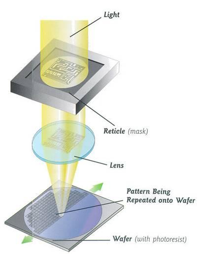
12 Three types of lithography Mask contamination, Mask damage Intact mask Low resolution High resolution Exposure of small area Stepper Aalto Nanofab 2018 Microfabrication: lecture 2 12
13 Proximity lithography Valid for λ < g < 2 b λ λ = 365 nm, i-line d = 1.4 µm (standard resist) b 0.6 µm b 2.3 µm g = 0 (contact) g = 10 µm (proximity) b is half-pitch Can be improved by phase-shift mask Aalto Nanofab 2018 Microfabrication: lecture 2 13

14 Alignment and overlay Features on wafer Alignment marks Features on mask CMOS inverter Mask over wafer Features on wafer Si P ~ C/3 Doped Si Al Aalto Nanofab 2018 Microfabrication: lecture 2 14

15 MICRONOVA maskaligner 365 nm, i-line, Hg Aalto Nanofab 2018 Microfabrication: lecture 2 15
16 Summary I Photolithography provides: required CD exact control over shape and size easy alignment parallel processing, i.e., patterns over an entire surface at the same time Limitations of photolithography works only on flat surface only 2D shapes can be generated Aalto Nanofab 2018 Microfabrication: lecture 2 16
17 Photomask fabrication Cr deposition and resist application Pattern writing by e-beam or laser PR development, Cr etching, PR stripping CD control Inspection of defects and fidelity Soft error reduction (particle removal) Reparing by ion beam (etching or deposition) Final inspection Aalto Nanofab 2018 Microfabrication: lecture 2 17

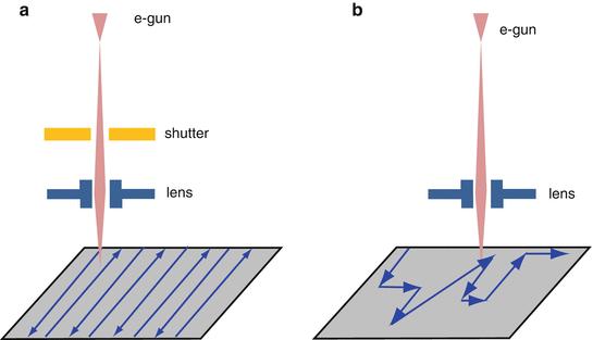
18 Pattern generation by e-beam tool e-gun shutter e-gun Applying of e-beam resist A pattern generation tool transcribes the circuit design data into a physical structure. Raster scan vs. vector scanning. Variable shaped beam vs. Gaussian beam. Shaped beam Raster scan Vector scan Global alignment vs. chipalignment. Aalto Nanofab 2018 Microfabrication: lecture 2 18


19 Laser beam sweep and a laser writer Laser beam Four laser beams Stage movement CD 500 nm Area 1x1 cm 2 Time 2 hours MICRONOVA laser writer Beam wavelength 405 nm Aalto Nanofab 2018 Microfabrication: lecture 2 19


20 Focused ion beam (FIB) MICRONOVA FIB Fabricated by FIB 3D patterning! DOI: /S Aalto Nanofab 2018 Microfabrication: lecture 2 20
21 Summary II Direct writing pros: extremly small patterns photomask is not required Direct writing cons: serial processing, i.e., one element after another alignment is problematic Aalto Nanofab 2018 Microfabrication: lecture 2 21
22 Lithography and etching 1) photoresist patterning Selectivity 2) Etching with reactive chemicals (acids, bases, plasmas) <Si> Same procedure applies both to etching thin films and to etching silicon wafer itself. Thicknesses and etch stop vary! Etching thin film Photolithography can be redone if problems detected, but after etching no repair is available. <Si> Time control Etching bulk silicon Aalto Nanofab 2018 Microfabrication: lecture 2 22
23 Etching terminology Etching mask patterned protective layer on the top of etched material Undercut lateral erosion of etched material below protective layer Selectivity ratio of etching rates for two etched materials Aspect ration ratio of height to width for a microstructure Anisotropy different etching rate in different directions Aalto Nanofab 2018 Microfabrication: lecture 2 23
24 Etch mask Protective layer that is very slowly attacked by etchant Resist is the simplest etch mask to use always consider resist mask first Aggressive etchants (KOH) will prevent use of resist hard mask required Quiz: what is a photomask? How does it relate to etch mask? Aalto Nanofab 2018 Microfabrication: lecture 2 24

25 Proceeds as a spherical wave Isotropic etching Undercuts structures (proceeds under mask) Most wet etching processes are isotropic, e.g., HF etching of oxide, H 3 PO 4 etching of Al Some of dry etchings are isotropic, e.g., photoresist stripping Undercut Undercut Undercut SiN Si 5 µm deep, isotropic etch Aalto Nanofab 2018 Microfabrication: lecture 2 25

26 Selectivity Selectivity is defined as etch rate ratio: S= rate film / rate mask = y/x Silicon etch rate 500 nm/min Oxide etch rate 15 nm/min Selectivity 33:1 Silicon etch rate 500 nm/min Resist etch rate 200 nm/min Selectivity 2.5:1 S There is always some unintentional loss of material Aalto Nanofab 2018 Microfabrication: lecture 2 26


27 Aspect ratio AR is the ratio of height to width Si pillar array AR 5:1 Si nanopillar AR 15:1 Lauri Sainiemi Nikolai Chekurov Aalto Nanofab 2018 Microfabrication: lecture 2 27
28 Main methods of etching Wet etching (usually, isotropic) solid + liquid etchant soluble products Si (s) + 2 OH H 2 O Si(OH) 2 (O - ) 2 (aq) + 2 H 2 (g) Plasma (dry) etching (usually, anisotropic) solid + gaseous etchant volatile products SiO 2 (s) + CF 4 (g) SiF 4 (g) + CO 2 (g) Typical etching rate nm/min in both cases Aalto Nanofab 2018 Microfabrication: lecture 2 28
29 Wet etchants for common materials SiO 2 HF <Si> KOH (10-50%) anisotropic etch <Si> HNO 3 :HF:CH 3 COOH isotropic etch poly-si HNO 3 :HF: H 2 O Al H 3 PO 4 :HNO 3 :H 2 O W, TiW H 2 O 2 :H 2 O Cu HNO 3 :H 2 O (1:1) Ni HNO 3 :CH 3 COOH:H 2 SO 4 Au KI:I 2 :H 2 O Pt, Au HNO 3 :HCl (1:3) aqua regia Everywhere, exclude Si etching, photoresist mask can be used Aalto Nanofab 2018 Microfabrication: lecture 2 29
 Isotropic HF wet")

30 Undercutting in action: dome resonator SiO 2 Poly 1) RIE etching of a small hole in polysilicon 2) Isotropic HF wet etching of oxide under polysilicon Membrane can move H. G. Craighead Aalto Nanofab 2018 Microfabrication: lecture 2 30
31 Anisotropic wet etching (only for crystals) Anisotropic etching Isotropic etching 54.7 Max depth is limited by lateral dimension Accurate, but limited in shape; Excellent surface finish Aalto Nanofab 2018 Microfabrication: lecture 2 31
32 Wet etching Usually isotropic, but can be anisotropic for crystals, e.g., for c-si Perfect selectivity Special etchant for each material Surface finish smooth Fast, because batch process Cheap equipment Aalto Nanofab 2018 Microfabrication: lecture 2 32


33 Dry etching RIE - Reactive Ion Etching PE - Plasma Etching, also PECVD Ion density ions/cm -3 Reactive neutrals or active radicals density ions/cm -3 Aalto Nanofab 2018 Microfabrication: lecture 2 33

34 Plasma surface interaction in RIE Aalto Nanofab 2018 Microfabrication: lecture 2 34
35 Chemistry of dry etching Material Etch gas Product gases Silicon SF 6 (or Cl 2 ) SiF 4, SiCl 4 Oxide CHF 3 (or C 4 F 8 ) SiF 4, CO 2 Nitride SF 6 (or CF 4 ) SiF 4, N 2 Aluminum Cl 2 AlCl 3 Tungsten SF 6 WF 6 Copper no practical plasma etching (Ar) Aalto Nanofab 2018 Microfabrication: lecture 2 35
")


36 Plasma etched (anisotropic) profiles Franssila: Microfabrication Aalto Nanofab 2018 Microfabrication: lecture 2 36
37 Plasma etching Usually anisotropic, but can be isotropic Near vertical walls Low selectivity Surface finish rough Slow, because single wafer process? Expensive equipment Aalto Nanofab 2018 Microfabrication: lecture 2 37


38 Wet etching vs. plasma etch I Wet etching: chemical reaction; simple wet bench and acids or bases needed Plasma etching: chemical and physical processes; requires RF-generator, vacuum system and gas lines Aalto Nanofab 2018 Microfabrication: lecture 2 38
39 Wet etch vs. plasma etch II Oxide wet etch in HF Oxide plasma etch in CHF 3 Undercut, isotropic Vertical walls, no undercut Film removed from backside Film remains on backside Aalto Nanofab 2018 Microfabrication: lecture 2 39
40 Photoresist as an etch mask Most simple to use Tolerates RIE: selectivity 10:1 at best Does not tolerate long RIE Does not tolerate most wet etchants such as KOH photomask PR mask photoresist Lithography: Photoresist spinning Lithography: UV-exposure Photoresist development Etching with resist mask Aalto Nanofab 2018 Microfabrication: lecture 2 40
41 SiO 2 Hard mask photoresist photomask <Si> Cleaned silicon wafer Thermal 1100 C Undercut Lithography: Photoresist spinning SiO 2 hard mask Lithography: UVexposure Photoresist development HF etching of SiO 2 Photoresist removal Plasma etching Aalto Nanofab 2018 Microfabrication: lecture 2 41
42 Misalignment Etching of two-layer films P RIE profile Isotropic <Si> Ideal case Ideal case Ideal case If two layers are perfectly aligned, they were made in the same etch step. Otherwise alignment error would be visible. Aalto Nanofab 2018 Microfabrication: lecture 2 42


43 Etchback Two layers surface planarization SiO 2 etching One layer surface planarization h 1 SiO 2 PR h 2 h 1 >= h 2 PR removal Planarization Spin-on glass Etchback Requirement: etching rates of glass and PR must be equal!!! Aalto Nanofab 2018 Microfabrication: lecture 2 43
4FNJDPOEVDUPS 'BCSJDBUJPO &UDI
 2010.5.4 1 Major Fabrication Steps in CMOS Process Flow UV light oxygen Silicon dioxide Silicon substrate Oxidation (Field oxide) photoresist Photoresist Coating Mask exposed photoresist Mask-Wafer Exposed
UNIT 3. By: Ajay Kumar Gautam Asst. Prof. Dev Bhoomi Institute of Technology & Engineering, Dehradun
 UNIT 3 By: Ajay Kumar Gautam Asst. Prof. Dev Bhoomi Institute of Technology & Engineering, Dehradun 1 Syllabus Lithography: photolithography and pattern transfer, Optical and non optical lithography, electron,
Section 3: Etching. Jaeger Chapter 2 Reader
 Section 3: Etching Jaeger Chapter 2 Reader Etch rate Etch Process - Figures of Merit Etch rate uniformity Selectivity Anisotropy d m Bias and anisotropy etching mask h f substrate d f d m substrate d f
Lecture 150 Basic IC Processes (10/10/01) Page ECE Analog Integrated Circuits and Systems P.E. Allen
 Page ECE Analog Integrated Circuits and Systems P.E. Allen") Lecture 150 Basic IC Processes (10/10/01) Page 1501 LECTURE 150 BASIC IC PROCESSES (READING: TextSec. 2.2) INTRODUCTION Objective The objective of this presentation is: 1.) Introduce the fabrication of
Lecture 150 Basic IC Processes (10/10/01) Page 1501 LECTURE 150 BASIC IC PROCESSES (READING: TextSec. 2.2) INTRODUCTION Objective The objective of this presentation is: 1.) Introduce the fabrication of
UNIVERSITY OF CALIFORNIA College of Engineering Department of Electrical Engineering and Computer Sciences. Fall Exam 1
 UNIVERSITY OF CALIFORNIA College of Engineering Department of Electrical Engineering and Computer Sciences EECS 143 Fall 2008 Exam 1 Professor Ali Javey Answer Key Name: SID: 1337 Closed book. One sheet
Reactive Ion Etching (RIE)
") Reactive Ion Etching (RIE) RF 13.56 ~ MHz plasma Parallel-Plate Reactor wafers Sputtering Plasma generates (1) Ions (2) Activated neutrals Enhance chemical reaction 1 2 Remote Plasma Reactors Plasma Sources
Reactive Ion Etching (RIE) RF 13.56 ~ MHz plasma Parallel-Plate Reactor wafers Sputtering Plasma generates (1) Ions (2) Activated neutrals Enhance chemical reaction 1 2 Remote Plasma Reactors Plasma Sources
EE 527 MICROFABRICATION. Lecture 24 Tai-Chang Chen University of Washington
 EE 527 MICROFABRICATION Lecture 24 Tai-Chang Chen University of Washington EDP ETCHING OF SILICON - 1 Ethylene Diamine Pyrocatechol Anisotropy: (100):(111) ~ 35:1 EDP is very corrosive, very carcinogenic,
CHAPTER 6: Etching. Chapter 6 1
 Chapter 6 1 CHAPTER 6: Etching Different etching processes are selected depending upon the particular material to be removed. As shown in Figure 6.1, wet chemical processes result in isotropic etching
Pattern Transfer- photolithography
 Pattern Transfer- photolithography DUV : EUV : 13 nm 248 (KrF), 193 (ArF), 157 (F 2 )nm H line: 400 nm I line: 365 nm G line: 436 nm Wavelength (nm) High pressure Hg arc lamp emission Ref: Campbell: 7
Etching: Basic Terminology
 Lecture 7 Etching Etching: Basic Terminology Introduction : Etching of thin films and sometimes the silicon substrate are very common process steps. Usually selectivity, and directionality are the first
DQN Positive Photoresist
 UNIVESITY OF CALIFONIA, BEKELEY BEKELEY DAVIS IVINE LOS ANGELES IVESIDE SAN DIEGO SAN FANCISCO SANTA BABAA SANTA CUZ DEPATMENT OF BIOENGINEEING 94720-1762 BioE 121 Midterm #1 Solutions BEKELEY, CALIFONIA
Device Fabrication: Etch
 Device Fabrication: Etch 1 Objectives Upon finishing this course, you should able to: Familiar with etch terminology Compare wet and dry etch processes processing and list the main dry etch etchants Become
Chapter 3 : ULSI Manufacturing Technology - (c) Photolithography
 Photolithography") Chapter 3 : ULSI Manufacturing Technology - (c) Photolithography 1 Reference 1. Semiconductor Manufacturing Technology : Michael Quirk and Julian Serda (2001) 2. - (2004) 3. Semiconductor Physics and Devices-
Chapter 3 : ULSI Manufacturing Technology - (c) Photolithography 1 Reference 1. Semiconductor Manufacturing Technology : Michael Quirk and Julian Serda (2001) 2. - (2004) 3. Semiconductor Physics and Devices-
ETCHING Chapter 10. Mask. Photoresist
 ETCHING Chapter 10 Mask Light Deposited Substrate Photoresist Etch mask deposition Photoresist application Exposure Development Etching Resist removal Etching of thin films and sometimes the silicon substrate
IC Fabrication Technology
 IC Fabrication Technology * History: 1958-59: J. Kilby, Texas Instruments and R. Noyce, Fairchild * Key Idea: batch fabrication of electronic circuits n entire circuit, say 10 7 transistors and 5 levels
Etching Issues - Anisotropy. Dry Etching. Dry Etching Overview. Etching Issues - Selectivity
 Etching Issues - Anisotropy Dry Etching Dr. Bruce K. Gale Fundamentals of Micromachining BIOEN 6421 EL EN 5221 and 6221 ME EN 5960 and 6960 Isotropic etchants etch at the same rate in every direction mask
Fabrication Technology, Part I
 EEL5225: Principles of MEMS Transducers (Fall 2004) Fabrication Technology, Part I Agenda: Microfabrication Overview Basic semiconductor devices Materials Key processes Oxidation Thin-film Deposition Reading:
EE C245 ME C218 Introduction to MEMS Design Fall 2007
 EE C245 ME C218 Introduction to MEMS Design Fall 2007 Prof. Clark T.-C. Nguyen Dept. of Electrical Engineering & Computer Sciences University of California at Berkeley Berkeley, CA 94720 Lecture 12: Mechanics
Wet and Dry Etching. Theory
 Wet and Dry Etching Theory 1. Introduction Etching techniques are commonly used in the fabrication processes of semiconductor devices to remove selected layers for the purposes of pattern transfer, wafer
LECTURE 5 SUMMARY OF KEY IDEAS
 LECTURE 5 SUMMARY OF KEY IDEAS Etching is a processing step following lithography: it transfers a circuit image from the photoresist to materials form which devices are made or to hard masking or sacrificial
EE 527 MICROFABRICATION. Lecture 25 Tai-Chang Chen University of Washington
 EE 527 MICROFABRICATION Lecture 25 Tai-Chang Chen University of Washington ION MILLING SYSTEM Kaufmann source Use e-beam to strike plasma A magnetic field applied to increase ion density Drawback Low etch
Lecture 15 Etching. Chapters 15 & 16 Wolf and Tauber. ECE611 / CHE611 Electronic Materials Processing Fall John Labram 1/76
 Lecture 15 Etching Chapters 15 & 16 Wolf and Tauber 1/76 Announcements Term Paper: You are expected to produce a 4-5 page term paper on a selected topic (from a list). Term paper contributes 25% of course
EE 143 MICROFABRICATION TECHNOLOGY FALL 2014 C. Nguyen PROBLEM SET #7. Due: Friday, Oct. 24, 2014, 8:00 a.m. in the EE 143 homework box near 140 Cory
 Issued: Tuesday, Oct. 14, 2014 PROBLEM SET #7 Due: Friday, Oct. 24, 2014, 8:00 a.m. in the EE 143 homework box near 140 Cory Electroplating 1. Suppose you want to fabricate MEMS clamped-clamped beam structures
Self-study problems and questions Processing and Device Technology, FFF110/FYSD13
 Self-study problems and questions Processing and Device Technology, FFF110/FYSD13 Version 2016_01 In addition to the problems discussed at the seminars and at the lectures, you can use this set of problems
E SC 412 Nanotechnology: Materials, Infrastructure, and Safety Wook Jun Nam
 E SC 412 Nanotechnology: Materials, Infrastructure, and Safety Wook Jun Nam Lecture 10 Outline 1. Wet Etching/Vapor Phase Etching 2. Dry Etching DC/RF Plasma Plasma Reactors Materials/Gases Etching Parameters
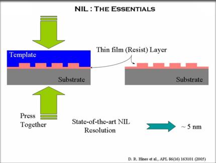
CURRENT STATUS OF NANOIMPRINT LITHOGRAPHY DEVELOPMENT IN CNMM
 U.S. -KOREA Forums on Nanotechnology 1 CURRENT STATUS OF NANOIMPRINT LITHOGRAPHY DEVELOPMENT IN CNMM February 17 th 2005 Eung-Sug Lee,Jun-Ho Jeong Korea Institute of Machinery & Materials U.S. -KOREA Forums
Structuring and bonding of glass-wafers. Dr. Anke Sanz-Velasco
 Structuring and bonding of glass-wafers Dr. Anke Sanz-Velasco Outline IMT Why glass? Components for life science Good bond requirements and evaluation Wafer bonding 1. Fusion bonding 2. UV-adhesive bonding
EE C245 ME C218 Introduction to MEMS Design Fall 2007
 EE C245 ME C218 Introduction to MEMS Design Fall 2007 Prof. Clark T.-C. Nguyen Dept. of Electrical Engineering & Computer Sciences University of California at Berkeley Berkeley, CA 94720 Lecture 11: Bulk
Introduction to Photolithography
 http://www.ichaus.de/news/72 Introduction to Photolithography Photolithography The following slides present an outline of the process by which integrated circuits are made, of which photolithography is
Lecture 11. Etching Techniques Reading: Chapter 11. ECE Dr. Alan Doolittle
 Lecture 11 Etching Techniques Reading: Chapter 11 Etching Techniques Characterized by: 1.) Etch rate (A/minute) 2.) Selectivity: S=etch rate material 1 / etch rate material 2 is said to have a selectivity
Regents of the University of California
 Deep Reactive-Ion Etching (DRIE) DRIE Issues: Etch Rate Variance The Bosch process: Inductively-coupled plasma Etch Rate: 1.5-4 μm/min Two main cycles in the etch: Etch cycle (5-15 s): SF 6 (SF x+ ) etches
EE C245 ME C218 Introduction to MEMS Design Fall 2010
 Lecture Outline EE C245 ME C28 Introduction to MEMS Design Fall 200 Prof. Clark T.-C. Nguyen Dept. of Electrical Engineering & Computer Sciences University of California at Berkeley Berkeley, CA 94720
Figure 1: Graphene release, transfer and stacking processes. The graphene stacking began with CVD
 Supplementary figure 1 Graphene Growth and Transfer Graphene PMMA FeCl 3 DI water Copper foil CVD growth Back side etch PMMA coating Copper etch in 0.25M FeCl 3 DI water rinse 1 st transfer DI water 1:10
Lecture 0: Introduction
 Lecture 0: Introduction Introduction q Integrated circuits: many transistors on one chip q Very Large Scale Integration (VLSI): bucketloads! q Complementary Metal Oxide Semiconductor Fast, cheap, low power
Photolithography Overview 9/29/03 Brainerd/photoclass/ECE580/Overvie w/overview
 http://www.intel.com/research/silicon/mooreslaw.htm 1 Moore s law only holds due to photolithography advancements in reducing linewidths 2 All processing to create electric components and circuits rely
UNIVERSITY OF CALIFORNIA College of Engineering Department of Electrical Engineering and Computer Sciences. Professor Ali Javey. Fall 2009.
 UNIVERSITY OF CALIFORNIA College of Engineering Department of Electrical Engineering and Computer Sciences EE143 Professor Ali Javey Fall 2009 Exam 1 Name: SID: Closed book. One sheet of notes is allowed.
Optical Proximity Correction
 Optical Proximity Correction Mask Wafer *Auxiliary features added on mask 1 Overlay Errors + + alignment mask wafer + + photomask plate Alignment marks from previous masking level 2 (1) Thermal run-in/run-out
EE-612: Lecture 22: CMOS Process Steps
 EE-612: Lecture 22: CMOS Process Steps Mark Lundstrom Electrical and Computer Engineering Purdue University West Lafayette, IN USA Fall 2006 NCN www.nanohub.org Lundstrom EE-612 F06 1 outline 1) Unit Process
Etching. Etching Terminology. Etching Considerations for ICs. Wet Etching. Reactive Ion Etching (plasma etching) Professor N Cheung, U.C.
 Professor N Cheung, U.C.") Etching Etching Terminology Etching Considerations or ICs Wet Etching Reactie Ion Etching (plasma etching) 1 Etch Process - Figures o Merit Etch rate Etch rate uniormity Selectiity Anisotropy 2 (1) Bias
Etching Etching Terminology Etching Considerations or ICs Wet Etching Reactie Ion Etching (plasma etching) 1 Etch Process - Figures o Merit Etch rate Etch rate uniormity Selectiity Anisotropy 2 (1) Bias
Lecture 6 Plasmas. Chapters 10 &16 Wolf and Tauber. ECE611 / CHE611 Electronic Materials Processing Fall John Labram 1/68
 Lecture 6 Plasmas Chapters 10 &16 Wolf and Tauber 1/68 Announcements Homework: Homework will be returned to you on Thursday (12 th October). Solutions will be also posted online on Thursday (12 th October)
Photolithography 光刻 Part II: Photoresists
 微纳光电子材料与器件工艺原理 Photolithography 光刻 Part II: Photoresists Xing Sheng 盛兴 Department of Electronic Engineering Tsinghua University xingsheng@tsinghua.edu.cn 1 Photolithography 光刻胶 负胶 正胶 4 Photolithography
EE C245 ME C218 Introduction to MEMS Design
 EE C245 ME C218 Introduction to MEMS Design Fall 2008 Prof. Clark T.-C. Nguyen Dept. of Electrical Engineering & Computer Sciences University of California at Berkeley Berkeley, CA 94720 Lecture 6: Process
MEEN Nanoscale Issues in Manufacturing. Lithography Lecture 1: The Lithographic Process
 MEEN 489-500 Nanoscale Issues in Manufacturing Lithography Lecture 1: The Lithographic Process 1 Discuss Reading Assignment 1 1 Introducing Nano 2 2 Size Matters 3 3 Interlude One-The Fundamental Science
Dry Etching Zheng Yang ERF 3017, MW 5:15-6:00 pm
 Dry Etching Zheng Yang ERF 3017, email: yangzhen@uic.edu, MW 5:15-6:00 pm Page 1 Page 2 Dry Etching Why dry etching? - WE is limited to pattern sizes above 3mm - WE is isotropic causing underetching -
Techniken der Oberflächenphysik (Techniques of Surface Physics)
") Techniken der Oberflächenphysik (Techniques of Surface Physics) Prof. Yong Lei & Dr. Yang Xu (& Liying Liang) Fachgebiet 3D-Nanostrukturierung, Institut für Physik Contact: yong.lei@tu-ilmenau.de; yang.xu@tu-ilmenau.de;
Techniken der Oberflächenphysik (Techniques of Surface Physics) Prof. Yong Lei & Dr. Yang Xu (& Liying Liang) Fachgebiet 3D-Nanostrukturierung, Institut für Physik Contact: yong.lei@tu-ilmenau.de; yang.xu@tu-ilmenau.de;
Etching Capabilities at Harvard CNS. March 2008
 Etching Capabilities at Harvard CNS March 2008 CNS: A shared use facility for the Harvard Community and New England CNS Provides technical support, equipment and staff. Explicitly multi-disciplinary w/
MICRO AND NANOPROCESSING TECHNOLOGIES
 LECTURE 5 MICRO AND NANOPROCESSING TECHNOLOGIES Introduction Ion lithography X-ray lithography Soft lithography E-beam lithography Concepts and processes Lithography systems Masks and resists Chapt.9.
CVD: General considerations.
 CVD: General considerations. PVD: Move material from bulk to thin film form. Limited primarily to metals or simple materials. Limited by thermal stability/vapor pressure considerations. Typically requires
Clean-Room microfabrication techniques. Francesco Rizzi Italian Institute of Technology
 Clean-Room microfabrication techniques Francesco Rizzi Italian Institute of Technology Miniaturization The first transistor Miniaturization The first transistor Miniaturization The first transistor Miniaturization
Three Approaches for Nanopatterning
 Three Approaches for Nanopatterning Lithography allows the design of arbitrary pattern geometry but maybe high cost and low throughput Self-Assembly offers high throughput and low cost but limited selections
Chapter 9, Etch. Hong Xiao, Ph. D. www2.austin.cc.tx.us/hongxiao/book.htm
 Chapter 9, Etch Hong Xiao, Ph. D. hxiao89@hotmail.com www2.austin.cc.tx.us/hongxiao/book.htm Hong Xiao, Ph. D. www2.austin.cc.tx.us/hongxiao/book.htm 1 Objectives Upon finishing this course, you should
Nanostructures Fabrication Methods
 Nanostructures Fabrication Methods bottom-up methods ( atom by atom ) In the bottom-up approach, atoms, molecules and even nanoparticles themselves can be used as the building blocks for the creation of
DEPOSITION OF THIN TiO 2 FILMS BY DC MAGNETRON SPUTTERING METHOD
 Chapter 4 DEPOSITION OF THIN TiO 2 FILMS BY DC MAGNETRON SPUTTERING METHOD 4.1 INTRODUCTION Sputter deposition process is another old technique being used in modern semiconductor industries. Sputtering
Supplementary Figure 1 Detailed illustration on the fabrication process of templatestripped
 Supplementary Figure 1 Detailed illustration on the fabrication process of templatestripped gold substrate. (a) Spin coating of hydrogen silsesquioxane (HSQ) resist onto the silicon substrate with a thickness
Nano fabrication by e-beam lithographie
 Introduction to nanooptics, Summer Term 2012, Abbe School of Photonics, FSU Jena, Prof. Thomas Pertsch Nano fabrication by e-beam lithographie Lecture 14 1 Electron Beam Lithography - EBL Introduction
Carrier Transport by Diffusion
 Carrier Transport by Diffusion Holes diffuse ÒdownÓ the concentration gradient and carry a positive charge --> hole diffusion current has the opposite sign to the gradient in hole concentration dp/dx p(x)
Supplementary Information Our InGaN/GaN multiple quantum wells (MQWs) based one-dimensional (1D) grating structures
 based one-dimensional (1D) grating structures") Polarized white light from hybrid organic/iii-nitrides grating structures M. Athanasiou, R. M. Smith, S. Ghataora and T. Wang* Department of Electronic and Electrical Engineering, University of Sheffield,
Polarized white light from hybrid organic/iii-nitrides grating structures M. Athanasiou, R. M. Smith, S. Ghataora and T. Wang* Department of Electronic and Electrical Engineering, University of Sheffield,
Photolithography II ( Part 1 )
") 1 Photolithography II ( Part 1 ) Chapter 14 : Semiconductor Manufacturing Technology by M. Quirk & J. Serda Bjørn-Ove Fimland, Department of Electronics and Telecommunication, Norwegian University of Science
1 Photolithography II ( Part 1 ) Chapter 14 : Semiconductor Manufacturing Technology by M. Quirk & J. Serda Bjørn-Ove Fimland, Department of Electronics and Telecommunication, Norwegian University of Science
EE115C Winter 2017 Digital Electronic Circuits. Lecture 3: MOS RC Model, CMOS Manufacturing
 EE115C Winter 2017 Digital Electronic Circuits Lecture 3: MOS RC Model, CMOS Manufacturing Agenda MOS Transistor: RC Model (pp. 104-113) S R on D CMOS Manufacturing Process (pp. 36-46) S S C GS G G C GD
MSN551 LITHOGRAPHY II
 MSN551 Introduction to Micro and Nano Fabrication LITHOGRAPHY II E-Beam, Focused Ion Beam and Soft Lithography Why need electron beam lithography? Smaller features are required By electronics industry:
Top down and bottom up fabrication
 Lecture 24 Top down and bottom up fabrication Lithography ( lithos stone / graphein to write) City of words lithograph h (Vito Acconci, 1999) 1930 s lithography press Photolithography d 2( NA) NA=numerical
The Stanford Nanofabrication Facility. Etch Area Overview. May 21, 2013
 The Stanford Nanofabrication Facility Etch Area Overview May 21, 2013 High Density Plasma Systems Etcher Materials Etched Gases available Wafer Size Applied Materials P5000 MRIE ChA Applied Materials P5000
EE C247B / ME C218 INTRODUCTION TO MEMS DESIGN SPRING 2016 C. NGUYEN PROBLEM SET #4
 Issued: Wednesday, March 4, 2016 PROBLEM SET #4 Due: Monday, March 14, 2016, 8:00 a.m. in the EE C247B homework box near 125 Cory. 1. This problem considers bending of a simple cantilever and several methods
A Novel Approach to the Layer Number-Controlled and Grain Size- Controlled Growth of High Quality Graphene for Nanoelectronics
 Supporting Information A Novel Approach to the Layer Number-Controlled and Grain Size- Controlled Growth of High Quality Graphene for Nanoelectronics Tej B. Limbu 1,2, Jean C. Hernández 3, Frank Mendoza
課程名稱 : 微製造技術 Microfabrication Technology. 授課教師 : 王東安 Lecture 6 Etching
 課程名稱 : 微製造技術 Microfabrication Technology 授課教師 : 王東安 Lecture 6 Etching 1 Lecture Outline Reading Campbell: Chapter 11 Today s lecture Wet etching Chemical mechanical polishing Plasma etching Ion milling
UNIVERSITY OF CALIFORNIA College of Engineering Department of Electrical Engineering and Computer Sciences. Professor Ali Javey. Spring 2009.
 UNIVERSITY OF CALIFORNIA College of Engineering Department of Electrical Engineering and Computer Sciences EE143 Professor Ali Javey Spring 2009 Exam 1 Name: SID: Closed book. One sheet of notes is allowed.
EE 434 Lecture 7. Process Technology
 EE 434 Lecture 7 Process Technology Quiz 4 How many wafers can be obtained from a 2m pull? Neglect the material wasted in the kerf used to separate the wafers. 2m And the number is. 1 8 3 5 6 4 9 7 2 1
Introduction. Photoresist : Type: Structure:
 Photoresist SEM images of the morphologies of meso structures and nanopatterns on (a) a positively nanopatterned silicon mold, and (b) a negatively nanopatterned silicon mold. Introduction Photoresist
Hybrid Wafer Level Bonding for 3D IC
 Hybrid Wafer Level Bonding for 3D IC An Equipment Perspective Markus Wimplinger, Corporate Technology Development & IP Director History & Roadmap - BSI CIS Devices???? 2013 2 nd Generation 3D BSI CIS with
CHARACTERIZATION OF DEEP REACTIVE ION ETCHING (DRIE) PROCESS FOR ELECTRICAL THROUGH-WAFER INTERCONNECTS FOR PIEZORESISTIVE INERTIAL SENSORS
 PROCESS FOR ELECTRICAL THROUGH-WAFER INTERCONNECTS FOR PIEZORESISTIVE INERTIAL SENSORS") CHARACTERIZATION OF DEEP REACTIVE ION ETCHING (DRIE) PROCESS FOR ELECTRICAL THROUGH-WAFER INTERCONNECTS FOR PIEZORESISTIVE INERTIAL SENSORS Maria Suggs, Physics Major, Southern Polytechnic State University
CHARACTERIZATION OF DEEP REACTIVE ION ETCHING (DRIE) PROCESS FOR ELECTRICAL THROUGH-WAFER INTERCONNECTS FOR PIEZORESISTIVE INERTIAL SENSORS Maria Suggs, Physics Major, Southern Polytechnic State University
EECS C245 ME C218 Midterm Exam
 University of California at Berkeley College of Engineering EECS C245 ME C218 Midterm Eam Fall 2003 Prof. Roger T. Howe October 15, 2003 Dr. Thara Srinivasan Guidelines Your name: SOLUTIONS Circle your
Kavli Workshop for Journalists. June 13th, CNF Cleanroom Activities
 Kavli Workshop for Journalists June 13th, 2007 CNF Cleanroom Activities Seeing nm-sized Objects with an SEM Lab experience: Scanning Electron Microscopy Equipment: Zeiss Supra 55VP Scanning electron microscopes
Fiducial Marks for EUV mask blanks. Jan-Peter Urbach, James Folta, Cindy Larson, P.A. Kearney, and Thomas White
 Fiducial Marks for EUV mask blanks Jan-Peter Urbach, James Folta, Cindy Larson, P.A. Kearney, and Thomas White Fiducial marks are laser scribed on 200 mm wafers to enable defect registration on metrology
Photomasks. Photolithography Evolution 9/11/2004 ECE580- MPE/MASKS/PHOTOMASKS.PPT
 Photolithography Evolution 1 : Evolution 2 Photomasks Substrates: Type : thermal expansion Chrome Pellicles Mask: OPC and PSM Fabrication: E-Beam or Laser 3 Photomask Information Websites: http://www.photronics.com/internet/corpcomm/publications/basics101/basics.
EE C245 ME C218 Introduction to MEMS Design Fall 2007
 EE C245 ME C218 Introduction to MEMS Design Fall 2007 Prof. Clark T.-C. Nguyen Dept. of Electrical Engineering & Computer Sciences University of California at Berkeley Berkeley, CA 94720 Lecture 5: ALD,
EE141- Spring 2003 Lecture 3. Last Lecture
 - Spring 003 Lecture 3 IC Manufacturing 1 Last Lecture Design Metrics (part 1) Today Design metrics (wrap-up) IC manufacturing 1 Administrivia Discussion sessions start this week. Only one this week (Dejan
EE C245 ME C218 Introduction to MEMS Design Fall 2007
 EE C245 ME C218 Introduction to MEMS Design Fall 2007 Prof. Clark T.-C. Nguyen Dept. of Electrical Engineering & Computer Sciences University of California at Berkeley Berkeley, CA 94720 Lecture 4: Film
Diffusion and Ion implantation Reference: Chapter 4 Jaeger or Chapter 3 Ruska N & P Dopants determine the resistivity of material Note N lower
 Diffusion and Ion implantation Reference: Chapter 4 Jaeger or Chapter 3 Ruska N & P Dopants determine the resistivity of material Note N lower resistavity than p: due to higher carrier mobility Near linear
High Optical Density Photomasks For Large Exposure Applications
 High Optical Density Photomasks For Large Exposure Applications Dan Schurz, Warren W. Flack, Makoto Nakamura Ultratech Stepper, Inc. San Jose, CA 95134 Microlithography applications such as advanced packaging,
Passionately Innovating With Customers To Create A Connected World
 Passionately Innovating With Customers To Create A Connected World Multi Die Integration Can Material Suppliers Meet the Challenge? Nov 14, 2012 Jeff Calvert - R&D Director, Advanced Packaging Technologies
MICROCHIP MANUFACTURING by S. Wolf
 by S. Wolf Chapter 15 ALUMINUM THIN-FILMS and SPUTTER-DEPOSITION 2004 by LATTICE PRESS CHAPTER 15 - CONTENTS Aluminum Thin-Films Sputter-Deposition Process Steps Physics of Sputter-Deposition Magnetron-Sputtering
1. Narrative Overview Questions
 Homework 4 Due Nov. 16, 010 Required Reading: Text and Lecture Slides on Downloadable from Course WEB site: http://courses.washington.edu/overney/nme498.html 1. Narrative Overview Questions Question 1
SUPPLEMENTARY INFORMATION
 In the format provided by the authors and unedited. DOI: 10.1038/NPHOTON.2016.254 Measurement of non-monotonic Casimir forces between silicon nanostructures Supplementary information L. Tang 1, M. Wang
Y. C. Lee. Micro-Scale Engineering I Microelectromechanical Systems (MEMS)
") Micro-Scale Engineering I Microelectromechanical Systems (MEMS) Y. C. Lee Department of Mechanical Engineering University of Colorado Boulder, CO 80309-0427 leeyc@colorado.edu January 15, 2014 1 Contents
Micro-Scale Engineering I Microelectromechanical Systems (MEMS) Y. C. Lee Department of Mechanical Engineering University of Colorado Boulder, CO 80309-0427 leeyc@colorado.edu January 15, 2014 1 Contents
Fast Bonding of Substrates for the Formation of Microfluidic Channels at Room Temperature
 Supplementary Material (ESI) for Lab on a Chip This journal is The Royal Society of Chemistry 2005 Supporting Information Fast Bonding of Substrates for the Formation of Microfluidic Channels at Room Temperature
Lecture 14 Advanced Photolithography
 Lecture 14 Advanced Photolithography Chapter 14 Wolf and Tauber 1/74 Announcements Term Paper: You are expected to produce a 4-5 page term paper on a selected topic (from a list). Term paper contributes
An environment designed for success
 An environment designed for success The nanofab is a centralized, open-access, training, service, and collaboration facility, focused on academic research and industrial applications in micro- and nanoscale
Plasma Deposition (Overview) Lecture 1
 Lecture 1") Plasma Deposition (Overview) Lecture 1 Material Processes Plasma Processing Plasma-assisted Deposition Implantation Surface Modification Development of Plasma-based processing Microelectronics needs (fabrication
Plasma Deposition (Overview) Lecture 1 Material Processes Plasma Processing Plasma-assisted Deposition Implantation Surface Modification Development of Plasma-based processing Microelectronics needs (fabrication
Plasma etching. Bibliography
 Plasma etching Bibliography 1. B. Chapman, Glow discharge processes, (Wiley, New York, 1980). - Classical plasma processing of etching and sputtering 2. D. M. Manos and D. L. Flamm, Plasma etching; An
ELEC 7364 Lecture Notes Summer Etching. by STELLA W. PANG. from The University of Michigan, Ann Arbor, MI, USA
 ELEC 7364 Lecture Notes Summer 2008 Etching by STELLA W. PANG from The University of Michigan, Ann Arbor, MI, USA Visiting Professor at The University of Hong Kong The University of Michigan on Visiting
NNCI ETCH WORKSHOP - STANFORD NNCI PLASMA ETCH OVERVIEW. Usha Raghuram Stanford Nanofabrication Facility Stanford, CA May 24, 2016
 NNCI ETCH WORKSHOP - STANFORD NNCI PLASMA ETCH OVERVIEW Usha Raghuram Stanford Nanofabrication Facility Stanford, CA May 24, 2016 NNCI AT STANFORD Four labs under NNCI Umbrella at Stanford SNSF Stanford
Physics and Material Science of Semiconductor Nanostructures
 Physics and Material Science of Semiconductor Nanostructures PHYS 570P Prof. Oana Malis Email: omalis@purdue.edu Course website: http://www.physics.purdue.edu/academic_programs/courses/phys570p/ Today
How to work in the NL-cleanroom (1) Multi-application lab: Training, support and tools. By Christiaan Bruinink, Meint de Boer and Bert van den Akker
 Multi-application lab: Training, support and tools. By Christiaan Bruinink, Meint de Boer and Bert van den Akker") How to work in the NL-cleanroom (1) Multi-application lab: Training, support and tools By Christiaan Bruinink, Meint de Boer and Bert van den Akker Contents Multi-application cleanroom Objectives Path
How to work in the NL-cleanroom (1) Multi-application lab: Training, support and tools By Christiaan Bruinink, Meint de Boer and Bert van den Akker Contents Multi-application cleanroom Objectives Path
Supporting Information
 Supporting Information Assembly and Densification of Nanowire Arrays via Shrinkage Jaehoon Bang, Jonghyun Choi, Fan Xia, Sun Sang Kwon, Ali Ashraf, Won Il Park, and SungWoo Nam*,, Department of Mechanical
Overview of the main nano-lithography techniques
 Overview of the main nano-lithography techniques Soraya Sangiao sangiao@unizar.es Outline Introduction: Nanotechnology. Nano-lithography techniques: Masked lithography techniques: Photolithography. X-ray
Yield. Economics. Victor Ovchinnikov. Chapters 36, 37
 Yield. Economics Victor Ovchinnikov Chapters 36, 37 Previous material CMOS Released structural layers MEMS Multilayer metallization Aalto Nanofab, 2017 Microfabrication 2 Content Yield definition Yield
Lecture 8. Photoresists and Non-optical Lithography
 Lecture 8 Photoresists and Non-optical Lithography Reading: Chapters 8 and 9 and notes derived from a HIGHLY recommended book by Chris Mack, Fundamental Principles of Optical Lithography. Any serious student
A Novel Self-aligned and Maskless Process for Formation of Highly Uniform Arrays of Nanoholes and Nanopillars
 Nanoscale Res Lett (2008) 3: 127 DOI 10.1007/s11671-008-9124-6 NANO EXPRESS A Novel Self-aligned and Maskless Process for Formation of Highly Uniform Arrays of Nanoholes and Nanopillars Wei Wu Æ Dibyendu
UHF-ECR Plasma Etching System for Dielectric Films of Next-generation Semiconductor Devices
 UHF-ECR Plasma Etching System for Dielectric Films of Next-generation Semiconductor Devices 1 UHF-ECR Plasma Etching System for Dielectric Films of Next-generation Semiconductor Devices Katsuya Watanabe
Development and Characterization of High Frequency Bulk Mode Resonators
 Excerpt from the Proceedings of the COMSOL Conference 008 Hannover Development and Characterization of High Frequency Bulk Mode Resonators Hossein Pakdast 1*, Zachary James Davis 1 1 DTU Nanotech, Technical