Overview of the main nano-lithography techniques
|
|
|
- Janel Atkins
- 6 years ago
- Views:
Transcription

1 Overview of the main nano-lithography techniques Soraya Sangiao
2 Outline Introduction: Nanotechnology. Nano-lithography techniques: Masked lithography techniques: Photolithography. X-ray lithography. Nanoimprint lithography. Maskless lithography techniques: Electron beam lithography. Ion beam lithography. Scanning probed based lithographies. Summary.

3 Introduction: Nanotechnology What is Nanotechnology? The study of the controlling of matter on an atomic and molecular scale. Generally nanotechnology deals with structures sized between 1 to 100 nanometer in at least one dimension. Nanotechnology involves developing or modifying materials or devices within that size. With 15,342 atoms, this gear is one of the largest nanomechanical devices ever modeled in atomic detail.
4 Introduction: Nanotechnology Some key dates in Nanotechnology: : Michael Faraday discovered ruby gold colloid.
5 Introduction: Nanotechnology Some key dates in Nanotechnology: : Erwin Müller invented the field emission microscope.

6 Introduction: Nanotechnology Some key dates in Nanotechnology: : Bardeen, Shockley and Brattain discovered the semiconductor transistor.
7 Introduction: Nanotechnology Some key dates in Nanotechnology: : Erwin Müller pioneered the field ion microscope.
8 Introduction: Nanotechnology Some key dates in Nanotechnology: : Jack Kilby built the first integrated circuit.
9 Introduction: Nanotechnology Some key dates in Nanotechnology: : Richard Feynman gave the first lecture on technology and engineering at the atomic scale.

10 Introduction: Nanotechnology Some key dates in Nanotechnology: : Gordon Moore described a trend in electronics known as Moore s law.
11 Introduction: Nanotechnology Some key dates in Nanotechnology: : Norio Taniguchi coined the term Nanotechnology.
12 Introduction: Nanotechnology Some key dates in Nanotechnology: : Binnig and Rohrer invented the scanning tunneling microscope.
.")
13 Introduction: Nanotechnology Some key dates in Nanotechnology: : Discovery of the Buckminsterfullerene (C 60 or buckyball).

14 Introduction: Nanotechnology Some key dates in Nanotechnology: : Binnig, Quate and Gerber invented the atomic force microscope.
15 Introduction: Nanotechnology Some key dates in Nanotechnology: Eigler and Schweizer demonstrated the atomic manipulation.


16 Introduction: Nanotechnology Some key dates in Nanotechnology: s 1990s: Consumer products making use of nanotechnology!
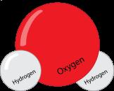

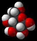

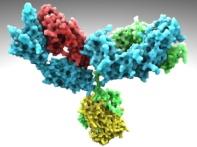
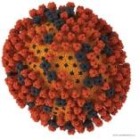
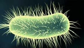
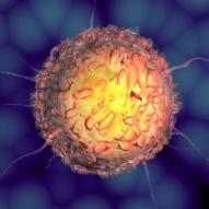

17 Introduction: Nanotechnology How small is Nano? Water Glucose Antibody Virus Bacteria Cancer cell A period Tennis ball Size (nm) Nanodevices

18 Nanolithography techniques Nanolithography: Branch of nanotechnology concerned with the study and application of fabricating nanoscale structures, i.e. patterns with at least one dimension between 1 and 100 nm. Why do we need Nanolithography? We want to do nanopatterning and fabricated useful devices with nanometric dimensions. Even though nature provides a few nanometric systems, in general we need to create them artificially.
.")
19 Nanolithography techniques Approaches to control matter at the nanoscale Top-down approach Thin film deposition techniques + Lithography J. V. Barth et al., Nature 437, 671 (2005). Bottom-up approach Self assembly, self organization
20 Nanolithography techniques Resolution for micro- and nano- fabrication: 10-4 m 10-5 m Micrometric range ( m) 10-6 m 10-7 m 10-8 m Nanometric range ( m) Optical lithography Electron-beam lithography (EBL) Ion-beam lithography (IBL) Nanoimprinting (NIL) Scanning Probe Lithography (SPL-AFM)

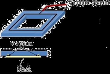
21 Nanolithography techniques Possible classification of nanolithography techniques: Masked lithography techniques: Photolithography. X-ray lithography. Nanoimprint lithography. UV light Mask Resist Sample Substrate Mould Maskless lithography techniques: Electron beam lithography. Ion beam lithography. Scanning probed based lithographies. Resist Sample Electron beam Resist Sample Substrate
22 Photolithography Schematically: 1) Exposure The resist becomes sensitized UV light Mask Resist Sample Substrate 2) Development Immersion in developer fluid. 4) Resist removal 3) Etching Dry or wet etching. Typically acetone Courtesy of J. M. De Teresa, ICMA-Unizar Result: Sample with the same pattern of the mask
23 Photolithography Going over that a little more slowly: - Photolithography masks: UV light Cr alignment crosses (for subsequent steps) Cr motifs (stopper of UV light) Courtesy of J. M. De Teresa, ICMA-Unizar Quartz support (transparent to UV light)
 5 by 5 in area 0.25 in thickness Courtesy of J. M.")
24 Photolithography - Photolithography masks: Cr motifs (stopper of UV light) Quartz support (transparent to UV light) 5 by 5 in area 0.25 in thickness Courtesy of J. M. De Teresa, ICMA-Unizar

")
 Courtesy of J. M.")
25 Photolithography - Photolithography masks: Cr motifs (stopper of UV light) Cr alignment crosses (for subsequent steps) Final sample: (Optical microscope image ) Courtesy of J. M. De Teresa, ICMA-Unizar 4 µm
26 Photolithography - Resists (Photoresists): Viscous fluid formed by a polymer, a photosensitive component and a solvent. Polymer: It provides the properties of viscosity, adherence and resiliance to chemical etching. Solvent: It permits to keep the polymer in solution, allowing its application on the sample. Its concentration changes the viscosity/final thickness. Photosensitive complex: It provides the sensitivity to the UV radiation. This molecule is able to change the solubility of the polymer in the developer.

27 Photolithography - Two types of photoresists: Negative photoresist - Exposure to UV light causes it to polymerize and thus be more difficult to dissolve. Positive photoresist - Exposure to UV light makes it more soluble in the developer. - Developer removes unexposed resist. - Exposed resist is washed away by developer so that the unexposed sample remains. - It results in a pattern supplementary to that of the mask. - It results in an exact copy of the original design.


28 Photolithography - Two types of photoresists: Negative photoresist + Mask #1 Positive photoresist + Mask #2 (supplementary to mask #1) Courtesy of J. M. De Teresa, ICMA-Unizar
29 Photolithography - Spin coating Spin speed: usually in the range rpm Final resist thickness: t 2 η s η = viscosity. s = spin speed.


30 Photolithography - Real equipment for spin coating: -Soft-bake step: Heating at T around 100ºC to eliminate the solvent.
31 Photolithography - Mask aligner: (Exposure system).
32 Photolithography - Exposure modes: Contact: Proximity: Projection: Mask in contact with the photoresist film (gap ~ 0 µm) Gap ~ 10 µm between mask and photoresist. Imaging optics in between the mask and the wafer
 Resolution: 2 bb mmmmmm = 3")

33 Photolithography - Exposure modes: Resolution Contact: Proximity: Projection: Depth of focus: σ=kλ/(na 2 ) Resolution: 2 bb mmmmmm = 3 λλλλ/2 2 bb mmmmmm = 3 λλλλ bb mmmmmm = kkλλ/(nnnn) Example: d=1 µm, λ=365 nm b min 640 nm s =10 µm, λ=365 nm b min 2866 nm k=0.45, λ=248 nm, NA=0.7 b min 160 nm
: -Xe arc lamps: Near continuuos spectrum in the visible 200-750 nm")

34 Photolithography - Mask aligner: Exposure source. Exposure sources (UV): -Xe arc lamps: Near continuuos spectrum in the visible nm with Xe lines above 800 nm. -Hg arc lamps: High energy output in the UV with intense lines between nm. -Hg-Xe arc lamps: Combination of the spectra from Hg and Xe (Xe gas improves start-up and extends operating life).
35 Photolithography - Mask aligner: Exposure source. Exposure sources (DUV): By 1996, transition from an I- line Hg arc lamp to deep-uv excimer laser KrF (248 nm). The physics of excimer laser allows scaling to higher powers, narrower spectral widths and shorter wavelengths.
36 Photolithography - Etching process: Wet etching: By means of reactive liquids Resist Sample Substrate Dry etching: By means of physical etching (sputtering/ionic bombardement) or chemical etching (plasma / RIE). Comparison: Property Wet Dry Anisotropy - + Resolution - + Homogeneity - + Reproducibility - + Profile - + Risk of burns - + Isotropic etching profile Courtesy of J. M. De Teresa, ICMA-Unizar Anisotropic etching profile Cost + -
37 Photolithography - Lift-off process: (positive resist). 1) Exposure UV light Mask Resist Substrate 2) Development 4) Resist removal 3) Sample growth Sample Courtesy of J. M. De Teresa, ICMA-Unizar Result: Sample with pattern supplementary to that of the maks, without etching!
38 Photolithography - Lift-off process: Real example. Mask: + Positive resist. After growing the sample and removing the resist: Courtesy of J. M. De Teresa, ICMA-Unizar
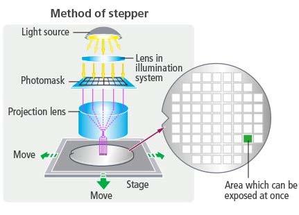
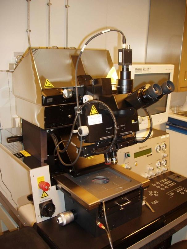
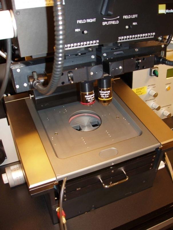
39 Photolithography - Photolithography in IC industry: Stepper.
40 X-ray lithography - X-rays: - Shorter wavelength than UV light Little diffraction effects. - Fine features with vertical sidewalls. - Very large depth of focus Non-flat wafer is OK. - No optics needed: Just an x-ray source, an x-ray resist and an x-ray mask.

41 X-ray lithography - X-ray source: Requirements: Strong, stable, collimated, single frequency Synchrotron radiation: Electromagnetic radiation emitted when charge particles are radially accelerated. High cost!! But - Extremely high intensity. - Tunable. - Very low divergence.

42 X-ray lithography X-ray mask: - Mask substrate: Low atomic number thin membrane. - Absorber: High attenuation, stability under radiation, low microstructural defect density: Au, W, Ta, alloys.
43 X-ray lithography - X-ray resist: - Absorption of x-ray does not produce resist modification. - Photelectrons and Auger electrons are responsible for resist modification. - Any resist for electron beam lithography (PMMA) can be used. Exposure to x-ray (that generates Auger electrons ) cut the PMMA chains, leading to smaller molecular weight that dissolves faster in developers.
44 X-ray lithography - Basic process: Ideal to pattern high resolution and high aspect ratio nanostructures! Development


,")
45 X-ray lithography - Examples: 50 nm lines R. Waser (ed.), Nanoelectronics and Information Technology

46 Nanoimprint lithography - Basic process: - Much simpler in comparison to alternatives! - High throughput. - Low cost for a next-generation technology. Mechanical deformation of the imprint resist. High resolution + high throughput + low cost!! L. Jay Guo, Adv. Mater. 19, 495 (2007).
.")

47 Nanoimprint lithography - Improved process: Step-and-flash imprint lithography (SFIL). L. Jay Guo, Adv. Mater. 19, 495 (2007). Candidate technology for future IC production.


48 Nanoimprint lithography - NIL molds: Fabrication: Material requirements: - Sufficient Young s modulus. - High strength and durability. SEM micrograph: L. Jay Guo, Adv. Mater. 19, 495 (2007).
.")
49 Nanoimprint lithography - NIL resits: Material requirements: - Young s modulus lower than that of the mold. - Sufficiently low viscosity. T > T g Resist cured by UV light. - Good mold-releasing properties. L. Jay Guo, Adv. Mater. 19, 495 (2007). - Good plasma-etching resistance.

50 Nanoimprint lithography - Large area Roll-to-Roll and Roll-to-Plate NIL: High-Throughput application of continuous NIL S. Hyun Ahn and L. Jay Guo, ACS Nano 3, 2304 (2009).


51 Nanoimprint lithography - Large area Roll-to-Roll and Roll-to-Plate NIL: High-Throughput application of continuous NIL 300 nm linewidth, 600 nm height with greatly enhanced throughput. S. Hyun Ahn and L. Jay Guo, ACS Nano 3, 2304 (2009).
 - Sub-100 nm resolution. I. Utke et al., Int. J. Vac. Sci. Technol. B 26, 1197 (2008).")
52 Ion beam lithography - Ion beams: Interaction with matter Focused ion beam (around 30 kev): - Slow heavy atoms: Sputtering of atomic and molecular species from the surface. Focused ion beam lithography: - Direct writing lithography! (No mask) - Sub-100 nm resolution. I. Utke et al., Int. J. Vac. Sci. Technol. B 26, 1197 (2008).
53 Ion beam lithography - Focused Ion Beams sources: High brightness Cryogenic temperature. Less brighter but robust. FIB profile: (spatial distribution) 30 kev Ga+ 1 pa I. Utke et al., Int. J. Vac. Sci. Technol. B 26, 1197 (2008).

. X. Wang et al., Chem.")
54 Ion beam lithography - FIB processes: Nanorotor produced by FIB. A. Santos et al., Nanotechnol. 26, (2015). X. Wang et al., Chem. Mater. 25, 2819 (2013).
55 Summary A. Pimpin et al., Enginner. J. 16, 37 (2011).
56 Thank you for your attention!
Nanostructures Fabrication Methods
 Nanostructures Fabrication Methods bottom-up methods ( atom by atom ) In the bottom-up approach, atoms, molecules and even nanoparticles themselves can be used as the building blocks for the creation of
Nanotechnology Fabrication Methods.
 Nanotechnology Fabrication Methods. 10 / 05 / 2016 1 Summary: 1.Introduction to Nanotechnology:...3 2.Nanotechnology Fabrication Methods:...5 2.1.Top-down Methods:...7 2.2.Bottom-up Methods:...16 3.Conclusions:...19
Techniken der Oberflächenphysik (Techniques of Surface Physics)
") Techniken der Oberflächenphysik (Techniques of Surface Physics) Prof. Yong Lei & Dr. Yang Xu (& Liying Liang) Fachgebiet 3D-Nanostrukturierung, Institut für Physik Contact: yong.lei@tu-ilmenau.de; yang.xu@tu-ilmenau.de;
Techniken der Oberflächenphysik (Techniques of Surface Physics) Prof. Yong Lei & Dr. Yang Xu (& Liying Liang) Fachgebiet 3D-Nanostrukturierung, Institut für Physik Contact: yong.lei@tu-ilmenau.de; yang.xu@tu-ilmenau.de;
MSN551 LITHOGRAPHY II
 MSN551 Introduction to Micro and Nano Fabrication LITHOGRAPHY II E-Beam, Focused Ion Beam and Soft Lithography Why need electron beam lithography? Smaller features are required By electronics industry:
UNIT 3. By: Ajay Kumar Gautam Asst. Prof. Dev Bhoomi Institute of Technology & Engineering, Dehradun
 UNIT 3 By: Ajay Kumar Gautam Asst. Prof. Dev Bhoomi Institute of Technology & Engineering, Dehradun 1 Syllabus Lithography: photolithography and pattern transfer, Optical and non optical lithography, electron,
Lecture 14 Advanced Photolithography
 Lecture 14 Advanced Photolithography Chapter 14 Wolf and Tauber 1/74 Announcements Term Paper: You are expected to produce a 4-5 page term paper on a selected topic (from a list). Term paper contributes
Introduction to Photolithography
 http://www.ichaus.de/news/72 Introduction to Photolithography Photolithography The following slides present an outline of the process by which integrated circuits are made, of which photolithography is
Nanotechnology Nanofabrication of Functional Materials. Marin Alexe Max Planck Institute of Microstructure Physics, Halle - Germany
 Nanotechnology Nanofabrication of Functional Materials Marin Alexe Max Planck Institute of Microstructure Physics, Halle - Germany Contents Part I History and background to nanotechnology Nanoworld Nanoelectronics
Photolithography II ( Part 1 )
") 1 Photolithography II ( Part 1 ) Chapter 14 : Semiconductor Manufacturing Technology by M. Quirk & J. Serda Bjørn-Ove Fimland, Department of Electronics and Telecommunication, Norwegian University of Science
1 Photolithography II ( Part 1 ) Chapter 14 : Semiconductor Manufacturing Technology by M. Quirk & J. Serda Bjørn-Ove Fimland, Department of Electronics and Telecommunication, Norwegian University of Science
MICRO AND NANOPROCESSING TECHNOLOGIES
 LECTURE 5 MICRO AND NANOPROCESSING TECHNOLOGIES Introduction Ion lithography X-ray lithography Soft lithography E-beam lithography Concepts and processes Lithography systems Masks and resists Chapt.9.
CURRENT STATUS OF NANOIMPRINT LITHOGRAPHY DEVELOPMENT IN CNMM
 U.S. -KOREA Forums on Nanotechnology 1 CURRENT STATUS OF NANOIMPRINT LITHOGRAPHY DEVELOPMENT IN CNMM February 17 th 2005 Eung-Sug Lee,Jun-Ho Jeong Korea Institute of Machinery & Materials U.S. -KOREA Forums
Top down and bottom up fabrication
 Lecture 24 Top down and bottom up fabrication Lithography ( lithos stone / graphein to write) City of words lithograph h (Vito Acconci, 1999) 1930 s lithography press Photolithography d 2( NA) NA=numerical
Introduction. Photoresist : Type: Structure:
 Photoresist SEM images of the morphologies of meso structures and nanopatterns on (a) a positively nanopatterned silicon mold, and (b) a negatively nanopatterned silicon mold. Introduction Photoresist
Photolithography 光刻 Part II: Photoresists
 微纳光电子材料与器件工艺原理 Photolithography 光刻 Part II: Photoresists Xing Sheng 盛兴 Department of Electronic Engineering Tsinghua University xingsheng@tsinghua.edu.cn 1 Photolithography 光刻胶 负胶 正胶 4 Photolithography
Kavli Workshop for Journalists. June 13th, CNF Cleanroom Activities
 Kavli Workshop for Journalists June 13th, 2007 CNF Cleanroom Activities Seeing nm-sized Objects with an SEM Lab experience: Scanning Electron Microscopy Equipment: Zeiss Supra 55VP Scanning electron microscopes
Supplementary Figure 1 Detailed illustration on the fabrication process of templatestripped
 Supplementary Figure 1 Detailed illustration on the fabrication process of templatestripped gold substrate. (a) Spin coating of hydrogen silsesquioxane (HSQ) resist onto the silicon substrate with a thickness
Three Approaches for Nanopatterning
 Three Approaches for Nanopatterning Lithography allows the design of arbitrary pattern geometry but maybe high cost and low throughput Self-Assembly offers high throughput and low cost but limited selections
Supplementary Information Our InGaN/GaN multiple quantum wells (MQWs) based one-dimensional (1D) grating structures
 based one-dimensional (1D) grating structures") Polarized white light from hybrid organic/iii-nitrides grating structures M. Athanasiou, R. M. Smith, S. Ghataora and T. Wang* Department of Electronic and Electrical Engineering, University of Sheffield,
Polarized white light from hybrid organic/iii-nitrides grating structures M. Athanasiou, R. M. Smith, S. Ghataora and T. Wang* Department of Electronic and Electrical Engineering, University of Sheffield,
MEEN Nanoscale Issues in Manufacturing. Lithography Lecture 1: The Lithographic Process
 MEEN 489-500 Nanoscale Issues in Manufacturing Lithography Lecture 1: The Lithographic Process 1 Discuss Reading Assignment 1 1 Introducing Nano 2 2 Size Matters 3 3 Interlude One-The Fundamental Science
Nano fabrication by e-beam lithographie
 Introduction to nanooptics, Summer Term 2012, Abbe School of Photonics, FSU Jena, Prof. Thomas Pertsch Nano fabrication by e-beam lithographie Lecture 14 1 Electron Beam Lithography - EBL Introduction
Nanoimprint Lithography
 Nanoimprint Lithography Wei Wu Quantum Science Research Advanced Studies HP Labs, Hewlett-Packard Email: wei.wu@hp.com Outline Background Nanoimprint lithography Thermal based UV-based Applications based
Photolithography Overview 9/29/03 Brainerd/photoclass/ECE580/Overvie w/overview
 http://www.intel.com/research/silicon/mooreslaw.htm 1 Moore s law only holds due to photolithography advancements in reducing linewidths 2 All processing to create electric components and circuits rely
Nanomaterials and their Optical Applications
 Nanomaterials and their Optical Applications Winter Semester 2013 Lecture 02 rachel.grange@uni-jena.de http://www.iap.uni-jena.de/multiphoton Lecture 2: outline 2 Introduction to Nanophotonics Theoretical
Far IR Gas Lasers microns wavelengths, THz frequency Called Terahertz lasers or FIR lasers At this wavelength behaves more like
 Far IR Gas Lasers 10-1500 microns wavelengths, 300 10 THz frequency Called Terahertz lasers or FIR lasers At this wavelength behaves more like microwave signal than light Created by Molecular vibronic
UNIVERSITY OF CALIFORNIA College of Engineering Department of Electrical Engineering and Computer Sciences. Fall Exam 1
 UNIVERSITY OF CALIFORNIA College of Engineering Department of Electrical Engineering and Computer Sciences EECS 143 Fall 2008 Exam 1 Professor Ali Javey Answer Key Name: SID: 1337 Closed book. One sheet
Chapter 3 : ULSI Manufacturing Technology - (c) Photolithography
 Photolithography") Chapter 3 : ULSI Manufacturing Technology - (c) Photolithography 1 Reference 1. Semiconductor Manufacturing Technology : Michael Quirk and Julian Serda (2001) 2. - (2004) 3. Semiconductor Physics and Devices-
Chapter 3 : ULSI Manufacturing Technology - (c) Photolithography 1 Reference 1. Semiconductor Manufacturing Technology : Michael Quirk and Julian Serda (2001) 2. - (2004) 3. Semiconductor Physics and Devices-
ORION NanoFab: An Overview of Applications. White Paper
 ORION NanoFab: An Overview of Applications White Paper ORION NanoFab: An Overview of Applications Author: Dr. Bipin Singh Carl Zeiss NTS, LLC, USA Date: September 2012 Introduction With the advancement
A Novel Self-aligned and Maskless Process for Formation of Highly Uniform Arrays of Nanoholes and Nanopillars
 Nanoscale Res Lett (2008) 3: 127 DOI 10.1007/s11671-008-9124-6 NANO EXPRESS A Novel Self-aligned and Maskless Process for Formation of Highly Uniform Arrays of Nanoholes and Nanopillars Wei Wu Æ Dibyendu
Nano Materials. Nanomaterials
 Nano Materials 1 Contents Introduction Basics Synthesis of Nano Materials Fabrication of Nano Structure Nano Characterization Properties and Applications 2 Fabrication of Nano Structure Lithographic techniques
Clean-Room microfabrication techniques. Francesco Rizzi Italian Institute of Technology
 Clean-Room microfabrication techniques Francesco Rizzi Italian Institute of Technology Miniaturization The first transistor Miniaturization The first transistor Miniaturization The first transistor Miniaturization
There's Plenty of Room at the Bottom
 There's Plenty of Room at the Bottom 12/29/1959 Feynman asked why not put the entire Encyclopedia Britannica (24 volumes) on a pin head (requires atomic scale recording). He proposed to use electron microscope
Technologies VII. Alternative Lithographic PROCEEDINGS OF SPIE. Douglas J. Resnick Christopher Bencher. Sponsored by. Cosponsored by.
 PROCEEDINGS OF SPIE Alternative Lithographic Technologies VII Douglas J. Resnick Christopher Bencher Editors 23-26 February 2015 San Jose, California, United States Sponsored by SPIE Cosponsored by DNS
Optical Proximity Correction
 Optical Proximity Correction Mask Wafer *Auxiliary features added on mask 1 Overlay Errors + + alignment mask wafer + + photomask plate Alignment marks from previous masking level 2 (1) Thermal run-in/run-out
Unconventional Nano-patterning. Peilin Chen
 Unconventional Nano-patterning Peilin Chen Reference Outlines History of patterning Traditional Nano-patterning Unconventional Nano-patterning Ancient Patterning "This is the Elks' land". A greeting at
Broadband transmission grating spectrometer for measuring the emission spectrum of EUV sources
 Broadband transmission grating spectrometer for measuring the emission spectrum of EUV sources Extreme ultraviolet (EUV) light sources and their optimization for emission within a narrow wavelength band
Nanotechnology where size matters
 Nanotechnology where size matters J Emyr Macdonald Overview Ways of seeing very small things What is nanotechnology and why is it important? Building nanostructures What we can do with nanotechnology?
Lecture 8. Photoresists and Non-optical Lithography
 Lecture 8 Photoresists and Non-optical Lithography Reading: Chapters 8 and 9 and notes derived from a HIGHLY recommended book by Chris Mack, Fundamental Principles of Optical Lithography. Any serious student
Far IR (FIR) Gas Lasers microns wavelengths, THz frequency Called Terahertz lasers or FIR lasers At this wavelength behaves more like
 Gas Lasers microns wavelengths, THz frequency Called Terahertz lasers or FIR lasers At this wavelength behaves more like") Far IR (FIR) Gas Lasers 10-1500 microns wavelengths, 300 10 THz frequency Called Terahertz lasers or FIR lasers At this wavelength behaves more like microwave signal than light Created by Molecular vibronic
Far IR (FIR) Gas Lasers 10-1500 microns wavelengths, 300 10 THz frequency Called Terahertz lasers or FIR lasers At this wavelength behaves more like microwave signal than light Created by Molecular vibronic
Enhanced Magnetic Properties of Bit Patterned Magnetic Recording Media by Trench-Filled Nanostructure
 CMRR Report Number 32, Summer 2009 Enhanced Magnetic Properties of Bit Patterned Magnetic Recording Media by Trench-Filled Nanostructure Edward Chulmin Choi, Daehoon Hong, Young Oh, Leon Chen, Sy-Hwang
Self-study problems and questions Processing and Device Technology, FFF110/FYSD13
 Self-study problems and questions Processing and Device Technology, FFF110/FYSD13 Version 2016_01 In addition to the problems discussed at the seminars and at the lectures, you can use this set of problems
Lithography and Etching
 Lithography and Etching Victor Ovchinnikov Chapters 8.1, 8.4, 9, 11 Previous lecture Microdevices Main processes: Thin film deposition Patterning (lithography) Doping Materials: Single crystal (monocrystal)
Carrier Transport by Diffusion
 Carrier Transport by Diffusion Holes diffuse ÒdownÓ the concentration gradient and carry a positive charge --> hole diffusion current has the opposite sign to the gradient in hole concentration dp/dx p(x)
Nanosphere Lithography
 Nanosphere Lithography Derec Ciafre 1, Lingyun Miao 2, and Keita Oka 1 1 Institute of Optics / 2 ECE Dept. University of Rochester Abstract Nanosphere Lithography is quickly emerging as an efficient, low
X-Rays From Laser Plasmas
 X-Rays From Laser Plasmas Generation and Applications I. C. E. TURCU CLRC Rutherford Appleton Laboratory, UK and J. B. DANCE JOHN WILEY & SONS Chichester New York Weinheim Brisbane Singapore Toronto Contents
A Photonic Crystal Laser from Solution Based. Organo-Lead Iodide Perovskite Thin Films
 SUPPORTING INFORMATION A Photonic Crystal Laser from Solution Based Organo-Lead Iodide Perovskite Thin Films Songtao Chen 1, Kwangdong Roh 2, Joonhee Lee 1, Wee Kiang Chong 3,4, Yao Lu 5, Nripan Mathews
Direct write electron beam patterning of DNA complex thin films
 Direct write electron beam patterning of DNA complex thin films R. A. Jones, W. X. Li, H. Spaeth, and A. J. Steckl a Nanoelectronics Laboratory, University of Cincinnati, Cincinnati, Ohio 45221-0030 Received
Fabrication at the nanoscale for nanophotonics
 Fabrication at the nanoscale for nanophotonics Ilya Sychugov, KTH Materials Physics, Kista silicon nanocrystal by electron beam induced deposition lithography Outline of basic nanofabrication methods Devices
PHYS-E0424 Nanophysics Lecture 2: Lithography
 PHYS-E0424 Nanophysics Lecture 2: Lithography 1 Course Overview 19/9 Nanophysics: An introduction 26/9 Nanofabrication: Lithography 3/10 Nanofabrication: Self-organization 10/10 Nanoscale characterization:
Title Single Row Nano-Tribological Printing: A novel additive manufacturing method for nanostructures
 Nano-Tribological Printing: A novel additive manufacturing method for nanostructures H.S. Khare, N.N. Gosvami, I. Lahouij, R.W. Carpick hkhare@seas.upenn.edu carpick@seas.upenn.edu carpick.seas.upenn.edu
Fabrication of Sub-Quarter-Micron Grating Patterns by Employing Lithography
 MCROU,!~'O~C ELSEVER Microelectronic Engineering 46 (1999) 173-177 Fabrication of Sub-Quarter-Micron Grating Patterns by Employing Lithography DUV Holographic L. A. Wang*, C. H. Lin and J. H. Chen nstitute
LECTURE 5 SUMMARY OF KEY IDEAS
 LECTURE 5 SUMMARY OF KEY IDEAS Etching is a processing step following lithography: it transfers a circuit image from the photoresist to materials form which devices are made or to hard masking or sacrificial
Emerging nanopatterning
 Nanotechnology for engineers Winter semester 2006-2007 Emerging nanopatterning Soft-lithography: Microcontact printing Nanoimprint Lithography Stencil lithography Dip-Pen lithography / Nanoscale dispensing
Title of file for HTML: Supplementary Information Description: Supplementary Figures and Supplementary References
 Title of file for HTML: Supplementary Information Description: Supplementary Figures and Supplementary References Supplementary Figure 1. SEM images of perovskite single-crystal patterned thin film with
Nanostructure. Materials Growth Characterization Fabrication. More see Waser, chapter 2
 Nanostructure Materials Growth Characterization Fabrication More see Waser, chapter 2 Materials growth - deposition deposition gas solid Physical Vapor Deposition Chemical Vapor Deposition Physical Vapor
Supplementary Information. Light Manipulation for Organic Optoelectronics Using Bio-inspired Moth's Eye. Nanostructures
 Supplementary Information Light Manipulation for Organic Optoelectronics Using Bio-inspired Moth's Eye Nanostructures Lei Zhou, Qing-Dong Ou, Jing-De Chen, Su Shen, Jian-Xin Tang,* Yan-Qing Li,* and Shuit-Tong
Pattern Transfer- photolithography
 Pattern Transfer- photolithography DUV : EUV : 13 nm 248 (KrF), 193 (ArF), 157 (F 2 )nm H line: 400 nm I line: 365 nm G line: 436 nm Wavelength (nm) High pressure Hg arc lamp emission Ref: Campbell: 7
Nanotechnology. Yung Liou P601 Institute of Physics Academia Sinica
 Nanotechnology Yung Liou P601 yung@phys.sinica.edu.tw Institute of Physics Academia Sinica 1 1st week Definition of Nanotechnology The Interagency Subcommittee on Nanoscale Science, Engineering and Technology
Fabrication of ordered array at a nanoscopic level: context
 Fabrication of ordered array at a nanoscopic level: context Top-down method Bottom-up method Classical lithography techniques Fast processes Size limitations it ti E-beam techniques Small sizes Slow processes
Far IR (FIR) Gas Lasers microns wavelengths, THz frequency Called Terahertz lasers or FIR lasers At this wavelength behaves more like
 Gas Lasers microns wavelengths, THz frequency Called Terahertz lasers or FIR lasers At this wavelength behaves more like") Far IR (FIR) Gas Lasers 10-1500 microns wavelengths, 300 10 THz frequency Called Terahertz lasers or FIR lasers At this wavelength behaves more like microwave signal than light Created by Molecular vibronic
Far IR (FIR) Gas Lasers 10-1500 microns wavelengths, 300 10 THz frequency Called Terahertz lasers or FIR lasers At this wavelength behaves more like microwave signal than light Created by Molecular vibronic
Chapter 10. Nanometrology. Oxford University Press All rights reserved.
 Chapter 10 Nanometrology Oxford University Press 2013. All rights reserved. 1 Introduction Nanometrology is the science of measurement at the nanoscale level. Figure illustrates where nanoscale stands
Introduction to Electron Beam Lithography
 Introduction to Electron Beam Lithography Boštjan Berčič (bostjan.bercic@ijs.si), Jožef Štefan Institute, Jamova 39, 1000 Ljubljana, Slovenia 1. Introduction Electron Beam Lithography is a specialized
ETCHING Chapter 10. Mask. Photoresist
 ETCHING Chapter 10 Mask Light Deposited Substrate Photoresist Etch mask deposition Photoresist application Exposure Development Etching Resist removal Etching of thin films and sometimes the silicon substrate
Advanced Texturing of Si Nanostructures on Low Lifetime Si Wafer
 Advanced Texturing of Si Nanostructures on Low Lifetime Si Wafer SUHAILA SEPEAI, A.W.AZHARI, SALEEM H.ZAIDI, K.SOPIAN Solar Energy Research Institute (SERI), Universiti Kebangsaan Malaysia (UKM), 43600
J. Photopolym. Sci. Technol., Vol. 22, No. 5, Fig. 1. Orthogonal solvents to conventional process media.
 originates from the limited number of options regarding orthogonal solvents, i.e. solvents that do not dissolve or adversely damage a pre-deposited organic materials layer. The simplest strategy to achieve
Presentation Phys Katia GASPERI. Statistical study of single DNA molecules into dynamic array
 Presentation Phys 730 - Katia GASPERI Statistical study of single DNA molecules into dynamic array 1 Statistical study of single DNA molecules into dynamic array - Research project lead by Laurence SALOME
UNIVERSITY OF CALIFORNIA College of Engineering Department of Electrical Engineering and Computer Sciences. Professor Ali Javey. Fall 2009.
 UNIVERSITY OF CALIFORNIA College of Engineering Department of Electrical Engineering and Computer Sciences EE143 Professor Ali Javey Fall 2009 Exam 1 Name: SID: Closed book. One sheet of notes is allowed.
Revealing High Fidelity of Nanomolding Process by Extracting the Information from AFM Image with Systematic Artifacts
 Revealing High Fidelity of Nanomolding Process by Extracting the Information from AFM Image with Systematic Artifacts Sajal Biring* Department of Electronics Engineering and Organic Electronics Research
Presentation Phys Katia GASPERI. Statistical study of single DNA molecules into dynamic array
 Presentation Phys 730 - Katia GASPERI Statistical study of single DNA molecules into dynamic array 1 Statistical study of single DNA molecules into dynamic array - Research project lead by Laurence SALOME
Seminars in Nanosystems - I
 Seminars in Nanosystems - I Winter Semester 2011/2012 Dr. Emanuela Margapoti Emanuela.Margapoti@wsi.tum.de Dr. Gregor Koblmüller Gregor.Koblmueller@wsi.tum.de Seminar Room at ZNN 1 floor Topics of the
Formation mechanism and Coulomb blockade effect in self-assembled gold quantum dots
 Formation mechanism and Coulomb blockade effect in self-assembled gold quantum dots S. F. Hu a) National Nano Device Laboratories, Hsinchu 300, Taiwan R. L. Yeh and R. S. Liu Department of Chemistry, National
Photoresist Profile. Undercut: negative slope, common for negative resist; oxygen diffusion prohibits cross-linking; good for lift-off.
 Photoresist Profile 4-15 Undercut: negative slope, common for negative resist; oxygen diffusion prohibits cross-linking; good for lift-off undercut overcut Overcut: positive slope, common to positive resist,
Sub-5 nm Patterning and Applications by Nanoimprint Lithography and Helium Ion Beam Lithography
 Sub-5 nm Patterning and Applications by Nanoimprint Lithography and Helium Ion Beam Lithography Yuanrui Li 1, Ahmed Abbas 1, Yuhan Yao 1, Yifei Wang 1, Wen-Di Li 2, Chongwu Zhou 1 and Wei Wu 1* 1 Department
Nano-Lithography. Edited by Stefan Landis
 Nano-Lithography Edited by Stefan Landis IST^ m WILEY Table of Contents Foreword Jörge DE SOUSA NORONHA Introduction Michel BRILLOUET xi xvii Chapter 1. X-ray Lithography: Fundamentals and Applications
Supplementary Information
 Supplementary Information Experimental Section Hybrid Nanoparticle Synthesis The hafnium nanoparticles surface-modified with methacrylic acid (MAA, Sigma Aldrich, 99%), trans 2, 3-dimethylacrylic acid
100 nm period gratings produced by lithographically induced self-construction
 INSTITUTE OFPHYSICS PUBLISHING Nanotechnology 14 (2003) 786 790 NANOTECHNOLOGY PII: S0957-4484(03)55891-3 100 nm period gratings produced by lithographically induced self-construction Xinya Lei, Lin Wu,
Table of Contents. Foreword... Jörge DE SOUSA NORONHA. Introduction... Michel BRILLOUËT
 Table of Contents Foreword... Jörge DE SOUSA NORONHA Introduction... Michel BRILLOUËT xi xvii Chapter 1. Photolithography... 1 Philippe BANDELIER, Anne-Laure CHARLEY and Alexandre LAGRANGE 1.1. Introduction...
DQN Positive Photoresist
 UNIVESITY OF CALIFONIA, BEKELEY BEKELEY DAVIS IVINE LOS ANGELES IVESIDE SAN DIEGO SAN FANCISCO SANTA BABAA SANTA CUZ DEPATMENT OF BIOENGINEEING 94720-1762 BioE 121 Midterm #1 Solutions BEKELEY, CALIFONIA
An Optimal Substrate Design for SERS: Dual-Scale Diamond-Shaped Gold Nano-Structures Fabricated via Interference Lithography
 Supporting Information An Optimal Substrate Design for SERS: Dual-Scale Diamond-Shaped Gold Nano-Structures Fabricated via Interference Lithography Hyo-Jin Ahn a, Pradheep Thiyagarajan a, Lin Jia b, Sun-I
Supplementary Figure 1 Dark-field optical images of as prepared PMMA-assisted transferred CVD graphene films on silicon substrates (a) and the one
 and the one") Supplementary Figure 1 Dark-field optical images of as prepared PMMA-assisted transferred CVD graphene films on silicon substrates (a) and the one after PBASE monolayer growth (b). 1 Supplementary Figure
Supplementary Figure 1 Dark-field optical images of as prepared PMMA-assisted transferred CVD graphene films on silicon substrates (a) and the one after PBASE monolayer growth (b). 1 Supplementary Figure
Photonics applications 5: photoresists
 IMI-NFG s Mini Course on Chalcogenide Glasses Lecture 11 Photonics applications 5: photoresists Himanshu Jain Department of Materials Science & Engineering Lehigh University, Bethlehem, PA 18015 H.Jain@Lehigh.edu
IC Fabrication Technology
 IC Fabrication Technology * History: 1958-59: J. Kilby, Texas Instruments and R. Noyce, Fairchild * Key Idea: batch fabrication of electronic circuits n entire circuit, say 10 7 transistors and 5 levels
Etching: Basic Terminology
 Lecture 7 Etching Etching: Basic Terminology Introduction : Etching of thin films and sometimes the silicon substrate are very common process steps. Usually selectivity, and directionality are the first
Micro- and Nano-Technology... for Optics
 Micro- and Nano-Technology...... for Optics U.D. Zeitner Fraunhofer Institut für Angewandte Optik und Feinmechanik Jena Today: 1. Introduction E. Bernhard Kley Institute of Applied Physics Friedrich-Schiller
Nano fabrication and optical characterization of nanostructures
 Introduction to nanooptics, Summer Term 2012, Abbe School of Photonics, FSU Jena, Prof. Thomas Pertsch Nano fabrication and optical characterization of nanostructures Lecture 12 1 Optical characterization
Carbon Nanotube Thin-Films & Nanoparticle Assembly
 Nanodevices using Nanomaterials : Carbon Nanotube Thin-Films & Nanoparticle Assembly Seung-Beck Lee Division of Electronics and Computer Engineering & Department of Nanotechnology, Hanyang University,
The fabrication of periodic metal nanodot arrays through pulsed laser melting induced fragmentation of metal nanogratings
 IOP PUBLISHING Nanotechnology 20 (2009) 285310 (5pp) NANOTECHNOLOGY doi:10.1088/0957-4484/20/28/285310 The fabrication of periodic metal nanodot arrays through pulsed laser melting induced fragmentation
Supplementary Information Effects of asymmetric nanostructures on the extinction. difference properties of actin biomolecules and filaments
 Supplementary Information Effects of asymmetric nanostructures on the extinction difference properties of actin biomolecules and filaments 1 E. H. Khoo, 2 Eunice S. P. Leong, 1 W. K. Phua, 2 S. J. Wu,
GRAPHENE ON THE Si-FACE OF SILICON CARBIDE USER MANUAL
 GRAPHENE ON THE Si-FACE OF SILICON CARBIDE USER MANUAL 1. INTRODUCTION Silicon Carbide (SiC) is a wide band gap semiconductor that exists in different polytypes. The substrate used for the fabrication
Positioning, Structuring and Controlling with Nanoprecision
 Positioning, Structuring and Controlling with Nanoprecision Regine Hedderich 1,2, Tobias Heiler 2,3, Roland Gröger 2,3, Thomas Schimmel 2,3 and Stefan Walheim 2,3 1 Network NanoMat 2 Institute of Nanotechnology,
Woo Jin Hyun, Ethan B. Secor, Mark C. Hersam, C. Daniel Frisbie,* and Lorraine F. Francis*
 Woo Jin Hyun, Ethan B. Secor, Mark C. Hersam, C. Daniel Frisbie,* and Lorraine F. Francis* Dr. W. J. Hyun, Prof. C. D. Frisbie, Prof. L. F. Francis Department of Chemical Engineering and Materials Science
Nanolithography Techniques
 Nanolithography Techniques MSE 505 / MSNT 505 P. Coane Outline What Is Nanotechnology? The Motivation For Going Small Nanofabrication Technologies Basic Techniques Nano Lithography NANOTECHNOLOGY Nanotechnology
Materials. Definitions of nanotechnology. The term nanotechnology was invented by Professor Norio Taniguchi at the University of Tokyo in 1971.
 Materials Definitions of nanotechnology The term nanotechnology was invented by Professor Norio Taniguchi at the University of Tokyo in 1971. The original definition, translated into English Nano-technology'
Supplementary information for
 Supplementary information for Transverse electric field dragging of DNA in a nanochannel Makusu Tsutsui, Yuhui He, Masayuki Furuhashi, Rahong Sakon, Masateru Taniguchi & Tomoji Kawai The Supplementary
Nanostructure Fabrication Using Selective Growth on Nanosize Patterns Drawn by a Scanning Probe Microscope
 Nanostructure Fabrication Using Selective Growth on Nanosize Patterns Drawn by a Scanning Probe Microscope Kentaro Sasaki, Keiji Ueno and Atsushi Koma Department of Chemistry, The University of Tokyo,
Resonator Fabrication for Cavity Enhanced, Tunable Si/Ge Quantum Cascade Detectors
 Resonator Fabrication for Cavity Enhanced, Tunable Si/Ge Quantum Cascade Detectors M. Grydlik 1, P. Rauter 1, T. Fromherz 1, G. Bauer 1, L. Diehl 2, C. Falub 2, G. Dehlinger 2, H. Sigg 2, D. Grützmacher
Ultrafast Nano Imprint Lithography
 Ultrafast Nano Imprint Lithography Imprint in less than 1 sec Logos Anti-counterfeiting nanostructures Miniaturized QRs Customized designs 2 Pulsed-NIL technology enables printing times in less than 100
Figure 1: Graphene release, transfer and stacking processes. The graphene stacking began with CVD
 Supplementary figure 1 Graphene Growth and Transfer Graphene PMMA FeCl 3 DI water Copper foil CVD growth Back side etch PMMA coating Copper etch in 0.25M FeCl 3 DI water rinse 1 st transfer DI water 1:10
Microelectronic Engineering
 Microelectronic Engineering 87 (2010) 899 903 Contents lists available at ScienceDirect Microelectronic Engineering journal homepage: www.elsevier.com/locate/mee A versatile pattern inversion process based
Nanofabrication of direct positioning atomic force microscope (AFM) probes and a novel method to attain controllable lift-off
 probes and a novel method to attain controllable lift-off") Nanofabrication of direct positioning atomic force microscope (AFM) probes and a novel method to attain controllable lift-off by Shuo Zheng A thesis presented to University of Waterloo in the fulfillment
Nanofabrication of direct positioning atomic force microscope (AFM) probes and a novel method to attain controllable lift-off by Shuo Zheng A thesis presented to University of Waterloo in the fulfillment
EE 434 Lecture 7. Process Technology
 EE 434 Lecture 7 Process Technology Quiz 4 How many wafers can be obtained from a 2m pull? Neglect the material wasted in the kerf used to separate the wafers. 2m And the number is. 1 8 3 5 6 4 9 7 2 1